PROCEEDINGS OF SPIE
SPIEDigitalLibrary.org/conference-proceedings-of-spieExperimental demonstration of
sub-wavelength imaging by left-handed
metamaterials
Experimental demonstration of sub-wavelength imaging by left
handed metamaterials
Ekmel Ozbay*
Nanotechnology Research Center, Bilkent University, Bilkent, 06800 Ankara, TURKEY
ABSTRACT
We review the studies conducted in our group concerning electromagnetic properties of metamaterials and photonic crystals with negative effective index of refraction. In particular, we demonstate the true left handed behavior of a 2D composite metamaterial, by analyzing the electric and magnetic response of the material components systematically. The negative refraction, subwavelength focusing, and flat lens phenomena using left handed metamaterials and photonic crystals are also presented.
Keywords: Negative refraction, negative phase velocity, photonic crystal, split ring resonator, left-handed medium, metamaterial
Once put as a theoretical proposition, materials with negative index of refraction[1] are becoming an increasingly intense research subject in recent years, thanks to their experimental realization.[2,3] These composite metamaterials (CMMs) are consisting of two components which have permittivity ε(ω) < 0 and permeability µ(ω) < 0 respectively over a certain frequency range, so that the index of refraction of the effective medium becomes
n
eff=
ε
µ
<
0
. They are also called left-handed materials named by the parity of the coordinate system formed by electric, magnetic and wavevectors of the field. Novel electromagnetic phenomena stemming from the presence of neff<0, such as negativerefraction, and superlensing carry potential for revolutionary applications in optics. On the other hand, another novel research area called photonic crystals (PCs)[10,11] emerged as an alternative platform to investigate certain electromagnetic phenomena based on neff<0, where the band structure of the PC can lead to negative dispersion for
electromagnetic waves, in analogy to negative effective mass of electron in a solid.[4, 5]
In this paper, we review a number of studies based on both approaches to investigate the electromagnetic and optic properties of media with neff < 0. In the first part, we discuss the CMM approach, and focus on the transmission characteristics of CMMs to identify their left-handed behavior accurately. In the second part, experimental and numerical results concerning negative refraction and focusing of EM waves using PCs will be presented. Two basic mechanisms arising from the band structure of PCs are employed to obtain negative refraction. We found that focusing abilities of a PC slab can surpass that of conventional (i.e. positive refractive) materials, providing both subwavelength resolution and true flat lens behavior.
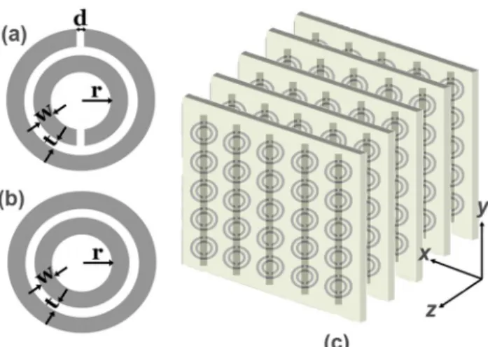
The CMMs (Fig.1 c) consist of the so-called split ring resonators (SRRs) [6] and wires [7] which provide magnetic and electric resonances, respectively. The SRR (Fig. 1.a) and closed-SRR (CSRR) (Fig. 1.b) units are fabricated on circuit boards (type: FR4) with a copper deposited layer of thickness 30 µm by etching. The geometrical and material parameters can be found in another publication.[8] SRR units are arranged periodically with 5, 15, and 18 unit cells in x,
y and z directions, with respective periods of ax = ay = 8.8 mm, and az = 6.5 mm. Experimental setup consists of a HP 8510C network analyzer, and microwave horn antennas. The incident field propagates along the x direction with E, and H, along y and z directions, respectively.
(a)
—
(b)
(C)
Figure 1 :Schematics of (a) a single split ring resonator (SRR) (b) a ring resonator with splits closed (CSRR) (c) Periodic CMM composed of SRRs on one side, wires on the other side of dielectric board.
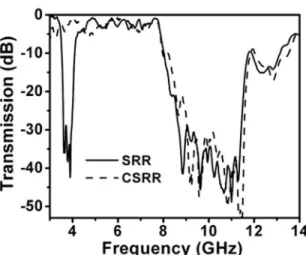
Figure 2 shows the measured transmission spectra of periodic SRRs (solid line) and CSRRs (dashed line) between 3-14 GHz. The first bandgap (3.55-4.05 GHz) of the SRR medium is not present in the CSRR medium, which marks the µ < 0 region. In contrast, the second bandgap (8.1-11.9 GHz) is present for both the SRR and CSRR medium. This measurement clearly distinguishes the µ < 0 gaps from the ε < 0, and from the periodicity induced Bragg gaps of the SRR.
In addition, the SRRs also exhibit an electric response which is similar to that of a periodic cut-wire medium. As a result, when combined with wires in a CMM, the SRRs contribute to the effective permittivity of the CMM, causing a downward shift of the plasma frequency, ωp, determined solely from wire structures.[9] The amount of the shift is crucial, because, if ωp shifts below ωm, i.e. below the µ < 0 gap, this would render the CMM as a right-handed medium. We have designed the present SRRs such that the µ < 0 gap of the SRR medium between 3.55 - 4.05 GHz is not obscured by this shift. The CMM structure is made of Nx = 5, Ny = 15, and Nz = 24 unit cells. The transmission spectra for SRR only (solid line), wire only (dashed line) and CMM (bold solid line) periodic structures are displayed in Fig. 3. The CMM pass band 3.6 – 4.1 GHz, exactly coincides where both ε and µ are negative. The peak transmission at 3.9 GHz is -1.2 dB, which is a significantly high value for a material made of metals. The electric response contribution of SRRs is also evident here: The transmission starting at 5.3 GHz (solid line) marks the ωp of the CMM, which is significantly lower than that of wire-only structure at ~8 GHz (dotted line).
C
0
Cl) Cl) E CI-4
6 8 10 12 14Frequency (GHz)
Frequency (GHz}Figure 2 :Measured transmission spectra of a periodic SRR medium (solid line) and periodic CSRR medium (dashed line) between 3-14 GHz.
Figure 3. Comparison of the transmission spectra of SRR (dashed), wire (dotted) and CMM solid line.Note the shift of plasma cut-off frequency from 8 GHz determined from wires to 5.3 GHz in CMM.
In photonic crystals, the periodic modulation of the dielectric constant leads to a band structure for the propagation of electromagnetic waves.[10, 11] By modifying periodicity and dielectric constant, it is possible to obtain transmission bands with convex equal-frequency contours in k-space, which leads to negative refraction.
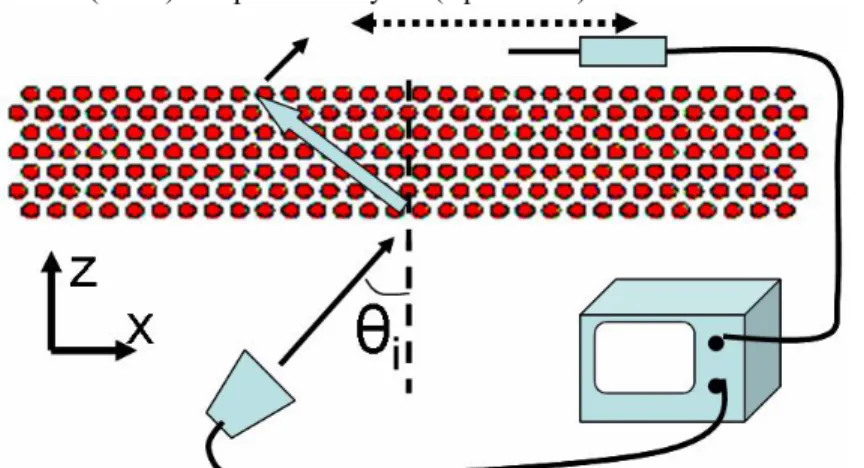
In this section we present the experimental demonstration of the negative refraction phenomenon.[12] The PC consists of a square array of alumina rods in air. The frequency range that gives neff < 0 extends from 0.21 (13.10 GHz) to 0.25 (15.44 GHz) as indicated on the TM band structure shown in Fig. 4. The refraction measurements are performed by horn/monopole antennas as emitter/detector pair and a network analyzer, as shown in Fig. 5. In Fig. 6(a), the lateral beam profiles scanned at the second PC interface by the detector antenna are shown. The center of the outgoing Gaussian beam is shifted towards the left hand side of the center of the incident Gaussian beam, which demonstrates the negative refraction. Using Snell’s Law, we found neff -1.94 experimentally and -2.06 calculated by the
finite-difference-TM band Siruclure X M F I
••s•neeeeeeesseeeseenesseeee
I••sss•ss••••se,sss••e•s•ss
F•essteeeeee••••ee••t'e•s••stess
•eeee...S.e.eeeI.esSn.eee.eees
-1 I/
0
4
Figure 4 [Left] TM polarized band structure of the 2D PC. Shaded frequency band exhibits negative refraction. [Right] Equal-frequency contours of air (circle) and photonic crystal (square-like).
Figure 5 Schematic top view of the refraction experiment setup consisting of emitter (horn antenna), 2D PC (cubic or hexagonal), receiver (monopole antenna) and the network analyzer.
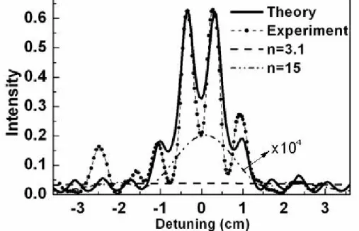
Subwavelength resolution using negative refractive materials has been theoretically suggested.[13] We perform the experiments and simulations with two incoherent point sources 0.7 mm away from the PC, which are separated by a distance of 6.78 mm (~λ/3), and having frequencies 13.698 GHz and 13.608 GHz respectively. Fig. 7 shows the measured and simulated power distribution at 0.7 mm away from the outgoing interface the PC. The peaks corresponding to each point source are clearly resolved. To our knowledge, this is the first experimental observation of subwavelength resolution of two incoherent sources using negative refractive materials.[14] For comparison, the simulations made for a homogeneous slab with n = 3.1 (alumina) and n = 15 (hypothetical material) are also indicated. Evidently, subwavelength resolution is not achieved even with unrealistically large refractive index. Besides, the large reflection due to the high index contrast significantly reduces the transmitted power when compared to 63% transmission obtained from the PC. So, even if the observed subwavelength resolution is a near field effect, this can not be achieved by ubiquitous materials.
(a)
— 1 .00.8
O.6
0
C 0.4 a, C 0.2 0. -6 -4 -2 0 2(b)
positive Refraction.1.0-80.4
' 0.2
0. Detuning (cm)0.2
-3
-2
-1
0
12
3
Detuning (cm)
Figure 6 (a) Negative refraction through the photonic crystal. (b) Same as in (a) but refraction through a crystal of polystryene pellets
ACKNOWLEDGMENTS
This work is supported by TUBITAK, EU-DALHM, EU-METAMORPHOSE, and EU-PHOREMOST. One of the authors (Ekmel Ozbay) acknowledges partial support from Turkish Academy of Sciences.
REFERENCES
[1] V. G. Veselago, Sov. Phys. Usp. 10, 504 (1968).
[2] D. R. Smith, W. J. Padilla, D. C. Vier, S. C. Nemat-Nasser, and S. Schultz, Phys. Rev. Lett, 84, 4184 (2000).
[3] R. A. Shelby, D. R. Smith, and S. Schultz, Science 292, 77 (2001). [4] M. Notomi, Phys. Rev. B 62, 10696 (2000).
[5] C. Luo, S. G. Johnson, J. D. Joannoupoulos, and J. B. Pendry, Phys. Rev. B 65, R201104 (2002). [6] J. B. Pendry, A. J. Holden, W. J. Stewart, and I. Youngs, Phys. Rev. Lett. 76, 4773 (1996).
[7] J. B. Pendry, A. J. Holden, D. J. Robins, and W. J. Stewart, IEEE Transac. Microw. Th. and Techn. 47, 2075 (1999).
[8] K. Aydin, K. Guven, L. Zhang, M. Kafesaki, C. M. Soukoulis, and E. Ozbay, Opt. Lett. 29, 2623 (2004). Koray Aydin, Kaan Guven, C. M. Soukoulis, and Ekmel Ozbay “Observation of negative refraction and negative phase velocity in left-handed metamaterials,” Applied Physics Letters, volume 86, 124102 (2005).
[9] T. Koschny, M. Kafesaki, E. N. Economou, and C. M. Soukoulis, Phys. Rev. Lett. 93, 107402, (2004). [10] J. D. Joannopoulos, R. D. Meade, and J. N. Winn, Photonic Crystals: Molding the Flow of Light,
Princeton University Press, Princeton, (1995).
[11] C. M. Soukoulis (ed.), Photonic Crystals and Light Localization in the 21st Century, Kluwer, Dortrecht, (2000).
[12] E. Cubukcu, K. Aydin, E. Ozbay, S. Foteinopoulou, and C. M. Soukoulis, Nature 423, 604 (2003). [13] J. B. Pendry, Phys. Rev. Lett. 85, 3966 (2000).
[14] E. Cubukcu, K. Aydin, E. Ozbay, S. Foteinopoulou, and C. M. Soukoulis, Phys. Rev. Lett. 91, 207401 (2003).