Donmez, F Sarcan, S B Lisesivdin et al.
IOP PUBLISHING SEMICONDUCTOR SCIENCE AND TECHNOLOGY
Semicond. Sci. Technol. 23 (2008) 095008 (7pp) doi:10.1088/0268-1242/23/9/095008
Growth parameter investigation of
Al0.25Ga0.75N
/GaN/AlN heterostructures
with Hall effect measurements
S B Lisesivdin
1, S Demirezen
1, M D Caliskan
2, A Yildiz
3, M Kasap
1,
S Ozcelik
1and E Ozbay
2,4,51 Department of Physics, Faculty of Science and Arts, Gazi University, Teknikokullar, 06500 Ankara, Turkey 2 Nanotechnology Research Center, Bilkent University, Bilkent, 06800 Ankara, Turkey
3 Department of Physics, Faculty of Science and Arts, Ahi Evran University, 40100 Kirsehir, Turkey 4 Department of Physics, Bilkent University, Bilkent, 06800 Ankara, Turkey
5 Department of Electrical and Electronics Engineering, Bilkent University, Bilkent, 06800 Ankara, Turkey
E-mail: [email protected]
Received 29 January 2008, in final form 6 July 2008 Published 8 August 2008
Online at stacks.iop.org/SST/23/095008
Abstract
Hall effect measurements on unintentionally doped Al0.25Ga0.75N/GaN/AlN heterostructures grown by metal organic chemical vapor deposition (MOCVD) were carried out as a function of temperature (20–300 K) and magnetic field (0–1.4 T). Magnetic-field-dependent Hall data are analyzed using the quantitative mobility spectrum analysis (QMSA) technique. The QMSA technique successfully separated electrons in the 2D electron gas (2DEG) at the Al0.25Ga0.75N/GaN interface from other 2D and 3D conduction mechanisms of the samples. 2DEG mobilities, carrier densities and conductivities of the investigated samples are
compared at room temperature and low temperature (20 K). For a detailed investigation of the 2DEG-related growth parameters, the scattering analyses of the extracted 2DEG were carried out for all of the samples. Using the results of the scattering analyses, the relation between the growth and scattering parameters was investigated. Increments in the interface roughness (IFR) are reported with the increased GaN buffer growth temperatures. In addition, a linear relation between the deformation potential and interface roughness (IFR) scattering is pointed out for the investigated samples, which may lead to a better understanding of the mechanism of IFR scattering.
1. Introduction
The AlGaN/GaN/(AlN) material system was studied extensively over the last few decades because of its optical and electrical properties. High-performance electronic devices and semiconductor power amplifiers with high frequency and power capabilities are in high demand for use in many semiconductor applications. AlxGa1−xN/GaN
heterostructures [1] have been demonstrated for these power applications at high temperatures with a high cutoff frequency and a large sheet carrier density [2–4]. Various studies of the electrical transport properties of these heterostructures have been reported in the literature [5–12]. AlxGa1−xN/GaN
heterostructures show room temperature electron mobilities of ∼1500 cm2 V−1 s−1 with average electron velocities of ∼1.25 × 107 cm s−1 and a very good high-frequency response. The crystal growth process often causes strong intrinsic electric fields that are normal to the plane of the heterostructure [13]. These electric fields are mostly strain induced, and they can be further enhanced by contributions from spontaneous polarization [14]. Because of the large piezoelectric constants of the material system, piezoelectric polarization is very strong in an AlGaN on GaN [15]. Because of the electric fields that are induced by these strong polarization fields, electron-confining potential wells are generated at the related heterojunction. As a result,
0268-1242/08/095008+07$30.00 © 2008 IOP Publishing Ltd Printed in the UK
Table 1. Growth temperatures and thicknesses of the investigated samples.
Sample A Sample B Sample C
Thickness (nm) Temperature (◦C) Thickness (nm) Temperature (◦C) Thickness (nm) Temperature (◦C)
GaN cap 3 1080 3 1080 2 1085 AlGaN barrier 27 1080 27 1080 25 1085 HRa GaN buffer 2143 1075 2143 1075 2000 1075 GaN buffer 320 1035 320 1025 – 1050 AlN buffer 250 1125 250 1125 500 1150 AlN nucleation Sapphire wafer 10 840 10 840 15 840
a High growth rated.
two-dimensional electron gas (2DEG) densities larger than 1013 cm−2 havebeenobservedevenwithunintentionallydoped structures [16–18].
A buffer layer is one of the important factors that determine the quality of the epitaxial layers. Certain improvements can be achieved in structural, electrical and optical properties by changing the growth parameters of the buffer layer. To perform a complete 2DEG channel pinchoff and low loss at high frequencies, the achievement of the semi-insulating buffer is important for these heterostructures [19,
20]. It is well known that the unintentionally doped GaN grown on the sapphire substrate by metal organic chemical vapor deposition (MOCVD) typically shows n-type conductivity due to oxygen impurity diffusion during growth [21]. In addition, heterostructures with a single GaN buffer grown on sapphire have poor crystal qualities because of high dislocation densities, which have negative effects on the surface morphology and interface roughness [22, 23]. It was reported that an AlN buffer layer enhances nucleation and lateral growth [24, 25]. Our previous work [26] showed that an improved SI–GaN layer can be achieved by the growth of a high-temperature (HT) AlN buffer layer on the sapphire substrate. To achieve better 2DEG properties, such as the mobility and carrier density, the composition transition at the AlGaN/GaN interface must be sudden and the interface must besmooth. Itisknownthat[16, 27, 28]theinterfaceroughness has an important effect on these 2DEG properties.
In the present work, Hall effect measurements of three different sample groups with different growth parameters were carried out as a function of temperature (20–300 K) and magnetic field (0–1.4 T). These results were analyzed using quantitative mobility spectrum analysis (QMSA) in order to extract 2DEG carriers from other conduction mechanisms, such as bulk carriers. The extracted temperature-dependent mobility values are used in scattering analyses. By using the fits of the most relevant scattering mechanisms, the quantum well (QW) width, deformation potential and roughness parametersareallcalculated, inwhichtheeffectsofthegrowth parameters on scattering parameters were investigated.
2. Experimental techniques
The samples investigated in this work were grown on c-face (0001) sapphire (Al2O3) substrates in a low-pressure MOCVD reactor. Prior to epilayer growth, the sapphire substrate was cleaned in H2 ambient at 1100 ◦C, and then, an AlN nucleation layer was grown at 840 ◦C. The reactor pressure was set to 50 mbar during the substrate cleaning and nucleation growth. After the deposition of the AlN nucleation layer, the wafers were heated to a high temperature for annealing. For the samples, approximately 0.2 µm thick AlN buffer layers were deposited on the annealed nucleation layers with a reactor pressure of 25 mbar. After the deposition of the buffer layers, approximately 0.3 µm GaN and 2.1 µm high growth-rated (HR) GaN layers were grown. Finally, an Al0.25Ga0.75N barrier layer, along with GaN cap layers, was grown in order. All the layers were nominally undoped. The growth temperatures and thicknesses of the samples are shown in table 1. The layer
Semicond. Sci. Technol. 23 (2008) 095008 S B Lisesivdin et al
2
thicknesses and Al mole fraction (x = 0.25) values were checked using XRD and ellipsometry measurements.
For the resistivity and Hall effect measurements performed via the van der Pauw method, square-shaped (5 × 5 mm2) samples were prepared with four evaporated triangular Ti/Al/Ni/Au ohmic contacts in the corners. Using gold wires and indium soldering, the electrical contacts were made and their ohmic behavior was confirmed by the current– voltage characteristics. The measurements were made at minimum 17 temperature steps over a temperature range of 20–300 K using a Lakeshore Hall effect measurement system (HMS). At each temperature step, the Hall coefficient (with maximum 5% error) and resistivity (with maximum 0.2% error in the studied range) were measured for both current directions, both magnetic field directions that were perpendicular to the surface and all the possible contact configurations at 28 magnetic field steps between 0 and 1.4 T (with 0.1% uniformity). The magnetic-field-dependent data were analyzed using the QMSA technique.
3. Results and discussion
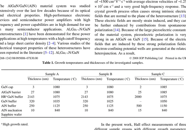
The resistivity and Hall effect measurements of Al0.25Ga0.75N/GaN/AlN heterostructures were carried out as a function of temperature (20–300 K) and magnetic field (0–1.4 T). Figure 1 shows the temperature dependence of the Hall mobilities and sheet carrier densities at 0.4 T in the temperature range of 20–300 K. At high temperatures, mobility decreases sharply with increasing temperature, while
3 Figure 1. Measured Hall mobilities and sheet carrier densities of the investigated samples (B = 0.4 T).
it is nearly independent of the temperature at low temperatures (below 100 K).
Sheet carrier densities of samples A and B are temperature independent at low and mid-temperatures, but with increasing temperature, the sheet carrier density values increase due to the thermal activation of bulk carriers. On the contrary, the sheet carrier density of sample C is essentially temperature independent for the studied temperature interval.
These behaviors of the sheet carrier density and mobility are typical of 2DEG structures. Above 100 K, Hall mobility decreases with increasing temperature with a temperature dependence of ∼T−3/2, which is a typical temperature dependence of phonon scattering mobility. At room temperature, Hall mobilities and sheet carrier densities of samples A, B and C are 687 cm2 V−1 s−1, 409 cm2 V−1 s−1, 1183 cm2 V−1 s−1 and 2.96 × 1013 cm−2, 4.15 × 1013 cm−2, 9.74 × 10¹²
cm−2, respectively. At 20 K, electron mobilities are as high as 3693 cm2 V−1 s−1, 2358 cm2 V−1 s−1 and 4737 cm2 V−1 s−1.
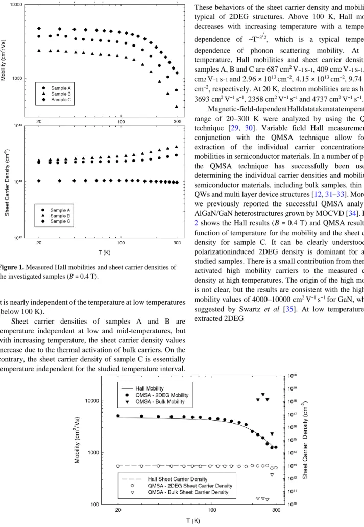
Magnetic-field-dependentHalldatatakenatatemperature range of 20–300 K were analyzed by using the QMSA technique [29, 30]. Variable field Hall measurements in conjunction with the QMSA technique allow for the extraction of the individual carrier concentrations and mobilities in semiconductor materials. In a number of papers, the QMSA technique has successfully been used in determining the individual carrier densities and mobilities in semiconductor materials, including bulk samples, thin films, QWs and multi layer device structures [12, 31–33]. Moreover, we previously reported the successful QMSA analysis of AlGaN/GaN heterostructures grown by MOCVD [34]. Figure
2 shows the Hall results (B = 0.4 T) and QMSA results as a function of temperature for the mobility and the sheet carrier density for sample C. It can be clearly understood that polarizationinduced 2DEG density is dominant for all the studied samples. There is a small contribution from thermally activated high mobility carriers to the measured carrier density at high temperatures. The origin of the high mobility is not clear, but the results are consistent with the high bulk mobility values of 4000–10000 cm2 V−1 s−1 for GaN, which is suggested by Swartz et al [35]. At low temperatures, the extracted 2DEG
Semicond. Sci. Technol. 23 (2008) 095008 S B Lisesivdin et al
4 Figure 3. Mobility versus sheet carrier density at 300 K. Dotted lines represent the sheet resistance contours. Measured values and extracted values for 2DEG (filled symbols) and 2DHG species (empty symbol) using QMSA are shown with in the boxes.
mobility is slightly higher than the measured mobility. Below 100 K, 2DEG mobility is temperature independent. Above 100 K, the 2DEG mobility is limited by lattice scattering mechanisms. The extracted 2DEG density is independent of temperature for the entire studied temperature range, as was expected. The mobilities and densities of the bulk carriers are strongly temperature dependent. The thermally activated bulk carriers mostly originated from the donor levels of the bulk GaN buffer layer [36]. The same analyses were performed for all three samples. All the samples have 2DEG and a bulk electron carrier, and have a hole species that can be a 2D hole gas (2DHG) formation at the GaN/AlN interface that is not shown in figure 2. These hole species can also explain the difference between measured values and the extracted values of 2DEG. In systems such as samples A and B, at low temperatures, the measured conductivities are the sums of 2DEG conductivity and 2DHG conductivity. Mobility and sheet carrier density behaviors are typical of 2D systems. Because of this typical 2D behavior, one may take the measured Hall data as a 2DEG-only data. Singlefield Hall effect measurements extract only averaged mobility and carrier density, in which single-field measurements are used to determine the carrier density and impurity activation energies, and to describe the scattering process that is involved in the case of single-carrier conduction in the investigated semiconductor. In the presence of more than one conduction mechanism, there is often a lack of appreciation of the systematic errors when making these measurements and pitfalls in their interpretation and analysis, since, in these measurements; it is assumed that all of carriers have the same carrier mobility and drift velocity [34, 37].
Therefore, extracting the required data using QMSA or similar mobility spectrum analysis methods is important. A detailed analysis of the probable 2DHG formation is given in our other study [38]. In this study, we mostly focus on a 2DEG
formation at the Al0.25GaN0.75/GaN interface. Figure 3 shows the mobilities of 2DEG (filled symbols) and 2DHG (empty symbols) species versus Ns at 300 K. In samples A and B, there
are strong 2DHG formations. Because of these formations, the measured values show completely different characteristics with respect to the extracted values using the QMSA technique. In contrast, the measured value of sample C was nearly the same with the extracted value using the QMSA technique. The QMSA technique cannot extract a 2DHG formation at this temperature for sample C. Even at low temperatures, sample C has a 2DHG formation only with ∼1– 5 × 1010 cm−2 of the sheet carrier density values. Because of the low 2DHG density, the extracted electron values were nearly the same with the measured values.
Roomtemperature(RT)(300K)andlowtemperature(LT) (20 K) mobilities, sheet carrier densities and conductivities of the electron species of the investigated samples that were obtained by using the QMSA technique are shown in table 2. It can be easily seen that the electrical properties of samples A and C show some similarities at both RT and LT. Sample B has the highest mobility at room temperature and the lowest mobility at low temperatures. Overall, sample B is the worst conductive sample of all.
To investigate these results in more detail, we apply scattering analyses to the extracted 2DEG carrier data. The detailed structure of these analyses is given in our recent study [39]. In summary, the experimental results are compared with the theory, which involved the simple analytical formulae used to calculate the mobility limitations of a number of scattering mechanisms for a 2DEG confined in a pseudotriangular well. In the study, polar-optical phonon (PO), acoustical phonon (AC) (consisting of deformation potential and piezoelectric scatterings), background impurity (IMP), alloy (AL), and interface roughness (IFR) scatterings were all considered. However, the relaxation-time approximation is applicable to elastic or nearly elastic scattering events such as impurity scattering, in which it can also be used for the optic phonon scattering that is highly inelastic [40]. There are some studies about the application of these scattering mechanisms to GaN-based systems [28, 41,
42]. Mobilities that are limited by these individual scattering mechanisms have been calculated from the expressions given in our recent study [39] by using the material parameters shown in table 3 [42, 43]. In the calculation, for the temperature-independent scattering mechanisms AL, IMP and IFR, parameters of Al mole fraction (x), the background impurity (nimp) and lateral size () were taken as 0.25 × 10⁻²³ m−3 [44] and 2.58 × 10⁻¹⁰ m (one monolayer) [43], respectively. The other parameters such as the well width (Z0), deformation potential constant (Ed) and correlation length () were used as adjustable parameters. Here, the pseudotriangular quantum well width can be accepted as a depth of the 95% probability of an electron from the point where the wavefunction penetrates into the AlGaN barrier,
5
and into the GaN layer [45]. Using the Matthiessen’s rule, the
total mobility is then calculated as the combination of individual mobilities.
In figure 4, the fit of the sum of the individual scattering mechanisms to temperature-dependent mobilities that were obtained through QMSA is shown. According to figure 4, optical phonon scattering is the dominant scattering mechanism for temperatures above 200 K. For samples A
Table 3. Material constants of GaN used in scattering calculations [41, 42].
High-frequency dielectric constant ε∞ = 5.35
Static dielectric constant εs = 8.9
Electron effective mass m∗ = 0.22m 0
LO-phonon energy hω¯ = 0.092 eV LA-phonon velocity ul = 6.56 × 10³ ms−1
Density of crystal ρ = 6.15 × 10³ kgm−3
Electron wave vector k = 7.3 × 10⁸ m−1
The electromechanical K2 = 0.039 coupling coefficient
LA elastic constant cLA = 2.650 × 10¹¹ Nm−2 TA elastic
constant cTA = 0.442 × 10¹¹ Nm−2
Alloy mole fraction x = 0.25
Lattice constant in the c = 5.185 × 10⁻¹⁰ m
(0001) direction Volume of one atom
Alloy potential UAL = 2.36 × 10⁻¹⁹ V
and C, alloy scattering is the most dominant scattering mechanism at temperatures lower than 100 K. Background impurityscatteringistheleastimportantscatteringmechanism for samples A and B. For sample C, background impurity scattering is nearly as important as alloy scattering. Acoustic phonon scattering gains importance at the mid-temperatures for samples A and C, but it is still much less important than optic phonon and alloy scatterings. To understand these behaviors of the scattering mechanism, the fit parameters used in the scattering analyses are shown in table 4.
According to the fits, sample C has a wider QW, which can also affect the background impurity scattering. Wider QW means a larger electron penetration into GaN, so that the electron gas is more influenced by the background impurities Figure 4. Electron mobility as a function of temperature for sample A (a), sample B (b) and sample C (c) obtained through QMSA analysis (filled dots). All of the calculated scattering mechanisms are summed up with Matthiessen’s rule and are shown as µTOT (solid
line).
Table 2. Room temperature (RT) and low temperature (LT) mobilities, sheet carrier densities and conductivities of the investigated samples that were obtained by using the QMSA technique.
Sample A Sample B Sample C
RT Mobility (µ) (cm2 V−1 s−1) 1926 2097 1262
Sheet carrier density (ns) (cm−2)
Sheet conductivity ( ) 4.04 × 10¹² 1.24 × 10⁻³ 1.82 × 10¹² 6.11 × 10⁻⁴ 7.00 × 10¹² 1.41 × 10⁻³ LT Mobility (µ) (cm2 V−1 s−1) 6240 4920 5095 Sheet carrier density (ns) (cm−2) Sheet conductivity ( ) 9.24 × 10¹² 9.23 × 10⁻³ 6.94 × 10¹² 5.46 × 10⁻³ 9.33 × 10¹² 7.61 × 10⁻³
Semicond. Sci. Technol. 23 (2008) 095008 S B Lisesivdin et al
6
of GaN [45]. In a wider well, the total number of impurities will be greater than that of the number of impurities in a narrow well. At low temperatures, these impurities will limit the mobility more effectively. Because of the same QW widths for samples A and B, the mobility limiting values of the background impurity scattering are nearly the same. The increase of the well width can be explained with the effect of the barrier layer thickness [45, 46]. A thicker AlGaN barrier causes more localized electrons near the AlGaN/GaN interface. In addition, sample B, which has a lower deformation potential value than samples A and C, is affected more than samples A and C from the interface roughness scattering. In our investigations, we found a linear relation between the deformation potential and the mobility limited by interface roughness scattering (µIFR ∝ Ed) with a 0.9914 correlation.
Samples A and B have one adjustable growth-related quantity, which is a growth temperature of a GaN buffer. According to the results, sample B has a rougher interface than that of sample A, with a 10 ◦C decrease in the growth temperature of the GaN buffer. Sample C is allowed to be different than samples A and B because of the growth temperaturedifferenceintheGaNbufferandAlNbufferlayers and barrier thickness. As was mentioned above, a decrease in the barrier width will increase the quantum well width, which
7 the mobility values that were obtained through QMSA.
Sample A Sample B Sample C QW width (Z0) (nm) 1.5 1.5 4.0
Deformation potential (Ed) (eV) 7.5 5.0 7.0
Correlation length ( 58.2 27.9 54.7
Mobility limited by IFR scat. (µIFR) (cm2 V−1 s−1) 30060 10345 27957
Mobility limited by IMP scat. (µIMP) (cm2 V−1 s−1) 44029 38708 15994
Interface roughnessa ) 30.20 14.45 28.33
a Small value means rougher.
will increase the effect of the impurity-related scatterings. Sample C has an interface roughness like sample A. This is mostly because of the high growth temperature of the GaN buffer. Logically, sample C must have a less rough interface because of the higher growth temperature of the GaN buffer. However, sample C has a little rougher interface than sample A. This little quantitative inconsistency may be caused by the high growth temperature of an AlN buffer. Therefore, for the interface roughness value of sample C, only its qualitative meaning is explainable with the high-temperature growth of the buffer layers. These buffer growth temperaturedependent roughness results are also consistent with our previous XRD investigation of structures with different GaN buffer growth temperatures [19]. However, the process is strongly temperature dependent and further investigations are required.
4. Conclusion
Hall effect measurements on three unintentionally doped Al0.25Ga0.75N/GaN/AlN heterostructure samples grown by MOCVD were carried out as a function of temperature (20– 300 K) and magnetic field (0–1.4 T). Magnetic-fielddependent Hall data were analyzed by using the QMSA technique. The QMSA technique successfully separated electrons in the 2DEG at the Al0.25Ga0.75N/GaN interface, probable 2DHG at the GaN/AlN interface and other bulk electrons in the structure. RT and LT 2DEG mobility, carrier density and conductivities were compared. For a detailed investigation of the growth parameters of the 2DEG, the scattering analyses of the extracted 2DEG mobilities and carrier densities were performed for all of the samples. Accordingtoscatteringanalysisfits, thefollowingresultswere obtained. (a) A thinner AlGaN barrier layer caused a wider QW at the interface. In wider QWs, 2DEG is more influenced by the background impurities of GaN. (b) We found a linear relation between the deformation potential and the mobility limited by the interface roughness scattering (µIFR ∝Ed) with a 0.9914 correlation. While the interface roughness scattering is not straightforward to the model itself, it can be enhanced by taking account of the deformation potential to the perturbation of the electron confinement energy. Strain relaxation at the
interface causes roughness in GaN-based heterostructures [47]. The roughness at the interface may lead to a change in the lattice vibrations, which cause spatial and temporal fluctuations in the conduction band energies [48]. Because the electrons see these fluctuations as a potential form, which is called a deformation potential, interface roughness may be connected with deformation potential. By investigating the extracted 2DEG carrier of a single AlGaN/GaN interface, we found a relation between the deformation potential and interface roughness for GaN-based heterostructures. (c) Roughness ( ) at the Al0.25Ga0.75N/GaN interface decreases to a minimum 14.45 nm2 (small value means rougher) with the increasing buffer layer growth temperature in the studied samples.
In this study, it is shown that the scattering analyses can be used to investigate the relations between the scattering mechanisms and effects of growth conditions to the scatteringrelated parameters such as well width, deformation potential and roughness. Because these scattering parameters are largely used in many studies, it is important to reliably determine the values for different cases. However, these parameters are strongly dependent on the temperature and growthconditions, inwhichfurtherinvestigationsarerequired.
Acknowledgments
This work is supported by the State of Planning Organization of Turkey under Grant no. 2001K120590 and by TUBITAK under Project nos. 104E090, 105E066 and 105A005. One of the authors (Ekmel Ozbay) acknowledges partial support from the Turkish Academy of Sciences.
References
[1] Wu Y F, Keller B P, Keller S, Kapolnek D, Kozodoy P, Denbaars S P and Mishra U K 1996 Appl. Phys. Lett.
69 1438
[2] Wu Y F, Keller B P, Fini P, Keller S, Jenkins T J, Kehias L T, Denbaars S P and Mishra U K 1998 IEEE Electron Device
Lett. 19 50
[3] Li R, Cai S J, Wong L, Chen Y, Wang K L, Smith R P, Martin S C, Boutros K S and Redwing J M 1999 IEEE
Electron Device Lett. 20 323
[4] Chumbes E M, Smart J A, Prunty T and Shealy J R 2001
Semicond. Sci. Technol. 23 (2008) 095008 S B Lisesivdin et al
8
Trans. Electron Devices 48 416
[5] Wong L W, Cai S J, Li R, Wang K, Jiang H W and Chen M 1998 Appl. Phys. Lett. 73 1391
[6] Gaska R, Shur M S, Bykhovski A D, Orlov A O and Snider G L 1999 Appl. Phys. Lett. 74 287 [7] Shen B, Someya T, Nishioka M and Arakawa Y 1999 Phys. Status
Solidi b 216 755
[8] Shen B, Someya T and Arakawa Y 2000 Appl. Phys. Lett.
76 2746
[9] Antoszewski J, Gracey M, Dell J M, Faraone L, Fisher T A, Parish G, Wu Y-F and Mishra U K 2000 J. Appl. Phys.
87 3900
[10] Gokden S 2003 Turk. J. Phys. 27 205
[11] Cordier Y, Hugues M, Lorenzini P, Semond F, Natali F and Massies J 2005 Phys. Status Solidi c 2 2720
[12] Biyikli N, Xie J, Moon Y-T, Yun F, Stefanita C-G, Bandyopadhyay S, Morkoc H, Vurgaftman I and Meyer J R
2006 Appl. Phys. Lett. 88 142106
[13] Anderson D R, Babiker M, Bennett C R, Zakhleniuk N A and Ridley B K 2001 J. Phys.: Condens. Matter 13 5999
[14] Bernardini F and Fiorentini V 1997 Phys. Rev. B 56 R10024
[15] Asbeck P M, Yu E T, Lau S S, Sullivan G J, Hove J V and Redwing J 1997 Electron. Lett. 33 1230
[16] Ambacher O et al 1999 J. Appl. Phys. 85 3222
[17] Bougrioua Z, Moerman I, Nistor L, van Daele B, Monroy E, Palacios T, Calle F and Leroux M 2003 Phys. Status Solidi a
195 93
[18] Miyoshi M, Egawa T and Ishikawa H 2005 J. Vac. Sci.
Technol. B 23 1527
[19] Yu H, Ozturk M K, Ozcelik S and Ozbay E 2006 J. Cryst.
Growth 293 273
[20] Hubbard S M, Zhao G, Pavlidis D, Sutton W and Cho E 2005
J. Cryst. Growth 284 297
[21] Wetzel C, Suski T, Ager J W III, Weber E R, Haller E E, Fischer S, Meyer B K, Molnar R J and Perlin P 1997 Phys.
Rev. Lett. 78 3923
[22] Arulkumaran S, Egawa T, Ishikawa H and Jimbo T 2002
Appl.
Phys. Lett. 81 3073
[23] Heying B, Tarsa E J, Elsass C R, Fini P, DenBaars S P and Speck J S 2001 J. Appl. Phys. 90 5196
[24] Akasaki I, Amano H, Koide Y, Hiramatsu K and Sawaki N 1989 J. Cryst. Growth 98 209 [25] Sasaki T and Matsuoka T 1995 J. Appl. Phys. 77 192 [26] Yu H, Caliskan D and Ozbay E 2006 J. Appl. Phys.
100 033501
[27] Zhang Y and Singh J 1999 J. Appl. Phys. 85 587
[28] Antoszewski J, Gracey M, Dell J M, Faraone L and Fisher T A 2000 J. Appl. Phys. 87 3900
[29] Antoszewski J and Faraone L 2004 Optoelectron. Rev. 12 347 [30] Kelley B J, Dodrill B C, Lindemuth J R, Du G and Meyer J R 2000 Solid State Technol. 12 130
[31] Dodrill B C, Lindemuth J R, Kelley B J, Du G and Meyer J R 2001 Compound Semicond. 7 58
[32] Antoszewski J, Faraone L, Vurgaftman I, Meyer J R and Hoffman C A 2004 J. Electron. Mater. 33 673
[33] Umana-Membreno G A, Parish G, Nener B D, Buttari D, Keller S and Mishra U K 2007 Phys. Status Solidi b
244 1877
[34] Lisesivdin S B, Yildiz A, Acar S, Kasap M, Ozcelik S and
Ozbay E 2007 Appl. Phys. Lett. 91 102113
[35] Swartz C H, Tompkins R P, Myers T H, Look D C and Sizelove J R 2004 J. Electron. Mater. 33 412
[36] Dziuba Z, Antoszewski J, Dell J M, Farone L, Kozodoy P, Keller S, Keller B, Denbaars S P and Mishra U K 1997
J. Appl. Phys. 82 2996
[37] Wolkenberg A, Przeslawski T, Kaniewski J and Reginski K 2003 J. Phys. Chem. Solids 64 7
[38] Acar S, Lisesivdin S B and Kasap M 2008 Thin Solid Films
516 2041
[39] Lisesivdin S B, Acar S, Kasap M, Ozcelik S, Gokden S and Ozbay E 2007 Semicond. Sci. Technol. 22 543
[40] Morkoc H and Nitride 1998 Semiconductors and Devices (Berlin: Springer) p 234
[41] Shur M, Gelmont B and Asif Khan M 1996 J. Electron.
Mater. 25 777
[42] Zanato D, Gokden S, Balkan N, Ridley B K and Schaff W J 2004 Semicond. Sci. Technol. 19 427
[43] Gokden S 2003 Phys. Status Solidi a 2 369
[44] Zhang G Y, Tong Y Z, Yang Z J, Jin S X, Li J and Gan Z Z 1997 Appl. Phys. Lett. 71 3376
[45] Lisesivdin S B, Yildiz A and Kasap M 2007 Opt. Adv.
Mater.-Rapid Commun. 1 467
[46] Balkan N, Gupta R, Cankurtaran M, Celik H, Bayrakli A, Tiras E and Arikan M C 1997 Superlatt.
Microstruct. 22 263
[47] Bourret A, Adelmann C, Daudin B, Rouviere J L, Feuillet G` and Mula G 2001 Phys. Rev. B 63 245307
[48] Singh J 1995 Semiconductor Optoelectronics (New York: McGraw-Hill) p 130
![Table 3. Material constants of GaN used in scattering calculations [41, 42].](https://thumb-eu.123doks.com/thumbv2/9libnet/5772037.117047/6.892.120.826.112.521/table-material-constants-gan-used-scattering-calculations.webp)
