Growth of high crystalline quality semi-insulating GaN layers for high electron mobility
transistor applications
Hongbo Yu, Deniz Caliskan, and Ekmel Ozbay
Citation: Journal of Applied Physics 100, 033501 (2006); doi: 10.1063/1.2221520 View online: http://dx.doi.org/10.1063/1.2221520
View Table of Contents: http://aip.scitation.org/toc/jap/100/3
Published by the American Institute of Physics
Articles you may be interested in
Growth of Fe doped semi-insulating GaN by metalorganic chemical vapor deposition
Applied Physics Letters 81, 439 (2002); 10.1063/1.1490396
Polarization effects, surface states, and the source of electrons in AlGaN/GaN heterostructure field effect transistors
Applied Physics Letters 77, 250 (2000); 10.1063/1.126940
Semi-insulating C-doped GaN and high-mobility AlGaN/GaN heterostructures grown by ammonia molecular beam epitaxy
Applied Physics Letters 75, 953 (1999); 10.1063/1.124252
On the physical operation and optimization of the p-GaN gate in normally-off GaN HEMT devices
Applied Physics Letters 110, 123502 (2017); 10.1063/1.4978690
Electrical and optical properties of Fe-doped semi-insulating GaN templates
Applied Physics Letters 83, 3314 (2003); 10.1063/1.1621458
Role of carbon in GaN
Growth of high crystalline quality semi-insulating GaN layers for high
electron mobility transistor applications
Hongbo Yua兲and Deniz Caliskan
Nanotechnology Research Center, Bilkent University, Bilkent, 06800 Ankara, Turkey
Ekmel Ozbay
Nanotechnology Research Center, Bilkent University, Bilkent, 06800 Ankara, Turkey; Department of Physics, Bilkent University, Bilkent, 06800 Ankara, Turkey; and Department of Electrical and Electronics Engineering, Bilkent University, Bilkent, 06800 Ankara, Turkey
共Received 15 December 2005; accepted 6 June 2006; published online 1 August 2006兲
Semi-insulating character共sheet resistivity of 3.26⫻1011⍀/sq兲 of thick GaN layers was developed for AlGaN / GaN high electron mobility transistor 共HEMT兲 applications on an AlN buffer layer. Electrical and structural properties were characterized by a dark current-voltage transmission line model, x-ray diffraction, and atomic force microscope measurements. The experimental results showed that compared to semi-insulating GaN grown on low temperature GaN nucleation, the crystal quality as well as surface morphology were remarkably improved. It was ascribed to the utilization of a high quality insulating AlN buffer layer and the GaN initial coalescence growth mode. Moreover, the significant increase of electron mobility in a HEMT structure suggests that this is a very promising method to obtain high performance AlGaN / GaN HEMT structures on sapphire substrates. © 2006 American Institute of Physics.关DOI:10.1063/1.2221520兴
I. INTRODUCTION
III-nitride based high electron mobility transistor 共HEMT兲 has exhibited great potential for high-frequency and high-power applications. One key technique in achieving this kind of electrical device is the deposition of thick semi-insulating 共SI兲 GaN layers, in order to ensure proper drain-source current saturation, complete channel pinchoff, and low loss at high frequencies.1However, it is well known that the usual undoped GaN epilayers exhibit an n-type back-ground. This effect is particularly evident in GaN that is grown on sapphire, which is the most commonly used sub-strate for the growth of III-nitride due to its low price, sta-bility at high temperatures, and its mature growth technol-ogy. The origination of the n-type background is still unclear at present. It is reported that the SI GaN can be achieved on sapphire substrate by means of C, Fe, or Zn doping and the control of the initial growth procedures.2–8 However, the high-resistance characteristic is achieved due to the compen-sating acceptor levels that are introduced through deep-level acceptor, edge-type threading dislocations 共TDs兲, or other defects. The existence of additional deep traps is responsible for the leakage current and trapping effect, that may ad-versely affect the device reliability in AlGaN / GaN HEMT.9 Therefore, it is quite important to develop a technique that can obtain a thick SI GaN layer without degrading the crys-talline quality.
In this paper, we report the integration of the GaN epi-growth with a high quality AlN buffer layer. 2m thick SI GaN was grown on AlN template/sapphire substrate by the metal-organic chemical vapor deposition 共MOCVD兲 tech-nique. Based on electrical and structural studies, SI electrical properties 共sheet resistivity of 3.26⫻1011 ⍀/sq兲 as well as
better crystalline quality of GaN were achieved, when com-pared to the normal GaN grown on sapphire by the two-step method.
II. EXPERIMENT
The III-nitride epilayers were grown on c-plane sapphire 共Al2O3兲 substrates in a low pressure MOCVD reactor. Stan-dard trimethylgallium 共TMGa兲, trimethylaluminum 共TMAl兲, and ammonia were used as Ga, Al, and N precursors, respec-tively. Three GaN samples were grown using different pro-cedures: sample A was grown on 0.5m high temperature 共HT兲 AlN buffer, while samples B and C were grown on low temperature共LT兲 GaN nucleation layers 共NLs兲, in which the nucleation and anneal processes were different. Prior to the epilayer growth, the sapphire substrates were cleaned in H2 ambient at 1100 ° C for 10 min. For sample A, a 15 nm thick LT AlN NL was grown at 840 ° C. The temperature was then ramped to 1150 ° C and the sample was annealed at this tem-perature for 2.5 min. This was followed by the growth of a 0.5m HT AlN buffer layer. This structure was used as a template for growth of a 2.0m thick undoped GaN layer. For comparison, a high-resistance GaN layer was also grown on LT GaN NL 共sample B兲. This high-resistance GaN was achieved by calibrating the thicknesses of LT-NL and the HT annealing process carefully.1,5Sample C was grown as a ref-erence sample by using the standard two-step growth condi-tions. The growth parameters of the HT GaN main layer were kept constant for all of the samples.
High resolution x-ray diffraction 共XRD兲 and atomic force microscope 共AFM兲 measurements were carried out to characterize the crystalline quality of the epitaxial layers. The sheet resistivities of the high-resistance GaN layers were measured by an HP 4142B semiconductor parameter ana-lyzer using the transmission line method 共TLM兲. The TLM
a兲Electronic mail: [email protected]
patterns consisted of a set of 200⫻100m2pads with space in the 5 – 50m range. A thin共25 nm兲 Al0.3Ga0.7N layer was grown on the SI GaN samples. The presence of two-dimensional electron gas at the AlGaN / GaN interface en-sures an Ohmic contact, as proposed in Ref. 2. The Ohmic contacts were prepared by the deposition of Ti/ Al/ Ni/ Au 共100 Å/400 Å/100 Å/400 Å兲. After this, the AlGaN layer between the contacts was etched off with reactive ion etch-ing. In situ interferometry was used to monitor the growth process and to measure the growth rate for each sample.
III. RESULTS AND DISCUSSIONS
A symmetric / 2 x-ray diffractometer was used to evaluate the structure of the as-grown GaN layer on an AlN buffer from 20° to 85° diffraction angles. As can be seen in Fig. 1, sharp sapphire peaks can be used as a reference sig-nal. Strong GaN 共002兲 and AlN 共002兲 peaks are displayed approximately at the 34.5° and 36°, respectively, as well as high indices, such as GaN 共004兲 and AlN 共004兲. No other plane reflections were detected. After optimization, the AlN layer exhibited narrow full width at half maximum共FWHM兲 for both rocking and/ 2 scan peaks: 323 arc sec for rock-ing scan and 298 arc sec for/ 2 scan, respectively.10
Figure 2 shows the I-V characteristics of GaN grown on AlN buffer obtained from a set of TLM pads. After rapid thermal annealing at 750 ° C for 1 min, the linearity of I-V curves was obtained for all the TLM pads. At a bias of 10 V, the dark remains about 2⫻109A between two TLM pads separated by a 5 m gap. The I-V characteristics demon-strate that a GaN layer grown on AlN buffer/sapphire sub-strate exhibits a semi-insulating character with calculated
sheet resistivity of 3.26⫻1011⍀/sq, which was one order of magnitude higher than the previous reported results in the literature.1
Table I summarizes the sheet resistivity and FWHM of XRD peaks from different samples. The rocking scans were measured around the共002兲 and 共102兲 reflections of the GaN layers. Samples A and B show SI electrical properties, with sheet resistivities of 3.26⫻1011and 2.7⫻1011⍀/sq, respec-tively. The normally undoped GaN layer共sample C兲 shows an n-type background with sheet resistivity of 9.77 ⫻103⍀/sq 共electron concentration of 1.6⫻1016cm−3兲. We suspected that the n-type background of GaN grown on sap-phire is not due to the impurity incorporation during HT growth, because the growth parameters of the HT-GaN main layer were kept constant for the SI GaN and normal GaN. It is most likely that the n-type background of GaN epilayers is originated from the sapphire substrate or the LT-GaN nucle-ation growth process. During the initial growth stage, oxygen can move into the GaN layer by thermal etching and/or dif-fusion, which results in a highly conducting channel near the sapphire interface.11,12So there are two main ways to obtain SI electrical character of GaN grown on sapphire substrate: 共i兲 intentional introduction of acceptor-type level in the band gap to compensate the n-type background. However, this method may also result in high density of defects in the epilayers; 共ii兲 insertion of insulating layer to block off the effect from sapphire substrate which acts as the oxygen source. The electrical character and crystal quality of subse-quent GaN epilayer is influenced by the characteristic of in-sulating material definitively.
XRD symmetric 共002兲 incorporated with asymmetric 共102兲 scan is a reliable technique to characterize the crystal quality of GaN films. The defects within the structure of sample B cause significant broadening in both the symmetric
FIG. 2.共Color online兲 Dark I-V characteristics of sample A obtained from a set of TLM pads.
FIG. 1. XRD/ 2scan of sample A.
TABLE I. Sheet resistivities and FWHM of XRD peaks from different samples.
Sample
Nucleation
Layer Buffer layer
Sheet resistivity
共⍀/sq兲 scanFWHM of rocking共0002兲 共arc sec兲
FWHM of rocking scan共10-12兲 共arc sec兲
A LT-AlN HT-AlN 3.26⫻1011 234 280
B LT-GaN No 2.7⫻1011 360 1026
C LT-GaN No 9.77⫻103 256 312
共002兲 and asymmetric 共102兲 rocking curves, which have fit-ted widths of 360 and 1026 arc sec, respectively. It is note-worthy that the measured width of the共102兲 rocking curve from sample B is strikingly larger than that of the 共002兲 rocking curve. The dramatic broadening of the asymmetric diffractions compared to the symmetric diffractions is indica-tive of a defecindica-tive structure with a large pure edge TD con-tent, since the 共002兲 peak is only broadened by screw or mixed TD while the 共102兲 peak is broadened by all of the TDs.13 For sample B, it is very likely that the high-density edge-type TDs compensate the background of GaN, leading to the SI electrical character. The 共002兲 and 共102兲 rocking curves have fitted widths of 234 and 280 arc sec for sample A, and 256 and 312 arc sec for sample C, respectively. Com-pared to that of sample B, sample A has remarkably narrower peak widths for both共002兲 and 共102兲 reflection planes indi-cating a significant improvement of crystalline quality. The narrow 共102兲 peak width of SI sample A means that factors other than edge-type TDs are responsible for the SI electrical character. It is noted that both the 共002兲 and 共102兲 peak widths of sample A are narrower than that of sample C, which was grown using a normal two-step method. We as-cribe the crystal quality improvement to the GaN layer grown on high quality AlN buffer layer not on LT-NL di-rectly.
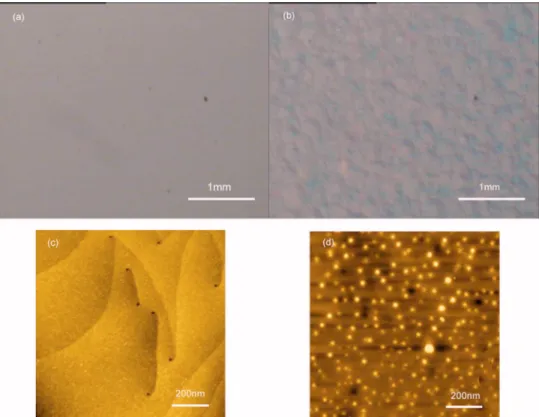
Figure 3 is the surface image of an as-grown GaN epil-ayer taken by a Nomarski optical microscopy in order to compare the optical macroscopic morphology between samples A and B. Compared to the mirrorlike surface of sample A关Fig. 3共a兲兴, the surface image of sample B shows an obvious bumpy surface morphology 关Fig. 3共b兲兴, which appears as craterlike defects. In order to further study the surface morphology of samples A and B, an AFM measure-ment was carried out in a 1⫻1m2 area of the as-grown
GaN layers. Sample A features a smooth surface morphology delineated by steps, terraces, and dark spots关Fig. 3共c兲兴 with the root mean square共rms兲 of 0.25 nm. In contrast, sample B 关Fig. 3共d兲兴 is dominated by pits and a high density 共3 ⫻1010/ cm2兲 of raised islandlike structures of various sizes 共up to 60 Å high兲 with the rms of 0.36 nm. So any trace of underlying steps and terraces was washed out on the AFM map. The image of sample A shows a surface morphology with lots of terraces, which have a height of 0.3 nm corre-sponding to one monolayer of 共002兲 GaN. Most of the ter-races are pinned by small dark spots with a density of about 8⫻108/ cm2. Step terminations on a single crystal surface must correspond to the intersection of a pure screw or mixed screw-edge threading dislocation with the free surface. The surface terraces suggest that a typical two-dimensional共2D兲 step-flow growth mode basically dominates the GaN growth of sample A, which is entirely different from that of sample B. A HT-AlN buffer and LT-GaN nucleation high-resistance GaN templates were used to grow Al0.3Ga0.7N / AlN / GaN HEMT structures with 25 nm AlGaN and 2 nm AlN barriers. Hall-effect measurements were performed on both samples at room temperature. The mobilities of the HT-AlN buffer and LT-GaN nucleation samples were 1700 and 1260 cm2/ V s, respectively 共sheet charge was 1.3 ⫻1013cm−2for both samples兲. As can be seen, the improved surface quality of the HT-AlN sample leads to evidently higher values of the mobility.
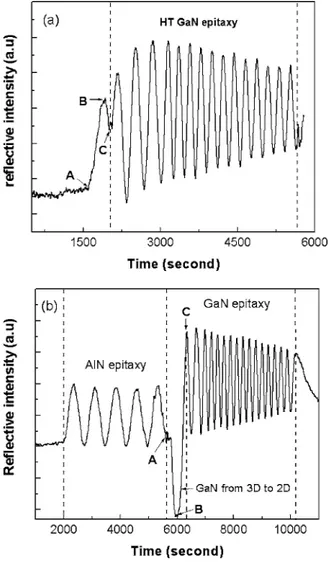
In situ reflectance can be used to relate the growth
mechanisms to the sheet resistance and crystal quality. Fig-ure 4 shows the reflectance traces of samples B and A during the epigrowth. As shown in Fig. 4, the LT-NL growth of sample B is from point A to point B, and then the reactor temperature is ramped to HT for annealing. Growth of the main HT-GaN layer begins at point C. By controlling the
FIG. 3. 共Color online兲 Nomarski opti-cal microscope and 1⫻1m2 area
AFM images of as-grown GaN surface for关共a兲 and 共c兲兴 sample A and 关共b兲 and 共d兲兴 sample B.
thickness of NL, annealing temperature, and annealing time, the 2D growth mode begins almost immediately after the onset of HT growth. The edge-type TDs cannot be bent by these processes, which collide with the rules of achieving high crystal quality GaN with a smooth surface. As shown in Fig. 4共b兲, the growth of the main GaN is from point A, and the reflectance is decreased during the initial stage 共from points A to B兲 of HT GaN growth due to the three-dimensional 共3D兲 islandlike growth. It is ascribed to the 2.4% lattice mismatch between GaN and AlN. As the islands begin to coalesce growth 共quasi-2D growth兲, the reflectance will begin to increase共from points B to C兲. It is reported that
the longer coalesce time共from 3D-2D growth兲 enables more of the edge-type TDs to annihilate each other with 90° bending.14Compared to the growth process of sample B, the initial 3D-2D growth mode of sample A can decrease the density of TDs and improve crystal quality, which is consis-tent with the material characterization results.
IV. SUMMARY
In summary, we have demonstrated the MOCVD growth of thick high-resistance GaN layers on sapphire substrate by inserting an AlN buffer layer. The SI character 共sheet resis-tivity of 3.26⫻1011⍀/sq兲 of GaN can be achieved with high crystal quality and step-flow surface morphology. It was ascribed to the utilization of a high quality insulating AlN buffer layer and the GaN initial coalescence growth mode. The HEMT structure was grown based on this kind of SI GaN / AlN buffer. Hall measurement reveals that this is a very promising method to obtain high performance AlGaN / GaN HEMT on sapphire substrate.
ACKNOWLEDGMENTS
This work was supported by EU-DALHM, EU NOE-METAMORPHOSE, EU NOE-PHOREMOST, TUBITAK-NANOTR, and TUBITAK under Project Nos. 104E090 and 105E066. One of the authors 共E.O.兲 acknowledges partial support from Turkish Academy of Sciences.
1S. M. Hubbard, G. Zhao, D. Pavlidis, W. Sutton, and E. Cho, J. Cryst.
Growth 284, 297共2005兲.
2S. Heikman, S. Keller, S. P. DenBaars, and U. K. Mishra, Appl. Phys. Lett.
81, 439共2002兲.
3J. B. Webb, H. Tang, S. Rolfe, and J. A. Bardwell, Appl. Phys. Lett. 75,
953共1999兲.
4A. Y. Polyakov, N. B. Smirnov, A. V. Govorkov, and S. J. Pearton, Appl.
Phys. Lett. 83, 3314共2003兲.
5Z. Bougrioua, I. Moerman, L. Nistor, B. Van Daele, E. Monroy, T.
Pala-cios, F. Calle, and M. Leroux, Phys. Status Solidi A 195, 93共2003兲.
6J.-H. Lee, M.-B. Lee, S.-H. Hahm, Y.-H. Lee, J.-H. Lee, Y.-H. Bae, and H.
K. Cho, MRS Internet J. Nitride Semicond. Res. 8, 5共2003兲.
7N. I. Kuznetsov, A. E. Nikolaev, I. P. Nikitina, and V. A. Dmitriev, Appl.
Phys. Lett. 75, 3138共1997兲.
8A. Y. Polyakov, A. V. Govorkov, N. B. Smirnov, A. E. Nikolaev, I. P.
Nikitina, and V. A. Dmitriev, Solid-State Electron. 45, 249共2001兲.
9D. S. Green, S. R. Gibb, B. Hosse, R. Vetury, D. E. Grider, and J. A.
Smart, J. Cryst. Growth 272, 285共2004兲.
10H. B. Yu, E. Ulker, and E. Ozbay, J. Cryst. Growth共accepted兲. 11D. C. Look and R. J. Molnar, Appl. Phys. Lett. 70, 3377共1997兲. 12M. G. Cheong et al., Appl. Phys. Lett. 77, 2557共2000兲.
13B. Heying, X. H. Wu, S. Keller, Y. Li, D. Kapolnek, B. P. Keller, S. P.
DenBaars, and J. S. Speck, Appl. Phys. Lett. 68, 643共1996兲.
14J. Chen, J. Cryst. Growth 254, 348共2003兲.
FIG. 4. Reflectivity monitored during semi-insulating GaN epitaxy on共a兲 LT-GaN nucleation and 共b兲 AlN buffer. The 3D-2D transition is clearly visible in GaN grown on AlN buffer.