Abstract— In this work, the deposition of 3-nm dispersed Zinc-Oxide (ZnO) nanislands by thermal Atomic Layer Deposition (ALD) is demonstrated. The physical and electronic properties of the islands are studied using Atomic Force Microscopy, UV-Vis-NIR spectroscopy, and X-ray Photoelectron Spectroscopy. The results show that there is quantum confinement in 1D in the nanoislands which is manifested by the increase of the bandgap and the reduction of the electron affinity of the ZnO islands. The results are promising for the fabrication of future electronic and optoelectronic devices by single ALD step.
I. INTRODUCTION
ZnO has lately attracted considerable attention due to its remarkable electrical and optical properties such as its direct bandgap energy of 3.36 eV at room temperature and large exciton binding energy of 60 meV. Atomic Layer Deposition (ALD) has received great attention due to its suitability for the fabrication of conformal material layers with thicknesses down to the nanometer range. However, it was originally thought that in ALD, the self-terminating gas-solid reactions lead automatically to the growth of one atomic or molecular layer of the chosen material per reaction cycle. Only recently it was shown that, because of steric hindrance, the growth-per-cycle (GPC) in ALD can be less than a monolayer when compounds of metals and ligands are used as reactants [1-2].
When GPC is less than a monolayer, islands growth is promoted. In this growth mode, it has been observed a generic stress evolution from compressive to tensile, then back to compressive stress as the film thickened. The tensile stress is attributed to the impingement and coalescence of growing islands: islands strain to close the gap between them and replace the free surfaces with a low energy grain boundary [3], [4]. In this work, ZnO nano-islands are
This work was supported by Masdar Institute of Science and Technology, United Arab Emirates, the Office of Naval Research global grant N62909-16-1-2031, and L’Oréal-UNESCO For Women in Science Middle East Fellowship.
T. G. Ulusoy and A. K. Okyay are with the Institute of Materials Science and Nanotechnology, Bilkent University, 06800 Ankara, Turkey
T. G. Ulusoy, A. Ghobadi, A. Nazirzadeh and A. K. Okyay are with the UNAM-National Nanotechnology Research Center, Bilkent University, 06800 Ankara, Turkey
A. Ghobadi, A. Nazirzadeh and A. K. Okyay are with the Department of Electrical and Electronics Engineering, Bilkent University, 06800 Ankara, Turkey
N. El-Atab, F. I. Chowdhury and A. Nayfeh are with the Institute Center for Microsystems – iMicro, Department of Electrical Engineering and Computer Science (EECS), Masdar Institute of Science and Technology Abu Dhabi, United Arab Emirates.
deposited using thermal ALD and their electronic and physical properties are studied using Atomic Force Microscopy (AFM), UV-Vis-NIR spectrophotometer, and X-Ray Photoelectron Spectroscopy (XPS).
II. FABRICATION OF ZNONANO-ISLANDS
ALD is used to deposit ZnO on highly doped Si (111) and glass samples by alternating pulses of Zn(C2H5)2 (DEZ) and H2O. One ALD cycle consists of the following steps: (1) 0.02s supply of DEZ, (2) 10s N2 purge of excess DEZ and any byproducts, (3) 0.1s supply of H2O, and (4) 10s N2 purge of excess H2O and any byproducts.
Fig. 1. ZnO nanoislands topography. (a) 2D AFM image of nanoislands. (b) 3D AFM image of the nanoislands.
Due to reasons like large size precursors, poorly reactive substrate with the reactants used in ALD, deposition at defect sites, short precursor dose duration, etc. nano-islands are formed in Volmer-Weber growth mode [5]. In fact, the
Growth of ~3-nm ZnO Nano-islands Using Atomic Layer
Deposition
Nazek El-Atab, Farsad Imtiaz Chowdhury, Turkan Gamze Ulusoy, Amir Ghobadi, Amin
Nazirzadeh, Ali K. Okyay and Ammar Nayfeh
Proceedings of the 16th International Conference on Nanotechnology Sendai, Japan, August 22-25, 2016
deposition rate is found to be smaller than a single layer per cycle which results in islands growth mode. As the number of cycles is increased, the thickness of the ZnO layer is increased and the islands start to coalesce and form a continuous layer [5]. In this work, the recipe used to deposit ZnO islands consist of 20 ZnO thermal ALD cycles at a pressure of 80 mtorr and a temperature of 180°C. A sample with 18-nm ALD continuous ZnO film is also prepared in order to compare the electronic properties of the two samples. Fig. 1a shows the AFM 2D topography image (500×500 nm2) of the ZnO nanoislands, and Fig. 1b shows a 3D image of the topography. The average thickness of the islands is around ~3-nm while the width of the majority of the islands is below 40-nm.
III. EXPERIMENTAL CHARACTERIZATION AND DISCUSSION
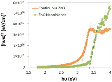
In order to analyze the change in the properties of the ultrathin nanoislands, the transmittance and reflectance spectra of the samples are obtained using a UV-Vis-NIR spectrophotometer, and then the bandgap of the ZnO is obtained by first plotting the Kubelka-Munk function. In fact, the increase in the bandgap of nanostructures as the size is reduced is the most identifiable aspect of quantum confinement in semiconductors [6]. The Kubelka-Munk function is used to extract the bandgap of both samples by plotting (hυα)2 vs. hυ where hυ is the photon energy and α is the absorption coefficient since ZnO is a direct bandgap material. Fig. 2 shows that the bandgap of the 18-nm continuous layer is around 3.1 eV while 3.4 eV for the ZnO nanoislands. However, the extracted values from the Kubelka-Munk plot correspond to a valence band-donor level transition and the true bandgap of ZnO quantum confined in 1D is reposrted to be around 3.62 eV while the bandgap of bulk ZnO is ~3.36-3.4 eV [7]. This increase in bandgap is expected to be due to quantum confinement in 1D in the nanoislands. In fact, when the size of the nanostructures becomes comparable to the Bohr radius of the excitons in ZnO which is around 2.3-nm, then quantum confinement
Fig. 2. Kubelka-Munk plot of the ZnO nanoislands and continuous 18-nm ZnO.
effects occur. Since the nanoislands thickness is 3-nm but the width is much larger (40-nm), then quantum confinement in 1D is expected.
Moreover, X-ray Photoelectron Spectroscopy measurements are conducted on the two samples and the band offsets of the ZnO nanoislands and continuous film on Si are obtained as shown in Fig. 3a and 3b, respectively. Fig. 3 shows that the electron affinity of the nanoislands is reduced which is also an aspect of quantum confinement [8-12]. The reduction of the electron affinity affect the band offsets with Si, which will affect the performance of the devices with embedded ZnO islands. For example, using such nanoislands in memory devices may inhibit the storage of electrons in the ZnO due to the absence of a quantum well formed by the conduction band offsets between ZnO and surrounding oxides (depending on the surrounding oxides electron affinity); however, the reduction of the electron affinity increases the valence band offset which would allow for more energy states for the storage of holes, therefore, a large memory window can be obtained. In addition, such nanoislands can be used as a light trapping scheme for solar cells. Finally, the fabrication of such islands by ALD allows for the fabrication of electronic and optoelectronic devices with embedded nanoislands by single ALD step which would reduce the probability of contamination of the devices.
Fig. 3. a) Band offset of the ZnO nanoislands on Si, b) Band offset of 18-nm continuous ZnO on Si.
IV. CONCLUSIONS
In conclusion, the deposition of 3-nm ZnO nanoislands by thermal ALD is demonstrated. The nanoislands have a width which is smaller than 40-nm and are separated with each other. In addition, quantum confinement in 1D in the ZnO nanoislands is shown by the increase in the bandgap. Moreover, the electron affinity is reduced which affects the band offset with the surrounding materials and therefore 688
affect the performance of the devices that include these nanoislands. The presented results make the nanoislands promising for future electronic and optoelectronic devices to be fabricated by single ALD step.
ACKNOWLEDGEMENTS
We gratefully acknowledge financial support for this work provided by the Masdar Institute of Science and Technology, the Office of Naval Research global grant N62909-16-1-2031, and L’Oréal-UNESCO For Women in Science Middle East Fellowship.
REFERENCES
[1] M. Ylilammi, “Monolayer thickness in atomic layer deposition,”
Thin Solid Films, vol. 279, no. 1–2, pp. 124–130, Jun. 1996.
[2] R. L. Puurunen, “Growth Per Cycle in Atomic Layer Deposition: A Theoretical Model (Chem. Vap. Deposition 2003, 9, 249),”
Chem. Vap. Depos., vol. 10, no. 3, pp. 124–124, Jun. 2004.
[3] W. D. Nix and B. M. Clemens, “Crystallite coalescence: A mechanism for intrinsic tensile stresses in thin films,” J. Mater.
Res., vol. 14, no. 08, pp. 3467–3473, Jan. 2011.
[4] L. B. Freund and E. Chason, “Model for stress generated upon contact of neighboring islands on the surface of a substrate,” J.
Appl. Phys., vol. 89, no. 9, p. 4866, May 2001.
[5] R. L. Puurunen and W. Vandervorst, “Island growth as a growth mode in atomic layer deposition: A phenomenological model,” J.
Appl. Phys., vol. 96, no. 12, p. 7686, Dec. 2004.
[6] H. Yu, et al. "Two-versus three-dimensional quantum confinement in indium phosphide wires and dots," Nature
materials vol. 2, no. 8, pp. 517-520, 2003.
[7] T. G. Ulusoy, A. Ghobadi, and A. K. Okyay, “Surface engineered angstrom thick ZnO-sheathed TiO 2 nanowires as photoanodes for performance enhanced dye-sensitized solar cells,” J. Mater. Chem. A, vol. 2, no. 40, pp. 16867–16876, Sep. 2014.
[8] Ammar Nayfeh, Ali K. Okyay, Nazek El-Atab, Ayse Ozcan, and Sabri Alkis, “Low Power Zinc-Oxide Based Charge Trapping Memory with Embedded Silicon Nanoparticles,” Invited, 226th ECS meeting 2014, no. 46, p. 2143-2143, Cancun, Mexico, October 5-10, 2014.
[9] N. El-Atab, et al. “Memory effect by charging of ultra-small 2-nm laser-synthesized solution processable Si-nanoparticles embedded in Si-Al2O3-SiO2 structure,” Phys. Status Solidi A, vol. 212, no. 8, pp. 1751–1755, 2015.
[10] N. El-Atab, et al. “Enhanced non-volatile memory characteristics with Quattro-layer graphene-nanoplatelets vs. 2.85-nm Si-nanoparticles with asymmetric Al2O3/HfO2 tunnel oxide,”
Nanoscale Res. Lett., vol. 10, no.1, p. 248, 2015.
[11] Ammar Nayfeh, Ali K. Okyay, Nazek El-Atab, Furkan Cimen, and Sabri Alkis, “Transparent Graphene Nanoplatelets for Charge Storage in Memory Devices,” Invited, 226th ECS meeting 2014, no. 37, p. 1879-1879, Cancun, Mexico, October 5-10, 2014. [12] Nazek El-Atab and Ammar Nayfeh “1D vs. 3D quantum
confinement in 1-5 nm ZnO nanoparticles agglomerations for application in charge trapping memory devices,” Nanotechnology vol. 27, p. 275205, 2016.