THE GROWTH, FABRICATION AND
CHARACTERIZATION OF HIGH PERFORMANCE
Al
xGa
1-xN METAL-SEMICONDUCTOR-METAL
PHOTODIODES
A THESIS
SUBMITTED TO THE DEPARTMENT OF PHYSICS AND INSTITUTE OF ENGINEERING AND SCIENCE
OF BILKENT UNIVERSITY
IN PARTIAL FULFILLMENT OF THE REQUIREMENTS FOR THE DEGREE OF
MASTER OF SCIENCE
By Serkan Bütün September 2006
Prof. Dr. Ekmel Özbay (Supervisor)
I certify that I have read this thesis and that in my opinion it is fully adequate, in scope and in quality, as a dissertation for the degree of Master of Science.
Asst. Prof. H. Volkan Demir
I certify that I have read this thesis and that in my opinion it is fully adequate, in scope and in quality, as a dissertation for the degree of Master of Science.
Asst. Prof. Vakur B. Ertürk
Approved for the Institute of Engineering and Science:
Prof. Dr. Mehmet Baray,
Abstract
THE GROWTH, FABRICATION, AND CHARACTERIZATION OF HIGH PERFORMANCE AlxGa1-xN
METAL-SEMICONDUCTOR-METAL PHOTODIODES Serkan Bütün
M.S. in Physics
Supervisor: Prof. Dr. Ekmel Özbay September 2006
High performance UV photodetectors have attracted unwarranted attention for various applications, such as in military, telecommunication, and biological imaging, as an AlxGa1-xN material system is also rather suitable for such applications. Its direct band gap covers the spectrum from 200 nm to 360 nm by way of changing the Al concentration in the compound. In this present thesis, the design and growth of an Al0.75Ga0.25N template on sapphire substrate and a deep-UV photodiode with a cut off wavelength of 229 nm that was fabricated on the Al0.75Ga0.25N template is presented. A responsivity of 0.53 A/W was attained corresponding to a detectivity of 1.64 × 10¹² cmHz1/2/W at a 50 V bias and 222 nm UV light illumination. The UV/VIS rejection ratio of seven orders of magnitude was achieved from the fabricated devices. The second work that was conducted in this thesis was the growth of a semi-insulating (SI-) GaN template. We also fabricated visible-blind photodetectors on this semi-insulating (SI-) GaN template. Furthermore, we fabricated identical samples on a regular GaN template in order to investigate any possible
improvement. The improvement found was obvious in terms of dark current. A dark current density of 1.96 × 10⁻¹⁰ A/cm2 at a 50 V bias voltage for an SI-GaN photodetector was obtained, which is four orders of magnitude lower than devices on a regular GaN template. Devices on an SI-GaN had very high detectivity, and therefore, SI-GaN was used for low level power detection. The photogenerated current was well above the dark current that was under the illumination of just a few picowatts of UV light.
Keywords: Photodetector, Photodiode, GaN, AlGaN, Metal-semiconductor-metal, Semi-insulating
Özet
YÜKSEK PERFORMANSLI AlxGa1-xN METAL-YARIİLETKEN-METAL FOTODİYOTLARIN BÜYÜTÜLMESİ, ÜRETİLMESİ VE
KARAKTERİZASYONU Serkan Bütün Fizik Yüksek Lisans
Tez Yöneticisi: Prof. Dr. Ekmel Özbay Eylül 2006
Askeri, telekomünikasyon ve biyolojik görüntüleme gibi alanlar için yüksek performanslı mor-ötesi (MÖ) fotodedektörler her zaman önem arz etmektedir. AlxGa1-xN malzeme sistemi bu tür uygulamalar için oldukça uygundur. Malzemenin doğru bant aralığı Al konsantrasyonu değiştirilerek 200 nm den 360 nm ye kadar olan bölge taranabilir. Bu çalışmada tasarımını yapıp safir üzerine büyüttüğümüz Al0.75Ga0.25N katmanını ve bu katman üzerinde ürettiğimiz 229 nm kesme dalgaboyuna sahip derin MÖ fotodiyotları sunuyoruz. Üretilen fotodiyotlardan 50 V gerilim ve 222 nm MÖ ışık altında 0.53 A/W responsivite ve buna karşılık gelen 1.64 × 10¹² cmHz1/2/W dedektivite değerleri ölçüldü. On milyon kat mor-ötesi/görünür kontrastı elde edildi. Bu çalışmamızda değindiğimiz ikinci çalışma ise güneş-körü uygulamalar için düşük karanlık akımlı GaN fotodiyot üretimiydi. Bunun için önce safir üzerine bir yarı-yalıtkan GaN katmanı büyütüldü. Aynı zamanda karşılaştırma amacıyla başka bir GaN katmanı da geleneksel yöntemle büyütüldü. Neticede iki
fotodiyotun karanlık akımları karşılaştırıldı. Yarı yalıtkan malzeme üzerine büyütülen fotodiyotun dört bin kat daha az karanlık akım geçirdiği gözlendi. Bu düşük karanlık akım nedeniyle çok yüksek dedektivite değeri ölçüldü. Bu nedenle fotodiyot çok zayıf ışık sinyalleri altında denendi ve birkaç pW gibi düşük ışık tespit edilebildi.
Anahtar sözcükler: Fotodedektör, Fotodiyot, GaN, AlGaN, Metal-yarıiletken-metal, Yarı-yalıtkan
Acknowledgements
I hereby present my sincere gratitude to my supervisor Prof. Dr. Ekmel Özbay for his endless support, guidance, motivation, and encouragement throughout this research. It was an experience of a lifetime and such a great honor to work with him.
I would like to specifically thank Dr. Mutlu Gökkavas for his help, and the valuable experience and suggestions that he shared with me, Dr HongBo Yu for his help on material growth, Mr. Erkin Ülker and Mr. Deniz Çalışkan for heir valuable assistance on every matter.
I would like to thank all of the former and present personnel of the Nanotechnology Research Center for being great friends, having understanding, and making life much easier for me. My special thanks go to my office colleagues Mr. Turgut Tut and Mr. Bayram Bütün for their help with the laboratory equipment.
I would also like to thank all of the former and present personnel of the Advanced Research Laboratory and the Department of Physics. It was an honor to work alongside these rather hardworking people. Special thanks also go to Mr. Murat Güre and Ergun Kahraman for their technical support and guidance in the laboratory.
I would like to thank Asst. Prof. H. Volkan Demir and Asst. Prof. Vakur B. Ertürk for their being in my thesis committee.
Finally, I am indebted to my wonderful family for their continuous support and care.
Contents
Abstract i Özet iii Acknowledgements v
Contents vi
List of Figures viii
List of Tables x
1 Introduction 1
2 Theory 5
2.1 The Photodiode Operation………... 5
2.2 The Schottky Junction………... 6
2.3 The band gap of AlxGa1-xN……… 8
2.4 Metal-Semiconductor-Metal Photodiodes………. 8
2.5 Photodetector Characterization……….. 10
2.5.1 Current Voltage Characterization……….. 10
2.5.2 Responsivity and Quantum Efficiency……….. 11
2.5.3 Noise and Detectivity………. 12
3 Design and Growth 14 3.1 Metal-Organic Chemical Vapor Deposition (MOCVD)…… 14
3.2 Material Design and Growth……….. 16
3.2.1 Al0.75Ga0.25N Design……….. 16
3.2.2 Al0.75Ga0.25N Growth………. 17
3.2.3 SI- and UD-GaN Wafer Design………. 20
3.2.4 SI- and UD-GaN Wafer Growth……… 23
4 Fabrication 28
4.1 Process Basics……… 28
4.1.1 Sample Preparation……… 29
4.1.2 Photolithography……… 30
4.1.2.1 Positive Photolithography………... 31
4.1.2.2 Image Reversal Photolithography………... 31
4.1.3 Etching………... 31 4.1.3.1 Dry Etching………... 32 4.1.3.2 Wet etching………... 32 4.1.4 Deposition……….. 32 4.1.4.1 Metallization………... 33 4.1.4.2 Dielectric Coating………... 33
4.2 Device Fabrication Steps………... 33
4.2.1 Mesa Isolation……… 33
4.2.2 Schottky Contact Formation……….. 34
4.2.3 Dielectric Coating……….. 35
4.2.4 Interconnect Metallization………. 36
4.2.5 Lift-Off………... 36
5 Measurements 39 5.1 Experimental Results of Deep-UV Photodetectors………… 39
5.1.1 Current vs. Voltage Characteristics………... 39
5.1.2 Quantum Efficiency/Responsivity Measurements…. 41 5.1.3 Noise Characterization………... 43
5.2 Experimental Results of Visible-Blind Photodetectors……. 45
5.2.1 Current vs. Voltage Characteristics………... 45
5.2.2 Responsivity Measurements……….. 46
5.2.3 Low Power Photodetection……… 50
6 Achievements and Future Directions 52
Bibliography 54
List of Figures
2.1 Schematic diagram of a simple photodiode operation………. 6
2.2 Schematic band diagram of a Schottky Contact. (a) before (b) after the contact formation………...……… 7
2.3 Schematic views of an MSM photodetector. (a) cross-sectional view (b) top view………. 9
3.1 Schematic diagram of the MOCVD reactor……… 15
3.2 Schematic diagram of the spectral transmission setup……… 19
3.3 Spectral transmission measurement of the Al0.75Ga0.25N wafer…... 20
3.4 XRD ω/2θ scan of the SI-GaN sample……… 23
3.5 XRD ω/2θ scan of UD-GaN the control sample……….. 24
3.6 Crystal quality improvement of SI-GaN over UD-GaN………….. 24
3.7 Experimental setup of the photoluminescence measurement…….. 25
3.8 PL measurement of the SI-GaN sample………... 26
3.9 PL measurement of the UD-GaN sample……… 26
3.10 PL comparison of the SI-GaN and UD-GaN templates…………... 27
4.1 Sample before (a) and after (b) mesa isolation step………... 34
4.2 Schottky metallization……….. 35
4.3 (a) Sample surface after dielectric coating, (b) Sample surface after wet etching with HF……… 35
4.4 Finalized device………... 36
4.5 Micrographs taken during the fabrication……… 38
5.1 IV Characteristics of a 100 × 100 µm2 area device………... 40
5.2 IV Characteristics of a 4 µm finger width/spacing and 100 × 100 µm2 area device in a semilog scale………. 41 5.3 Schematic diagram of the Quantum efficiency setup………. 42 5.4 Spectral responsivity measurements of a 400 × 400 µm
photodetector……… 43 5.5 Experimental setup for noise measurements………
44 5.6 Spectral noise measurement of a high-leakage 100 × 100 µm
photodetector with varying applied bias voltage………... 45 5.7 Current-voltage characteristics of 200 × 200 µm MSM
photodiodes with 10 µm/10 µm finger width/spacing on two different chips……….. 46 5.8 Schematic diagram for a modulated spectral responsivity
measurement……… 47 5.9 Measured spectral responsivity curves of 200 × 200 µm devices
with 3 µm/3 µm finger width/spacing on a UD-GaN sample…….. 48 5.10 Measured spectral responsivity curves of 200 × 200 µm devices
with 3 µm/3 µm finger width/spacing on SI-GaN sample………... 49 5.11 Normalized modulated photoresponse of a 200 × 200 µm device
with 3 µm/3 µm finger width/spacing on the SI-GaN chip as a function of chopper frequency………. 50 5.12 Measured photocurrent of a 200 × 200 µm device with 3 µm/3 µm
finger width/spacing on the SI-GaN chip as a function of optical power and bias voltage. The dashed lines represent the adjustments to the plotted data………. 51
List of Tables
3.1 Epitaxial design of the Al0.75Ga0.25N wafer……….. 17 3.2 Epitaxial design of the semi-insulating GaN wafer……….. 21 3.3 Epitaxial design of the unintentionally doped GaN wafer……… 21 4.1 Technical data sheet of the MSM photodetector fabrication…… 37
Chapter 1
Introduction
Ultraviolet (UV) spectrum corresponds to electromagnetic radiation with energy that is higher than 3.1 eV. Natural UV sources are mainly very hot objects, such as stars and flames. Developments in the past fifteen years have brought new artificial UV sources such as UV light emitting diodes [1-3] in addition to UV lamps. However, the most significant UV source is the sun. Most of the UV radiation on earth is due to solar radiation. Normally, UV radiation is very harmful to life. Fortunately, the ozone layer absorbs the UV radiation with λ<280 nm, which is called the solar blind region. Therefore, there is no natural radiation for λ<280 nm within the atmosphere. Hence, it is even more important to make a detector that is sensitive for λ<280 nm because the source will be an extraordinarily hot object if there is radiation within the atmosphere [4]. Similarly, the radiation above the visible region of the electromagnetic spectrum is called the visible-blind region (λ<400 nm) because the human eye does not respond to the wavelengths smaller than 400 nm.
These two regions are named after the natural cut offs. There are also standards that are given to the various portions of the UV spectrum such as, near UV (400 nm – 320 nm), mid-UV (320 nm – 260 nm), and deep UV (260 nm – 190 nm). The region below the deep UV portion is called vacuum UV because the atmosphere absorbs below 190 nm.
There are numerous applications of UV generation and detection. For the generation part we have UV LEDs and lasers for UV photolithography, high density optical storage, non-line of sight communication systems, true color displays etc… Detection of the UV spectrum has a wide range of applications such as in the military, environmental, scientific, telecommunication, and industrial areas. For instance, from a scientific point of view, we have chemical and biological agent detection [5], as well as exposure monitoring. The UV photodetectors can be used for ozone layer monitoring (environmental) and missile plum detection and non-line of sight communication systems (military), as well as flame and heat engine monitoring (industry)[6].
Conventionally, UV photodetection is performed by photomultiplier tubes (PMTs), thermal sensors, and narrow band-gap semiconductor diodes. The detectivity values for PMTs can be very high, and can exhibit very low noise because there is no contact material between the electrodes. However, PMTs are made out of a vacuum tube and are very delicate. They require very high bias voltages (on the order of kV) and are rather expensive. Moreover, they are sensitive to all wavelengths, and for this reason they specifically require designed filters in order to operate at certain wavelengths [6-7].
Solid state photodetectors on the other hand are small in size, easy to fabricate, and inexpensive. They are suitable for integrated circuits and high speed applications. Si was the first material ever used for UV photodetection because of its well established technology. However, Si and other narrow band gap materials have the same problem with PMTs. They also require expensive filters in order to operate at certain regimes of electromagnetic radiation [6-7].
Developments in the past fifteen years have shown that AlBxBGaB1-xBN based materials are especially suitable for detecting the UV spectrum, since the band gap of AlBxBGaB1-xBN material covers the entire mid-UV and near-UV spectrum. Its band gap can be precisely selected by varying the Al concentration from 200 nm to 360 nm. The most important feature is that it is intrinsically visible blind, and therefore, it does not require any complex filters. The material is highly robust
CHAPTER 1. INTRODUCTION 3
(in fact it is one of nature’s hardest materials) and insensitive to magnetic fields. Since it is a direct band gap semiconductor it exhibits a sharp cut off and high absorption near the band edge [8].
Various types of AlBxBGaB1-xBN based photodetectors have been reported
after the first successful demonstration of UV photodetectors [9-10], such as the Schottky barrier [11-12], p – i – n [13-15], and MSM [16-18] photodetectors. The highest Al concentration in those photodetectors was 50% and had a ≥260 nm cut-off wavelength. There are only a few low cut-off wavelength photodetectors that are reported in the literature [19] because of the growth difficulties of high quality and crack-free high Al content material. Razeghi et al. reported the best results with a cut-off wavelength of 235 nm [20].
Structures with high Al content exhibited low dark current values. However, photodetectors on GaN material have relatively high dark current levels that were on AlGaN. There have only been a few reports regarding relatively low dark current devices that were fabricated on GaN. The best result was around 10 pA at a 100 V bias [21].
The motivation behind this work was the need for low cut off wavelength photodetectors for deep UV applications and color sensing. Moreover, the current status of GaN based photodetector technology is insufficient for some applications such as photon counting. There is always a need for more sensitive devices.
In this present work, one of our aims was to first grow a high quality, crack free, and high Al concentration epitaxial layer, and second, to demonstrate a deep UV photodetector by fabricating and testing an MSM structure on it. The second aim decreases the dark current of GaN based photodetectors by utilizing the idea that was used for high electron mobility transistors. A semi-insulating (SI) GaN layer is used instead of a regularly grown GaN.
All the design, growth, fabrication, and characterization processes were performed at Bilkent University, except for the x-ray diffraction measurements. They were performed in the Semiconductor Technologies Advanced Research
Laboratory at Gazi University. Growth of the epitaxial layers was performed at the Nanotechnology Research Center, and the other parts were performed at the Advanced Research Laboratory at Bilkent University.
Chapter 2 covers the theoretical background of photodiode operation and a brief explanation of the Schottky junction. Then, it summarizes the figures of merit for the photodetector characteristics, such as current-voltage behavior, spectral response, and noise characteristics.
In chapter 3 we present the issues that are related to the design of the epitaxial layers and the growth processes. It is divided into two parts. The first
part is devoted to AlB0.75BGaB0.25BN epitaxial growth. The second one is devoted to
two GaN wafers. We also represent some wafer characterization results after we performed the growth, such as transmission, x-ray diffraction, and photoluminescence measurements.
Chapter 4 explains the fabrication techniques of the MSM photodetector. It starts with the basic microfabrication steps and methods, and then goes on to the actual steps of the fabrication of our photodiodes along with the technical details.
The characterization results are presented in chapter 5. This chapter is also divided into two parts. The first part reveals the IV results, spectral response, and noise characterization of a deep UV photodiode. The second part is about the characterization results of the visible-blind photodetectors.
We summarize our results in chapter 6 by providing the results of our fabricated photodiodes. At the end, we mention our achievements and the possible future research directions.
Chapter 2
Theory
In this chapter, we present the basic background of photodiode operation in the beginning. Thereafter, we discuss the Schottky junction, which is the only junction in our photodetectors. Then, the basic operation of the metal semiconductor metal (MSM) is described. Finally, the main figures of merit, which are used to characterize a photodetector, will be discussed.
2.1 The photodiode operation
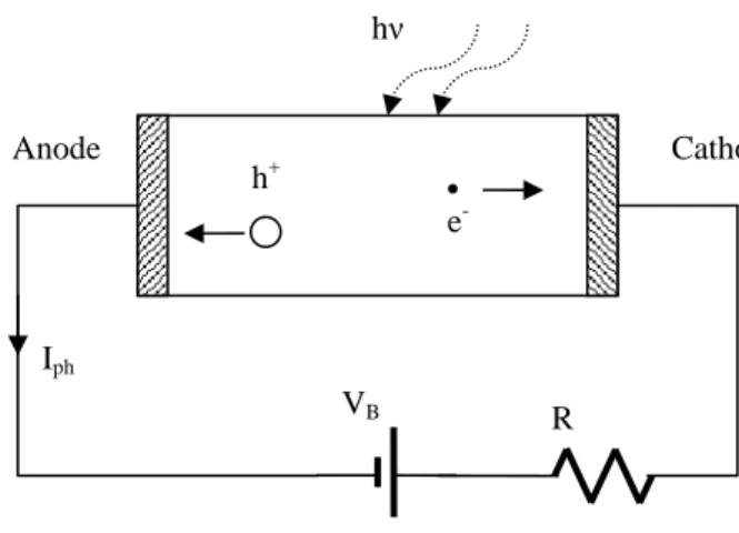
Photodiodes currently are the most frequently used photodetectors in industry because of their efficiency and low cost. A standard simple photodiode has semiconductor material and some junctions such as metal-semiconductor (Schottky), p-n, and p-i-n. The main mechanism is the following; when photons that have energy (hν) that is higher than the band gap of the semiconductor (EG) incident up on the junction are absorbed. They produce electron-hole pairs in the depletion region. If a sufficient electric field is applied (in this case if there is a bias) through the depletion region, the charged carriers then produce a measurable electric current (Iph). Therefore, it is required that a photodiode must be reversely biased (VB) in order to work. Figure 2.1 schematically explains the operation of a simple diode [22-23].
hν Anode Cathode h+ e -Iph VB R
Figure 2.1: Schematic diagram of a simple photodiode operation.
2.2 The Schottky Junction
The Schottky junction (also known as a metal-semiconductor junction) is made up of a metal and a semiconductor material. The name was taken from
Walter H. Schottky who explained the rectifying behavior of this type of contact
in 1930.
Making a Schottky contact (junction) is relatively easy. Depositing a metal on a semiconductor is sufficient to create them. Unfortunately, it is not possible to make a perfect Schottky barrier contact with just any metal placed on a certain semiconductor. Some metals tend to diffuse into the semiconductor. Eventually, the rectifying behavior of the contact disappears.
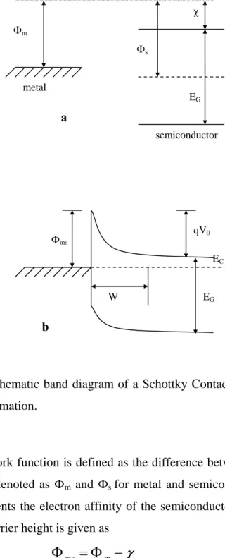
When a metal is deposited on a semiconductor, a phenomenon called Fermi Level Pinning occurs. [24] That is, in thermal equilibrium, the Fermi levels of each material should be equal. The band diagram of a Schottky contact is shown in figure 2.2.
CHAPTER 2. THEORY 7
Vacuum level
Figure 2.2: Schematic band diagram of a Schottky Contact. (a) before (b) after the contact formation.
The work function is defined as the difference between the vacuum and Fermi levels denoted as Фm and Фs for metal and semiconductor, respectively. Here χ represents the electron affinity of the semiconductor. Then, for an ideal contact the barrier height is given as
χ
−
Φ
=
Φ
ms m (2.1)Additionally, the contact potential qV0 is given as
)
(
0 ms
E
CE
FqV
=
Φ
−
−
(2.2)Using the abrupt junction approximation, we conclude that the depletion layer width is given as [23], EG W EF Фms χ Фm EC Фs EF metal EG a EV semiconductor qV0 EC b
⎟⎟
⎠
⎞
⎜⎜
⎝
⎛
−
−
=
q
T
k
V
V
qN
W
B D 02
ε
(2.3)where ε is the dielectric constant and ND is the n-type donor density of the semiconductor. Here, V denotes the applied bias voltage to the junction.
There are four main mechanisms for current transportation in a Schottky barrier, such as thermionic emission, tunneling, recombination/generation in the depletion region, and recombination/generation in a neutral region. The main transport mechanism is the thermionic emission over the barrier also produces the ideal diode characteristics to the junction. Crowell and Sze proposed the expression for the I-V characteristics of a Schottky barrier junction.
⎟⎟
⎠
⎞
⎜⎜
⎝
⎛
−
=
kT1
qV Se
I
I
(2.4) kT q S mse
T
A
I
Φ −=
** 2 (2.5)where A** is the effective Richardson constant.
2.3 The Band-gap of Al
xGa
1-xN
The band gap of AlxGa1-xN with respect to Al concentration x is calculated with the empirical formula
(
x
)
E
bx
(
x
)
xE
E
g=
g,AlN+
1
−
g,GaN−
1
−
(2.6)where b (0<b<1) is the bowing parameter that is measured experimentally. There are a number of values for b reported in the literature [25 and references therein]. In this present work we used b = 0.62 eV.
2.4 Metal-Semiconductor-Metal Photodiodes
MSM photodiodes are one of the simplest photodetectors in terms of epitaxial growth and fabrication. They are formed by two back to back Schottky
CHAPTER 2. THEORY 9
junctions on a semiconductor surface. When a bias is applied, one of the junctions becomes reversed and the other one becomes forward. Since it is a unipolar device one of the junctions will always be reverse biased. Therefore, current is not allowed to pass in each direction. [3]
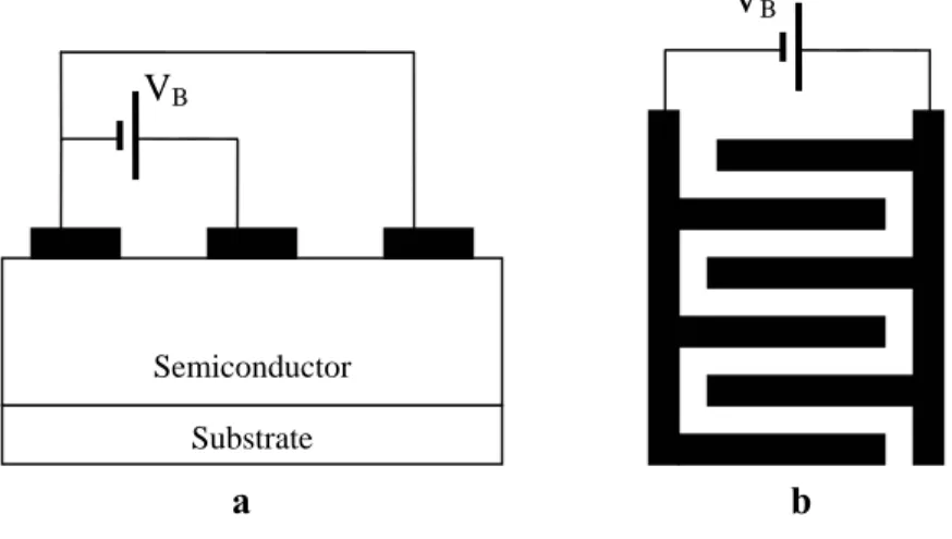
VB
Figure 2.3: Schematic views of an MSM photodetector. (a) cross-sectional view (b) top view.
There is a certain limit for the electric field that can be applied through the semiconductor. Moreover, depleting the carriers between the electrodes is important. Therefore, high bias voltages sometimes are required for the depletion of the entire area. In order to overcome these issues and efficiently collect the incident radiation, the metal electrodes are often interdigitated (see figure 2.3). Interdigitated fingers also reduce the carrier transit time, and therefore, the speed of the device increases.
MSM photodiodes are very easy to realize, especially in materials such as AlGaN/GaN. Due to growth complexities, it is rather difficult to grow complex epitaxial structures. Contrarily, MSM devices only require a single epitaxial layer. Moreover, the fabrication of these kinds of devices is
Substrate VB
Semiconductor
straightforward. They are compatible with integrated circuit processing and are suitable for high speed applications. Although these rather nice properties exist, there is another issue about the basic properties of metals. Metals are very good reflectors of electromagnetic radiation. In addition, the skin depth values for metals are rather low (~15-20 nm). Therefore, in MSM structures, nearly half of the light can go through the semiconductor. There are two possible solutions to this problem. The first one is to make the electrodes as thin as possible so they can transmit as much light as possible. This is also the method we used in this present work. The other method is the back illumination of the device. However, in this case your substrate and underlying layers should also be transparent to the incident radiation.
2.5 Photodetector Characterization
Commonly defined figures of merit exist for detector characterization. These are current voltage, quantum efficiency and responsivity, noise and detectivity, and time response characteristics [8, 22-24]. Here we will discuss current voltage, quantum efficiency and responsivity and noise and detectivity characteristics which were carried out in this present work.
2.5.1 Current-Voltage Characterization
The main current-voltage behavior of a diode depends on the type of junction used. Although MSM structures have a Schottky junction inside, we cannot see the real Schottky behavior in the I-V curve. What we can see is just the reverse bias characteristics. Equation 2.4 represents the ideal forward current voltage relation of a Schottky junction. However, there is a correction to that equation as
⎟⎟
⎠
⎞
⎜⎜
⎝
⎛
−
=
nkT1
qV Se
I
I
(2.7)CHAPTER 2. THEORY 11
where n is the ideality factor (n≥1). If n = 1, this means that we only have a thermionic emission. Otherwise, the other carrier transport mechanisms are involved.
IS in the equation is ideally the reverse saturation current of the diode. The MSM structures equation 2.5 is insufficient to explain the reverse current characteristics. We have to include the hole components as well, because there are two diodes and one of them is in forward bias. The overall expression for dark current is therefore
kT q p kT q n p ms n ms
e
T
A
e
T
A
I
=
* 2 − Φ+
* 2 − Φ (2.8)where An* and Ap* are effective Richardson constants for electrons and holes, respectively. Фms values also differ for the different carrier types.
2.5.2 Responsivity and Quantum Efficiency
The quantum efficiency of a photodetector is defined as the probability of generating an electron-hole pair that will contribute to the photocurrent by way of a single photon. It is a wavelength dependent quantity and is expressed conventionally as
)
1
)(
1
(
)
(
λ
R
e
α(λ)dη
=
−
−
− (2.9)where R is the reflectivity of the top surface, α(λ) is the absorption coefficient and d is the absorptive layer thickness. Efficiency increases with an increasing absorption layer thickness. However, thick layers cause longer carrier transit times. Therefore, the detector is slower. This phenomenon is called the efficiency-bandwidth trade off. Furthermore, efficiency drops rapidly when λ becomes larger than the corresponding band gap wavelength.
Responsivity is another measure to characterize a photodetector. It is defined as the outcome produced (current or voltage) per incident optical power.
Therefore, it usually has the units A/W or V/W. The responsivity is related to the quantum efficiency as
1240
)
(
)
(
nm
h
e
P
I
R
phη
λ
υ
η
λ
=
=
=
(2.10)2.5.3 Noise and Detectivity
The current generated by a photodiode is not always due to an optical source. There are other effects that produce random currents, mainly noise.[22] There are three sources of noise mainly. The first one is Shot noise and is due to the random generation of carriers across the potential barriers. The frequency dependent Shot noise current is given as
f
I
q
f
i
s2(
)
= 2
∆
(2.11)where <I> is the dark current and ∆f is the bandwidth. The second important noise is the thermal (Johnson) noise. It is mainly from the random thermal movements of the carriers and is given as
R
f
T
k
i
t2= 4
B∆
(2.12)where R is the differential resistance. The final and most dominant noise in our detectors is the 1/f (flicker) noise, which is related to trap centers in both bulk or surface and leakage currents. The 1/f noise is defined as
f
f
I
k
i
2f=
B∆
1 (2.13)CHAPTER 2. THEORY 13
As one can see from the above expressions, at high frequencies and high bandwidths, shot noise is dominant but at low frequencies, 1/f noise becomes dominant.
There is another quantity called noise equivalent power (NEP) and is defined as the minimum optical power required for producing a photocurrent that will give unity in the signal to noise ratio. NEP is given by
R I NEP= n
(2.14)
In is the total noise (i.e. the root mean square of the sum of the three noises provided above), in which R is the responsivity.
Generally, NEP is a small quantity and the smaller the NEP the better the detector. Therefore, another quantity called Detectivity is defined as the inverse of the NEP. More specifically, the detectivity per area is called specific detectivity (D*) and is also defined as
NEP f A D* = ∆
(2.15)
where a is the device active area. The unit of the D* is cmHz1/2/W. There is also another way to calculate D*, [26] which is called a thermally limited detectivity formula, 2 1 0 * 4 ⎟⎠ ⎞ ⎜ ⎝ ⎛ = kT A R R D λ (2.16)
where A is the device area, Rλ is the device responsivity, and R0 is the differential resistance at a corresponding voltage. Rλ and R0 are measured at a 0 V bias.
Chapter 3
Design and Growth
In this chapter, we first provide the fundamental MOCVD background. Topics such as what are the basic parts and basic operation will be covered. Then, we will move on to the design of our wafers. Finally, we explain in detail the growth process of our wafers.
3.1 Metal-Organic Chemical Vapor Deposition
(MOCVD)
Crystal growth is one of the key aspects for the realization of any semiconductor device. It is important to grow high quality and crack free heterostructures with different layers of materials and specific doping concentrations as well as the growth of high quality single layer crystals in order to make high performance electronic devices [27]. The first successful demonstration of III-V compound growth using metalorganic precursors and hydride sources was reported in 1960 by Didchenco et al. Later, the technique was improved and given the name MOCVD (Metal Organic Chemical Vapor Deposition), also called MOVPE
CHAPTER 3. DESIGN AND GROWTH 15
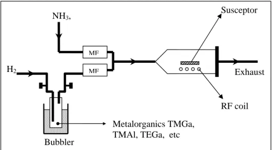
(Metal Organic vapor phase epitaxy). Before that, MBE (Molecular Beam Epitaxy), VPE (Vapor Phase Epitaxy), and LPE (Liquid Phase Epitaxy) were used. Metal Organic Chemical Vapor Deposition (MOCVD) is one of the two key enabling technologies that is critical for growing the heterostructures of III-V compounds (MBE is the other). MOCVD relies on metal-organic compounds, such as trimethyl gallium or trimethyl aluminum, which acts as a precursor for the material in thin films. The materials that are grown contain some combinations of gallium, indium, aluminum, nitrogen, phosphorus, or arsenic. The process consists of transporting the precursors via a carrier gas (in our case H2) to a hot zone within a growth chamber. These precursors either dissociate or react with another compound to produce thin films consisting of a single element or compound. Varying the composition of the deposited materials, and doping in the epilayers, produces the end structure.
Figure 3.1: Schematic diagram of our MOCVD reactor.
The MOCVD system, in which we grow our samples, is located at the Bilkent Nanotechnology Research Center and is an AIXTRON RF200/4 RF-S GaN/AlGaN horizontal flow low pressure MOCVD system. It is composed of three main parts; the Gas Mixing Cabinet (GMC), Reactor Cabinet (RC), and
E-Bubbler MF MF NH3, Susceptor H2 Exhaust RF coil Metalorganics TMGa,
Rack. In addition to these, we have a hydride source NH3, SiH4 as an n type dopand, and metalorganic sources such as trimethylgallium (TMGa), trimethylaluminum (TMAl), triethylgallium (TEGa) for III sources, and bis-cyclopentadienylmagnesium (Cp2Mg) as a p type dopand.
GMC is where we arrange all the required combinations of gas mixtures that we sent previously to the reactor. The epitaxial films are produced according to the concentration of each individual molecule in this mixture. GMC consists of many electronically controlled mass flow controllers and pneumatic three way valves, which are used to adjust the gas mixture concentration. RC is where the reaction and deposition occur. It consists of a vacuum chamber, radiofrequency (RF) coil, rotary pump, antechamber, and susceptor. Using an RF generator, we control the temperature of the susceptor, and therefore, the reaction. We can heat the susceptor up to 1,200°C. The pump helps us to regulate the pressure inside the reactor. The antechamber is for loading and unloading the wafers. The susceptor is the part where we place our wafers. Finally, the E-Rack is the component that has all the electronic control units. It is controlled by a computer with which we write the relevant recipes and control the reaction.
3.2 Material Design and Growth
3.2.1 Al
0.75Ga
0.25N Design
An AlxGa1-xN material system exhibits a band gap from 3.6 to 6.2 eV with increasing x. This corresponds to a wavelength interval between 200 and 360 nm. In order to make a photodetector sensitive in the deep-UV region we need to grow AlGaN templates with a very high Al concentration. It is very difficult to grow high quality, crack free even single layer templates with this much Al concentration. Rather little research has been conducted by other groups on this high of an Al concentration in the AlGaN layers that were reported in the
CHAPTER 3. DESIGN AND GROWTH 17
literature [19-20]. Our aim was to construct a simple MSM photodetector, and therefore, we do not need any complex heterostructures other than a single layer high quality AlGaN layer.
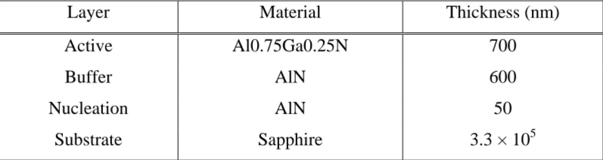
There is a ~10% lattice mismatch between sapphire and AlGaN. Because of that, an AlGaN epitaxial layer cannot be grown directly on sapphire substrate. Even if we manage to avoid cracks, many dislocations that will act as trap centers for carriers will in turn increase an unintentional doping concentration, which will increase the leakage current. Therefore, it is customary to introduce mid layers such as a nucleation and buffer layer between the substrate and epitaxial layers. You can see our epitaxial design shown in table 3.1. These additional layers reduce the horizontal strain due to the lattice mismatch, and increase the crystal quality of the top layer.
Layer Material Thickness (nm)
Active Al0.75Ga0.25N 700
Buffer AlN 600
Nucleation AlN 50
Substrate Sapphire 3.3 × 10⁵
Table 3.1: Epitaxial design of the Al0.75Ga0.25N wafer.
3.2.2 Al
0.75Ga
0.25N Growth
A high quality Al0.75Ga0.25N epitaxial layer was grown in an MOCVD system located at Bilkent University on double sided polished c-plane sapphire substrate. These sapphire substrates are commercially available from a number of companies throughout the world. Prior to the growth, we increased the wafer temperature to 1,100°C and decreased the pressure to 10 mbar for desorption for 10 minutes. During the desorption, any undesired materials deposited, such as dirt on the sapphire substrate, evaporates and washes out by way of H2 purging gas. This step is mainly aimed at cleaning and preparing the sapphire substrate
for growth. The H2 purging flow rate was maintained at 8500 sccm during this step. After desorption, the reactor was cooled to 840°C to grow a thin (~50 nm) AlN nucleation layer. H2 was used as a carrier gas throughout the entire growth process. The TMAl and NH3 flow rates were 20 sccm and 1000 sccm, respectively. At this temperature, Al and N atoms grew as an amorphous layer on the sapphire. Afterward, we heated up the rector at approx. 1,150°C for 10 minutes in order to make that amorphous layer a single crystal layer. Since the layer is rather thin; Al and N atoms can easily align themselves as a wurtzite structure. The nucleation layer helps to overcome the lattice mismatch problem of the AlGaN material system and sapphire substrate. After the growth of the nucleation layer a 700 nm high temperature AlN buffer layer was grown at approx. 1,140°C. The flow rates of TMAl and NH3 were adjusted to 40 sccm and 150 sccm, respectively. This buffer layer reduces the strain effects as we grow away from the sapphire. Finally, we grew an unintentionally doped 600 nm thick Al0.75Ga0.25N active layer. The growth conditions were as follows. The reactor temperature was set to 800°C and the flow rates were 15 sccm, 5 sccm, and 300 sccm for TMAl, TMGa, and NH3, respectively. When the growth of the active layer was finished, we started cooling the reactor to room temperature. While cooling, we kept the NH3 flow on the surface of the wafer. This ammonia flow helps prevent crack formation, and in a way also polishes the surface of the wafer.
To check the Al concentration of our wafer we performed a spectral transmission measurement. We know that sapphire is transparent in the UV range and the band gap of AlN is 6.2 eV, which corresponds to an absorption edge of approx. 200 nm. Therefore, we can see the absorption edge of the Al0.75Ga0.25N layer exactly with the spectral transmission measurements. Using equation 2.6 with the measured absorption band edge, and therefore, band gap energy, we can determine the exact concentration of the Al in the active layer.
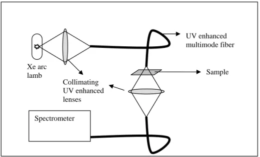
We used an Ocean Optics Chem2000-UV-VIS PC Plug-in Fiber Optic Spectophotometer for the spectral transmission/reflection setup, a schematic of
CHAPTER 3. DESIGN AND GROWTH 19
which is shown in figure 3.2. We have an Xe arc lamp for the UV source. We collimated the output of the lamp by a UV enhanced collimating lens to a multimode UV enhanced fiber by which we illuminated our sample. We have another collimator after the sample, which collects the transmitted light. Finally, we have a spectrometer that consists of a grating and CCD array.
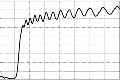
Figure 3.3 shows the performed spectral transmission measurement of our wafer before the fabrication of the MSM photodetectors. The results indicate a 225 nm sharp cut-off, which corresponds to a band gap of 5.51 eV. Using the equation 2.6 we found an Al concentration of approximately 75%.
Figure 3.2: Schematic diagram of our spectral transmission setup.
As you can see from figure 3.3, for a wavelength larger than the cut-off, we have the Fabry-Perot oscillations that result from the microcavity that is formed by the two epitaxial layers on sapphire. These oscillations are a good sign of the quality of the surface and the bulk itself.
Sample Spectrometer Xe arc lamb Collimating UV enhanced lenses UV enhanced multimode fiber
200 240 280 320 360 20 40 60 80 Transm iss ion ( % ) Wavelength (nm)
Figure 3.3: Spectral transmission measurement of the Al0.75Ga0.25N wafer.
3.2.3 SI- and UD-GaN wafer design
In order to overcome the relatively high leakage problem in GaN over AlGaN templates there has been a number of studies conducted, such as the introduction of a thin AlGaN cap layer deposition on the GaN active layer. This method, however, again suffers from the polarization effects due to the interface between the GaN and AlGaN layers. Therefore, it may not be easy to establish good Schottky contacts on that kind of structure.
We introduced the method that is used in high electron mobility transistors on GaN. This method introduces a semi-insulating GaN buffer layer such that the source-drain leakage is minimized.
Semi-insulating indicates the high crystal quality of the template, which means that we have fewer dislocations in the epitaxial layer, which corresponds to higher resistivity values. The detectivity of a photodetector is directly proportional to the square root of the differential resistance. (See equation 2.16).
CHAPTER 3. DESIGN AND GROWTH 21
Hence, if the resistivity is high, then the detectivity will also be high. One other point is that the leakage current (sometimes called dark current) is lowered when the resistivity is high. It is crucial that the leakage current is very low in order to identify the signal coming from a very weak source. With the intention of high performance such as in single photon detection, leakage current must be much lower than the photocurrent, which can be generated by a single photon.
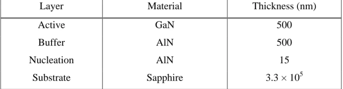
To achieve a better quality GaN crystal, we introduced an AlN buffer layer under the GaN active layer. When growing regular GaN on sapphire we must introduce a nucleation layer in order to overcome a nearly 16 percent lattice mismatch. However, yet again this nucleation layer is insufficient to grow superior quality crystals. Lattice mismatch between GaN and AlN is somewhat easy to handle (about 3 percent). Therefore, using an AlN as a buffer layer might improve the quality of the GaN crystal. We also grew a regular unintentionally doped GaN again on another sapphire substrate for comparison. (See tables 3.2 and 3.3)
Layer Material Thickness (nm)
Active GaN 500
Buffer AlN 500
Nucleation AlN 15
Substrate Sapphire 3.3 × 10⁵
Table 3.2: Epitaxial design of the semi-insulating GaN wafer.
Layer Material Thickness (nm)
Active GaN 500
Nucleation GaN 50
Substrate Sapphire 3.3 × 10⁵
3.2.4 SI- and UD-GaN Wafer Growth
The samples in this study were all grown again on c-face (0001) sapphire substrates by low-pressure MOCVD. Hydrogen was again used as the carrier gas, in which TMGa, TMAl, and NH3 were used as the Ga, Al, and N sources, respectively. An SI-GaN layer was grown on high temperature AlN buffer. Prior to the epitaxial growth, sapphire substrates were annealed for desorption at 1,100ºC for 10 min to remove surface contamination (the details of which were discussed in previous chapters). We started our growth process with a 15nm-thick AlN nucleation layer. To do that, we adjusted the temperature to 840°C. Then, the flow rates of TMAl and NH3 were set to 15 sccm and 300 sccm, respectively. Thereafter, the reactor temperature was ramped to 1,150°C in order to make the amorphous material crystalline. The next step was the AlN buffer layer. Basically, we continued to grow AlN as in the nucleation layer but at not the same temperature. During the growth of these two processes the reactor pressure was 200 mbar. Subsequently, we had a two minute growth interruption in order to reach the optimum growth conditions for GaN. The growth conditions of GaN were as follows: reactor pressure 200 mbar, growth temperature 1,070ºC, growth rate at an approx. 2µm/h of the flow rate of TMGa 15 sccm and the flow rate of NH3 were ramped from 200 sccm to 1300 sccm during the growth. We finished the growth as described previously.
A typical UD-GaN control sample was also grown on sapphire substrate. We used the two-step method. First a 50 nm low temperature GaN nucleation layer was deposited at 500°C. Then, the reactor temperature was ramped up to 1,070ºC. After that, a 500 nm GaN layer was grown. For a fair comparison, the thickness and growth parameters of the high temperature GaN (HT-GaN) layer were selected in the same way as in the previous growth.
We performed a series of measurements in order to compare these two GaN wafers. Two different types of measurements were utilized for the x-ray diffraction (XRD) and photoluminescence (PL) measurements. Both of these
CHAPTER 3. DESIGN AND GROWTH 23
experiments were proof for the grown GaN crystal, in which they provided the information that was related to the crystal quality of our wafers.
XRD measurements were performed in the Semiconductor Technologies Advanced Research Laboratory, Gazi University, Ankara. Since our claim was that the SI-GaN crystal is a better crystal in terms of quality than the UD-GaN crystal, we expected that SI-GaN would result in a narrower XRD peak.
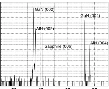
Figure 3.4 and 3.5 demonstrate the XRD ω/2θ scan measurement results. You can clearly see GaN and AlN peaks on each relevant figure. We plotted the experimental data of the GaN peak in one figure (figure 3.6) in order to see the improvement. As you can see in figure 3.6 we obtained a rather good enhancement in terms of crystal quality. The UD-GaN, which was grown using the standard two step method, had a FWHM as 199 arcsec, whereas the SI-GaN sample had a FWHM of 118 arcsec. These measurements were clearly a sign proving the better quality of the SI-GaN.
20 40 60 80 101 102 103 104 105 AlN (004) GaN (004) Sapphire (006) AlN (002) GaN (002) Int e nsit y (a.u) ω/2θ (o)
20 40 60 80 101 102 103 104 105 GaN (004) Sapphire (006) GaN (002) In tensity (a.u ) ω/2θ (o)
Figure 3.5: XRD ω/2θ scan of UD-GaN control sample.
16.8 17.0 17.2 17.4 17.6 0.0 0.2 0.4 0.6 0.8 1.0 Normalized inte ns ity ω (0) UD-GaN SI-GaN
CHAPTER 3. DESIGN AND GROWTH 25
We also performed a PL measurement on both samples. Figure 3.7 shows our experimental setup. We concluded from the following figures (figure 3.8 and 3.9) that we obtained no other crystal or quantum structure that had a band transition energy that was lower than GaN. We could not see the peak of AlN in SI-GaN because the wavelength of our laser is 325 nm, which has energy that is well below the bulk transition energy of AlN. Therefore, we expected no detectivity form our devices above 360 nm.
We also compared the two PL curves of the two samples in a more detailed semilog scale plot (see figure 3.10). As you can see, both of the samples exhibited good results in terms of PL. The FWHM values are 4 nm and 6 nm with the peak wavelengths of 361 nm and 362 nm for SI-GaN and UD-GaN, respectively.
Both XRD and PL measurements are proof enough that we achieved good quality GaN crystals even for UD-GaN, which was grown using the standard two step method. On the other hand, our SI-GaN showed signs of better quality than UD-GaN in terms of these measurements.
Reflecting optics He-Cd laser monochromator Sample CCD camera Collimating optics
350 400 450 500 550 600 650 700 0 1x10⁴ 2x10⁴ 3x10⁴ 4x10⁴ 5x10⁴ PL ( C oun ts ) Wavelength (nm)
Figure 3.8: PL measurement of the SI-GaN sample.
350 400 450 500 550 600 650 700 0 1x10⁴ 2x10⁴ 3x10⁴ 4x10⁴ 5x10⁴ PL (Cou nts) Wavelength (nm)
CHAPTER 3. DESIGN AND GROWTH 27 340 350 360 370 380 390 400 410 420 101 102 103 104 PL (counts) Wavelength (nm) SI-GaN UD-GaN
Chapter 4
Fabrication
The fabrication of any microelectronic device such as our photodetectors requires a number of sequential steps. The final electrical and optical performance of the device is extremely dependent on these successive steps. Generally, these steps include ohmic/Schottky contact deposition, passivation, etching, air bridge formation, and double Bragg mirror (DBR) deposition. Unfortunately, these steps are not standard for all material systems. Each material requires its own fabrication technique. Fortunately, Metal-Semiconductor-Metal (MSM) devices have no complex fabrication steps such as DBR deposition and air bridges.
Our fabrication process consists of a standard microwave compatible with four steps adopted for an AlxGa1-xN material system. [26,28] This chapter represents these four steps in the order of fabrication. All the fabrication steps were performed in a Class-100 Clean Room at the Advanced Research Laboratory at Bilkent University.
4.1 Process Basics
In this part of the thesis, we review the basic process steps of semiconductor device fabrication that relates to our process.
CHAPTER 4. FABRICATION 29
4.1.1 Sample Preparation
Our MOCVD reactor can grow AlGaN material on 2-inch sapphire substrate. It is not possible to perform fabrication on this large wafer as this would result in excessive wasting of the sample. Therefore, it is mandatory to cleave the sample in smaller pieces prior to the fabrication. Typically, one step in our photomask is approx. 6 mm × 6 mm. For that reason, we cut the wafers at approx. 7 mm × 7 mm using a diamond dicer. We scratched the wafer on the back side with a ruler, and then fractured it by hand.
Subsequent to cleaving, we cleaned the surface of the sample. Usually there are cleaving residues and sometimes some organic dust and photoresist residues on the surface. Removing these contaminants is extremely important because they often make the device either open or short. We have two different cleaning techniques.
The first technique is used if there is not a significant amount of dirt on the sample. We put the sample in acetone for a couple of minutes. Acetone dissociates soft organic residues and it helps to remove the inorganic dirt. While the sample remains in the acetone, we gently sweep the surface with a q-tip if there is no features were previously made on the sample. Then, we put the sample in iso-propilic alcohol to remove the acetone. Finally, we put the sample under the running de-ionized (DI) water to get rid of the iso-propilic alcohol. Then, we dried the sample using a nitrogen gun. We put the sample on a hot plate at 120°C for 2 min for dehydration, when it was that the solvent cleaning was over. Afterward, we examined the sample under an optical microscope if there was any dirt left. If so, we perform this process all over again.
The second technique is used when the sample is very dirty with hard organic residues that cannot be removed by acetone. Note that this method can be used only for bare samples. If there is any deposited metal from beforehand, this method cannot be used. We used the so-called Piranha Etching technique. We prepare a solution of 3:1 H2SO4:H2O2. This is an extremely strong solution
for organic and metallic materials. We put our sample in this solution for 5-10 min (according to the dirt level of the sample). Then, we use DI water to clean the sample. Finally, we again use a hot plate for dehydration at 120°C for 2 min. Typically, one round is enough with this technique for cleaning the surface.
4.1.2 Photolithography
Photolithography is the most important part of the microfabrication processes. Because it is the part in which we define the features on the sample. Thus, it is required in every step. We use a polymer called photoresist, which is sensitive to UV light. By exposing with UV over a photomask we transfer the patterns on the mask to the photoresist. Then, etching and material deposition can be performed on the patterned photoresist.
We use AZ5214E image reversal photoresist, which is sensitive to 360 nm UV light and capable of patterning feature sizes ~0.7 µm. It can also be used as positive photoresist and is etch resistant. AZ400K developer is used to remove exposed parts of the photoresist. We utilize the Karl Suzz MJB3 Mask aligner for positioning and aligning the mask.
Thereafter, the cleaning hexametyldisilazane (HMDS) is coated on the surface in a spin coater. Then, the photoresist coating is performed. The thickness of the photoresist is related to the speed of the spinner. Every step requires its own photoresist thickness. If we aim too small, features such as 1 µm, we then need thin resist. If we perform deep dry etching, then it is better to coat with thicker photoresist. Typically, we spin our photoresist at 5,000 rpm for 40 s, which corresponds to a photoresist thickness of 1.3 µm. If we are performing mesa isolation etching, then we use 3,000-3,500 rpm for 40 s, which corresponds to a photoresist thickness of ~1.6 µm. After the spin, the samples are pre-baked at 110°C for 55 s.
There are two types of lithography such as positive and image reversal photolithography. The basic difference in these two is that in positive lithography the features on the mask are transferred in the same way to the
CHAPTER 4. FABRICATION 31
sample. That is, the closed (dark) features in the mask will be transferred, whereas in image reversal lithography, the patterns on the sample are reversed. That is, the open features in the mask will be transferred to the sample.
4.1.2.1 Positive Photolithography
In this method photoresist coated and pre-baked samples are exposed with an Hg lamp in the mask aligner after the alignment for approx. 40 s at 4 mW/cm2, which makes 160 mJ/cm2 and is enough to activate the photoresist. It is in this way that we activated the photoresist directly. Then, the samples are developed with 1:4 (AZ400K:H2O) diluted developer for approx. 40 s. This method is used for thin metallization and etching steps.
4.1.2.2 Image Reversal Photolithography
The main difference in this method is that we expose the sample twice. First, we expose the sample for approx. 60 mJ/cm2 with the mask, and then we post-bake the sample at 120°C for 120 s. Finally, we expose the sample again without the mask for 160 mJ/cm2. This step is called the flood exposure. In this method the first exposure defines the features but it is insufficient to activate the photoresist. Then, when we post-bake it, the polymeric structure of the exposed photoresist changes so that after the flood exposure the opaque parts on the mask will be activated. The development part is the same as the previous method. This method is especially designated for thick metallization and small feature sized processes. Because the photoresist in our case is designed for image reversal applications, the resolution is, therefore, higher in this case.
4.1.3 Etching
Etching is one of the basic steps of microfabrication. Since devices generally utilize heteroepitaxial structures, one has to etch in order to reach deeper layers. Fortunately, MSM structures are rather simple structures. We do not have an under layer that we have to make contact with. We require the etcing for two purposes only. One is the separation of the devices from one another and the other is after surface passivation, in which we need to remove
insulators from certain parts in order to make contact. There are two types of etching; dry etching and wet etching.
4.1.3.1 Dry Etching
There are a number of techniques used for dry etching in semiconductor device fabrication technology. Reactive Ion Etching (RIE), plasma etching, Ion milling are examples of dry etching techniques. In our lab, we use a RIE facility that etches the surface by accelerating reactive ion plasma in a low pressure environment. The ions remove the surface atoms by chemical reaction or simply by physical collision. For etching AlGaN and GaN materials we used CCl2F2 gas as an etchant. Etch rates differed from 20 nm/min to 45 nm/min for AlGaN and GaN.
4.1.3.2 Wet Etching
Wet etching was the first etching technique to ever be used in semiconductor science. It is based on chemical reactions between the substrate surface and the etchant solution. When a substrate is put in its etchant solution, the reaction initiates and eventually the substrate is removed from the surface. We use wet etch to etch SiNx which we deposit on top of the surface for passivation. In order to etch SiNx we use 1:100 dilute HF solution. Etch rate is typically 30 nm/s.
4.1.4 Deposition
It is not possible to grow all the layers as needed via epitaxy. One has to deposit additional material such as metals for contacts and dielectrics for electrical isolation or optical components such as mirrors, waveguides etc. In our process, we deposit metals for contacts and SiNx for surface passivation and antireflection coating purposes.
CHAPTER 4. FABRICATION 33
4.1.4.1 Metallization
We deposit metals on the samples for different purposes. In the case of MSM photodiodes, we need two kinds of metallization such as Schottky contact formation and interconnect metallization.
We have an ultra high vacuum (UHV) LE590 box coater for metal depositions. It is a thermal evaporator. Metals are placed in tungsten boats. Then, they are evaporated by running a high electrical current through these tungsten resistors in UHV. The deposited metal thickness is monitored throughout the process via detectors. Therefore, we can precisely adjust and monitor the deposited metal thickness.
4.1.4.2 Dielectric Coating
All the dielectric coating steps are performed in a Plasma Enhanced Chemical Vapor Deposition (PECVD) system in our laboratory. The system uses different gases as the reaction precursors. For SiNx coating, we use silane (2% SiH4+98% N2) as the Si source and ammonia (NH3) as the N source. We have a vacuum chamber in which we create plasma of silane and an ammonia mixture. The flow rates of each gas are crucial for the composition of the deposited material. The ions of plasma are accelerated towards the sample surface, which is heated to 250°C. Then, the reaction occurs. Si and N atoms are deposited as SiNx and the rest is taken out through exhaust.
4.2 Device Fabrication Steps
We fabricated our devices using microwave compatible four steps. These steps are mesa isolation, Schottky contact formation, dielectric coating, and interconnect metallization.
4.2.1 Mesa Isolation
The mesa isolation step is, in essence, the removal of the connection between the devices. By this step the device active areas were defined, and were
isolated form one another. Unfortunately, AlGaN material is one of the hardest materials. The etch rate is extremely low and moreover it is comparable to the etch rate of the photoresist. Therefore, this step causes many problems during the process. Generally, mesa isolation is one of the last steps with other materials. We on the other hand changed the sequence and started the process with mesa isolation. We generally perform this step twice because photoresist is insufficiently strong to hold all the way down to the sapphire. After this step, there are semiconductor islands left only on sapphire. (See figure 4.1)
Mesa islands AlxGa1-xN
sapphire sapphire
a b
Figure 4.1: Sample before (a) and after (b) mesa isolation step.
4.2.2 Schottky Contact Formation
This is the most important part of our process because all the physics occurred under these contacts. According to our device geometry, these Schottky contacts are in the form of two separate interdigitated fingers. Because of that, this step is also called finger metallization. The finger width and pitch are in the range of 1 µm to 20 µm. We used Ni and Au for finger metallization. The coated metal thicknesses were 3 nm for Ni and 6 nm for Au. As you can observe, we coat very thin metal in this step. This is because we want our metal to be as transparent to UV light as possible. Normally half of the surface was covered with metal already. Therefore, if we coat with thick metal, then only half of the incident light will be able to enter the device. We deposit thin metal to avoid that situation. (See figure 4.2)
CHAPTER 4. FABRICATION 35
Schottky Metal
sapphire
Figure 4.2: Schottky metallization
4.2.3 Dielectric Coating
This step produces a protective layer on top for finger metals from outside effects as well as it serves as an antireflection layer. We determined the thickness of the SiNx layer as follows. The layer thickness should be λ/2n in order to minimize the reflection for a specific wavelength λ, where n is the refractive index of silicon nitride. We used PECVD to coat the dielectric on the sample. PECVD coats the surface to where the walls of the mesa island are also coated along with the top surface. (See figure 4.3) This property helps us to prevent interconnect metals from touching the semiconductor material. After the deposition, we etch the required parts of the SiNx layer through the openings of photoresist with an HF:H2O (1:100) solution.
a
Dielectric
Figure 4.3: (a) Sample surface after dielectric coating, (b) Sample surface after wet etching with HF.
sapphire
b sapphire
4.2.4 Interconnect Metallization
This is the final step of the device fabrication. The Schottky metal area is very small, and the metal is very delicate. Therefore, we need to make larger and thicker contact pads to be able to test our devices. Interconnect pads have main contacts that are used to touching the two separate Schottky metals. In addition, there are two microwave compatible transmission lines surrounding the device. We again, thermally evaporated the metal for this step as 50 nm Ti and 700 nm Au. Notice that this is a very thick metal, and therefore, we used image reversal photolithography in this step. The main role of Ti here is to make the gold stick to the sapphire surface. See (figure 4.4)
Interconnect metals
sapphire
Figure 4.4: Finalized device.
4.2.5 Lift Off
All the steps involving metallization has a process called lift off. It is the part in which we get rid of the excess metal part coated during thermal evaporation. We placed the sample in acetone. Acetone dissolves photoresist immediately and the metal on the photoresist is lifted off. Sometimes some light agitation is enough for the lift off of the metal, especially in the finger metallization step because the metal is very thin. However, the steps such as in interconnect metallization require more vigorous methods such as ultrasound or even sweeping the sample with a Q-tip.
CHAPTER 4. FABRICATION 37
Step Parameters Mesa isolation etch Photolithography: positive
Spin: 3500 rpm Etchant: CCl2F2
Pressure: 8 mbar Gas flow: 20 sccm RF power: 100 W Finger metallization Photolithography: positive
Spin: 6000 Metals: Ni/Au Thickness: 3 nm/6 nm Silicon nitride deposition Silane flow: 180 sccm
Ammonia flow: 45 sccm RF power: 20 W Pressure: 1000 mTorr Temp: 250°C Thickness: 250 nm Silicon Nitride Etch Photolithography: positive
Spin: 5000
Etchant: 1:100 HF:H2O
Time: ~7 sec. Interconnect Metallization Photolithography: positive
Spin: 5000 Metals: Ti/Au
Thickness: 50 nm/700 nm
After finger metallization
A completed device
Chapter 5
Measurements
This chapter represents our experimental results from the fabricated devices. We fabricated three different wafers. The first detector sample had a low cut-off wavelength and high UV-visible rejection ratio and was fabricated from the Al0.75Ga0.25N wafer. This photodetector is called a Deep-UV photodetector. The second detector sample was fabricated from an SI-GaN sample and its advantage was the lowering of dark current. Finally, the third detector sample was made on a regular UD-GaN wafer, which was used as a reference for comparison with the detector sample two. These two samples are called Visible Blind Photodetectors.
We performed current-voltage (IV), quantum efficiency (QE), responsivity upon low incident optical power and noise measurements on the fabricated devices. We will present these results as two separate chapters. The first chapter will be about detector sample one and the second chapter will be about detector sample two and three.
5.1 Experimental Results of the Deep-UV Photodetectors
5.1.1 Current vs. Voltage Characteristics
Current-Voltage (IV) characteristics were carried out using a Keithley 6517A high resistance electrometer with low noise triaxial cables in a grounded
shielded Faraday cage. Since we were measuring MSM photodiodes, the IV characteristics did not have a diodic character exactly. This is because the structure has two diodes connected back to back so that, normally, the current cannot pass through in each direction. The resulting devices exhibited extremely low dark currents and very high breakdown voltages. Figure 5.1 shows the I-V curve of a 4 µm finger width/spacing device. As you can see, the dark current level is below 100 fA up to ±100V bias voltage (see figure 5.2). This dark current value corresponds to 5.8 × 10⁻¹⁰ A/cm2 dark current density under 50 V bias given the device area of 100 × 100 µm2. We increased the bias voltages up to 350 V and even under this high bias voltage level, dark current does not exceed 100 pA. The curve in the figure 5.1 indicates a sign of soft breakdown when the bias voltage approaches 300 V. These low dark current and high breakdown voltage values were good signs of the high quality of our Al0.75Ga0.25N epitaxial layer.
-300 -200 -100 0 100 200 300 -100 -75 -50 -25 0 25 50 75 100 Voltage (V) Cu rrent (p A)
CHAPTER 5. MEASUREMENTS 41 -1501 -100 -50 0 50 100 150 10 100 1000 Current (fA) Voltage (V)
Figure 5.2: IV Characteristics of a 4 µm finger width/spacing and 100 × 100 µm2 area device in a semilog scale.
5.1.2 Quantum efficiency/Responsivity Measurements
The spectral responsivity measurements were performed in a range of 200 – 400 nm using an Xe lamp, a monochromator, and a calibrated Si photodetector. We recorded the photocurrent using a Keithley 6517A electrometer. You can see the experimental setup in figure 5.3. The continuous output of the Xe lamp passes through a computer controlled monochromator to produce a single wavelength output. The output of the monochromator is sent to the photodetector by a fiber and a fiber micropositioner, which is mounted on the probe station. The electrical connection of our photodetectors is again performed by micropositioners and low noise DC probes. We apply a DC bias with the voltage source of the electrometer and read the current with an ammeter of the electrometer. Prior to the experiment we recorded the optical power output of the Xe lamp and monochromator system with a calibrated Si photodetector. We placed a Si photodetector exactly where we put our own