' · f’ '-*i^f,' -“ ' . '"“'.I ;V‘. ' ' '· · i.-j:*' _.' . ..vr,,^·
CONSTRUCTION OF A SCANNING TUNNELING
MICROSCOPE AND FIRST RESULTS
- » - T H E S I S
S v £ 2 i I i i T T S S T G T H E D B PA £ T M S H T O P P H Y 3 I G S
- ¿ C S T 2 T U T E G P E H G· IN 3 B E I H G- A MB
C F B 2 L I I3' M T Y N IV 3 B * IT V
m '··* ^ ^ --,· — W Jr JT 'T, ■•^i '■’J»· JU t; N·? 4ir JJ 4^ »Ail· Juit li '·■ »4^T /V -j·,. ifHj ,-<
'Tf -^r- ^ Xt W JT*;? '"
2
:» T* 'T'm. u. Jj w *· ^ ■^\ '^ ' Jr C' ,'T« >1^' M· »W «>NV ' ,^’.« ««/ i^.l'^rnci* —P A l i 4 i li i i U 'J J. '*■*'' * . e '· —1
P P n L/ '.v,. * w ,--i. ■.' ' J M '»Mi
^
CONSTRUCTION OF A SCANNING TUNNELING
MICROSCOPE AND FIRST RESULTS
A T H E S I S
S U B M I T T E D T O T H E D E P A R T M E N T O F P H Y S I C S
A N D T H E I N S T I T U T E O F E N G I N E E R I N G A N D S C I E N C E S
O F B I L K E N T U N I V E R S I T Y
I N P A R T I A L F U L F I L L M E N T O F T H E R E Q U I R E M E N T S
FOR THE DEGREE OF M A S T E R O F S C I E N C E
By
Ahmet Oral
January 1990
î^'C.
, S 3 k 0 Í 2 b 3 O j c , \ Ъ · ^ ü ı
Ill
I certify that I have read this thesis and that in opinion it is fully adequate, in scope and in quality, as a thesis for the degree of Master of Science.
^it.% y l A. r C ^
Assoc. Prof. Dr. Recai M. Ellialtioglu (Principal Advisor)
I certify that I have read this thesis and that in my opinion it is fully adequate, in scope and in quality, as a thesis for the degree of Master of Science.
Prof. Dr. Cemal Yalabık
I certify that I have read this thesis and that in my opinion it is fully adequate, in scope and in quality, as a thesis for the degree of Master of Science.
Prof. Dr. Abdullah Atalar
Approved for the Institute of Engineering and Sciences:
Prof. Dr. Mehmet Baray
ABSTRACT
CONSTRUCTION OF A SCANNING TUNNELING
M ICROSCOPE AND FIRST RESULTS
Ahmet Oral
M. S. in Physics
Supervisor: Assoc. Prof. Dr. Recai M. Ellialtioglu
January 1990
In this thesis, construction of a Scanning Tunneling Microscope in air is explained. A step motor sample approach mechanism and a tripod scanner are used in the construction.
Atomic resolution images of graphite samples are obtained in both constant current and constant height modes. Loss of trigonal symmetry in some Graphite images are also observed. This anomaly is attributed to the multiple atom tip or slipped top layer of Graphite.
Keywords: Scanning Tunneling Microscope, Tunneling, Piezo, Scanner, Graphite, Tip.
ÖZET
BİR TAR A M A LI TÜNELLEM E MİKROSKOBU Y A P IM I V E
İLK SONUÇLARI.
Ahmet Oral
Fizik Yüksek Lisans
Tez Yöneticisi: Doç. Dr. Recai M. Ellialtioğlu
Ocak 1990
Bu tezde, atmosferde çalışan, bir Taramalı Tünel Mikroskobu yapımı açıklanmıştır. Tasarımda adım motorlu bir örnek yaklaştırma sistemi ile piezoelektrik tüplerden yapılmış bir üçayak tarama sistemi kullanılmıştır.
Grafit yüzeyinin atomsa! çözünürlükteki görüntüleri değişmez akım ve değişmez yükseklik yöntemleriyle elde edilmiştir. Bazı Grafit yüzeylerinde üçgensel simetrinin kaybolduğu gözlenmiştir. Bu olağandışılık çok atomlu uca yada kaymış üst tabakaya bağlanmıştır.
Anahtar sözcükler: Taramalı Tünel Mikroskobu, Tünelleme, Piezo, Tarama sistemi, Grafit, Uç.
ACKNOWLEDGEMENT
I am grateful to Assoc. Prof. Dr. Recai M. Ellialtioglu for the invaluable guidance, encouragement, and above all, for the enthusiasm which he inspired on me during the study.
I would like to express my deeep gratitude to İsmet Kaya for his collaboration, motivation and his friendly personality.
I would like thank İsmail Doğru, METU Physics Department, for his advices and machining the STM.
I debt special thanks to Prof. Dr. Salim Çıracı, Prof. Dr. Cemal Yalabık and Inst. Erkan Tekman for their encouragement and remarks.
Last but not the least, I wish to thank to Berna Ciner for her helps and continuous moral support.
Contents
A b s t r a c t... iv
Ö z e t ... V A cknow ledgem ent... vi
C o n te n ts...vii
List of Figures x
1 Introduction 1
2 Theory of Scanning Tunneling Microscopy 5
2.1 Transfer Hamiltonian M e t h o d ... 7
2.2
Tersoff-Hamann Theory 9 2.3 Other M e t h o d s ...12
3 Instrumentation 14 3.1 Vibration I s o la t i o n ... 15 3.2 Mechanical Design of S T M ... 18 3.2.1 Coarse Approach U n i t ... 19 v ii3
.2.2
Scanner22
3.2.3 T i p ... 25
3.3 The Control System 28 3.4 Electronics and Computer In te rfa ce ... 33
3.4.1 I -V C on verter...
34
3.4.2 z-Scanner E lectronics...35
3.4.3 x& y Piezo D r i v e r ... 37 3.4.4 Data A c q u is it io n ... 38 3.4.5 Image P r o c e s s in g ... 39 3.4.6 Low Pass F i l t e r ... 39 3.4.7 Median F i l t e r ... 414 Related Techniques and Applications 42 4.1 Atomic Force M icroscop y... 43
4.2 STM L ith ograp h y... 45
4.3 Near-held Optical Scanning M icro sco p e ... 47
4.4 Scanning Tunneling Optical M icroscop e... 48
4.5 Ballistic Electron Emission M ic r o s c o p e ... 49
4.6 Scanning Tunneling P o t e n t io m e tr y ... 50
4.7 Secondary Particle Emission in S T M ... 51
4.8 Scanning Tunneling S p e c tr o s c o p y ... 52
4.9 Detection of Gravity Waves using S T M ... 54
4.10 Scanning Capacitance M ic r o s c o p e ... 55
4.11 Scanning Ion Conductance M ic r o s c o p e ... 55
4.12
Appliccition of STM to Biology and Chemistry 565 Results 58
5.1 E xperim ents... 61
6 Conclusions 66
Bibliography 68
List of Figures
1.1
Schematic diagram of STM ... 31.2
Comparison between microscopy techniques. 42.1
One dimensional potential barrier... 53.1 Schematic diagrarñ of STM ... 15
3.2
Simplified model for Vibration Isolation System. 16 3.3 Transfer function for single stage Vibration Isolation System. 17 3.4 Scanning Tunneling Microscope. 19 3.5 A micrometer screw driven by a step m otor... 203.6 Motor Drive Circuit...
22
3.7 Single Tube Scanner 23 3.8 Scanner Unit ... 25
3.9 Effect of multiple atoms at the apex of the t i p ... 26
3.10 Tip e t c h i n g ... 27
3.12 Block diagram of the Feedback System... 32
3.13 Root-Locus plot of T {s )... 32
3.14 Block diagram of the STM electronics... 34
3.15 I-V converter. 35
3.16 z-scanner electronics. 36
3.17 High Voltage Amplifier. 37
3.18 x -y Scanner Electronics. 38
3.19 The convolution window. 40
3.20 Low Pass Filter performance. 40
3.21 Median Filter Performance. 41
4.1 Atomic Force Microscope. 43
4.2 Some AFM images. 45
4.3 Photon ‘Tunneling’ through the barrier. 48
4.4 Energy levels in ВЕЕМ. 49
4.5 Form of the wavefunctions for various energies. 53
5.1 Structure of the graphite. 59
5.2
Brillouin Zone of the graphite... 605.3 A constant current image of a graphite sample. 62
5.4 Constant height image of a graphite surface... 63
5.5 Another constant height image of a graphite surface. 63
LIST OF FIGURES
5.6 An anomalous image.
x n
Chapter 1
Introduction
The transmission of particles across a classically forbidden region in which the particle can not exist, is called tunneling. The phenomena is purely Quantum Mechanical and is a direct consequence of the wave-particle duality.
Tunneling phenomena has been proposed by Oppenheimer [
1
] in 1928 to explain autoionization of Hydrogen atoms in very high electric fields. Fowler and Nordheim [2
] have explained electron emission from metals under intense electric fields with tunneling to the vacuum, which was observed in 1922.The first experimental observation of tunneling in solids has been achieved by Esaki [3] in 1958. His tunnel diode is one of the most important application of tunneling, which led today novel tunneling devices. In 1960, Giaver [4] has observed superconducting energy gap by using a superconductor-insulator- normal metal junction (SIN) and developed tunneling spectroscopy. In 1962, Josephson [5] has investigated novel features in SIS structures, later called Josephson junctions. Esaki, Giaver and Josephson were awarded with Nobel Prize in Physics in 1973 for their fundamental works on tunneling.
Devices, using tunneling phenomena, such as MIM diodes, hot electron transistors, s q u i d’s were also developed in 70’s. Another application of the
tunneling is Inelastic Electron Tunneling Spectroscopy (lETS) [
6
]. Organic molecules are adsorbed on an oxide surface of a MIM junction, before the lastCHAPTER 1. INTRODUCTION
electrode was formed. If energy of the tunneling electrons coincides with one of the vibrational energy levels of the adsorbate, tunneling electrons interact with the molecule and tunneling current changes. Changes in the tunneling current can be observed if is plotted as a function of voltage. Therefore, vibrational energy levels of the adsorbate can be obtained.
Tunneling experiments are performed with oxide barriers until 80’s. The vacuum, instead of an oxide as a barrier, is very attractive for many reasons. First of all, the barrier width can be changed easily. Bare surface properties are not affected by the oxide layers. However, vacuum tunneling was not achieved due to technical problems, mainly vibration isolation until early 80’s.
Young et al. [7] developed a microscope, called ‘ Topogrofiner’ by using field emission rather than tunneling in 1972. This instrument is very similar to the Scanning Tunneling Microscope. It has a sharp field emission tip scanned over the sample by means of piezoelectric translators. The field emission current is kept constant by adjusting the position of the tip during the scan. The resolution was approximately lOOOA in lateral direction. The topogrofiner can be thought as the ancestor of Scanning Tunneling Microscope.
Binnig, Rohrer and coworkers [
8
] have observed vacuum tunneling on platinum samples with tungsten tip and constructed the Scanning Tunneling Microscope [9] in 1982. In 1986, Binnig and Rohrer were awarded with the Nobel Prize in Physics for their construction of Scanning Tunneling Microscope.Teague [10] and Poppe [11] have observed vacuum tunneling before Binnig and Rohrer. But their interest was not to use it in a microscope.
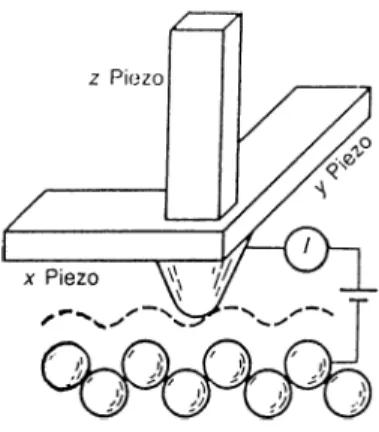
The underlying physical principle of the Scanning Tunneling Microscope (STM) is very simple, the electron tunneling.
A very sharp metallic tip is placed very close to a metal surface to form a vacuum tunnel junction. The tunneling current is a very sensitive function of barrier width. It approximately changes one order of magnitude for lA change in gap width. Therefore, most of the current is concentrated at the apex of the
CHAPTER 1. INTRODUCTION
Figure ,
1
.1
. Schematic diagram of STM.tip. This very fine current filament is scanned over the surface. The z-f)osition of the tip is adjusted with a control circuit to keep the tunnel current constant as shown in Figure
1
.1
.Therefore, z-position of the tip corresponds to constant current contour- plots. If the surface has uniform electronic properties (for example, free electron metals), then these contours corresponds to the topography of the surface. Since tunneling current ?Jso depends on surface densities of states, STM line scans have also information about local electronic proi^erties of the surface. Therefore, it is possible to perform spectroscopy in atomic scale with STM. This method is called Spatially Resolved Spectroscopy or Scanning Tunneling Spectroscopy (STS) and successfully applied to semiconductors and superconductors.
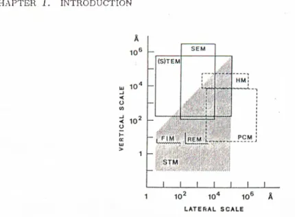
Scanning Tunneling Microscope is a very local probe that can map the surface structures with atomic resolution. Surface structures have been studied by conventional electron microscopy (SEM, ТЕМ , FIM), diffraction measurements ( LEED, X-ray, He diffraction ) and scattering (ion scattering) experiments. Although some of them give atomic resolution in very extreme conditions, direct imaging of surfaces with atomic resolution seemed to be impossible before the invention of STM. Figure
1.2
shows comparison between conventional microscopes and Scanning Tunneling Microscope.Scanning Tunneling Microscope can image only metals or doped semicon ductors. This can be thought as a limitation on the applications. However,
CHAPTER 1. INTRODUCTION
Figure
1
.2
. Comparison between microscopy techniques.Lateral and depth resolution of several microscopes: scanning electron microscope (SEM), (scanning) transmission electron microscope ((S)TE M ), high-resolution optical microscope (HM), field ion microscope (FIM), reflection electron microscope (REM ), phase-contrast
microscope (PCM ) and scanning tunneling microscope (STM ) (after Ref. [9]).
invention of the STM led to the development of wide variety of Scanning Probe Microscopes which will be discussed in Chapter 4. These techniques can be applied to almost any materials (insulators, optical materials, magnetic materials etc.) and open very fascinating opportunities in science and technology. Moreover, applications of the Scanning Tunneling Microscope has a very broad spectrum, extending from biology to chemistry. Development of STM has opened a new era in the surface science.
In this thesis, the construction of a Scanning Tunneling Microscope will be explained. In Chapter
2
, theory of tunneling and Scanning Tunneling Microscope will be given. Instrumentation will be explained in Chapter 3. In Chapter 4, applications of the microscope and related techniques will be reviewed. Results obtained with the microscope will be presented in Chapter 5. Chapter6
concludes the thesis.Theory of Scanning Tunneling
Microscopy
Chapter 2
Different methods have been developed to calculate the tunneling probability through a potential barrier since the birth of Quantum Mechanics.
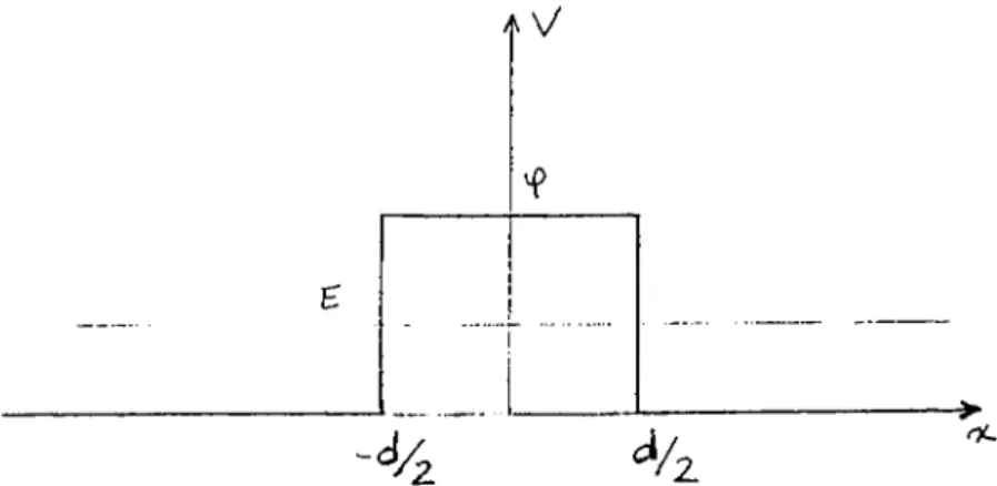
The simplest model to describe tunneling between two systems separated in space is the one dimensional potential barrier. This model is treated in almost every Quantum Mechanics textbook and illustrated in Figure 2.1.
oc
Figure
2
.1
. One dimensional potential barrier.Although it is impossible for a particle to pass through the barrier classically, the particle can tunnel through the barrier with a finite probability. If the barrier is large and wide compared to characteristic quantities, the tunneling probability for a pcirticle from left to right is given by
CHAPTER 2. THEORY OF SCANNING TUNNELING MICROSCOPY
T oc (2.1)
where d is the barrier width, and k = is the inverse decay length of wavefunction in the barrier, (f> and E being the barrier height and incident particle’s energy, respectively.
Although the model is too simple to represent all the features of a tunnel junction, for example the one in STM, it gives the correct form of the tunneling probability as a function of gap distance.
In metals, electrons at the Fermi Level behave like free electrons with an associated effective mass. The work function, (j), is defined as the energy required to move an electron from Fermi level to the vacuum. Therefore One Dimensional Barrier model works quite well for the metai-insulator-metal tunnel junctions.
Simmons [
12
] has calculated the tunneling current density for two metal electrodes asJ = d - e y /
2
) e - ^ V d ^ - ^ ‘^ + + e V l 2 ) e ~ ^ ^ eV/2)d(
2
.2
)where is the average of the metal work functions and c is a constant. This expression is valid even for V > Field Emission regime, and reduces to the following expression for small bias condition, F <C
h iir'^d
2
ko= 1.025\A.
2.1
Transfer Hamiltonian M ethod
Bardeen [13] has developed a general formalism for the theory of tunneling from many particle point of view. Although his theory is one dimensional, it can easily be genercilized to three dimensions. He assumed two many-body systems separated by a barrier extending from a:„ to Xi,. Metal a is at the left of Xa and rnetcil b is at the right of Xb- Then, he considered two many particle states of the whole system, -i/’o and tl>mn· i’ mn differs fx’om ■
0
o in that, only one electron is transferred from the state |m > at a to the state |n > at h.Furthermore, and il}mn are assumed to be the solutions of the Schrödinger Equation in different regions.
CHAPTER
2.
THEORY OF SCANNING TUNNELING MICROSCOPY 7Hißo — Eoi^o fo r X < Xb
EfYiYilpifiji fo r X ^ Xq .
(2.4)
Therefore both wavefunctions are good solutions of the system in the barrier region. The time dependent wavefunction describing the system can be constructed with linear combination of ipo and 'f nm in a very similar way to the time dependent perturbation theory
(2.5)
If we substitute the above ecjuation to the time dependent Schrodinger’s equation
M ( i ) = i A ^
1
(i) (2.6)and carry out the algebra, we can find the time dependent probability amplitudes.
CHAPTER
2.
THEORY OF SCANNING TUNNELING MICROSCOPYSince particles tunnel from state ?/)q to one can assume that a (
0
) ~1
, bmn(O) — 0 and ^ ( 0 ) ~ 0. These approximations give the following differential ec^uation for the probability amplitude,iSimn(i) = < 'f’my.l'H - fiolV’O > C ‘ (2.7)
The above eciuation can be integiTited easily and then the transition amplitude per unit time from state |
7
r > —> \m> is given by,O-TT
- E„) (2 .8)
where Mmn ~ -£'o|V'o> is the transition matrix element. The delta function sifts only the energy conserving transitions. Since all the states ha,ving right energy contribute to the tunneling, the total tunneling current can be calculated as
It =
2
Tre~ T
y~!
~ Eo) (2.9)Therefore we can evaluate the tunneling current, if we calculate the transition matrix Mmn· Since tpo is the eigenstate of the system for x < Xf,, the integrand vanishes. Then, we can write for Mmn
M „ = f r W H - Eo)<Podr
Jb
(
2
.
10
)
We can add tpoiTi — Emn)‘<Pmn to the integrand, because it is zero for the region b. Since we are only allowing energy conserving transitions, the relation simplifies further to
Mmn — ‘4^o'E.‘4^mn)d:T .
(2.11)
CHAPTER 2. THEORY OF SCANNING TUNNELING MICROSCOPY
Mmn = /(^ /’-nV^V’o - ro^lAnn)dr . (2.12)
Integration by parts yields the following result,
M „ ihJmn(T’ l) (2.13)
where Xa < Ti < æt and
2mh (2.14)
This is the familiar current density operator in the Quantum Mechanics. The transition matrix is related to the current density operator evaluated at a-’ i, somewhere inside the barrier.
Bardeen’s formalism is very similar to time dependent perturbation theory, but it uses an overcomplete basis set for the expansion, because i/iq and V’mn «'■re good solutions of Schrodinger’s Equation in the barrier region. The Eqn 2.9 is Fermi Golden Rule type expression for the total tunneling current.
Bardeen’s formalism is quite powerful , because it can be used to calculate tunneling current for any system, for example superconductor-normal metal junctions, tunnel diode, STM etc. On the other hand, calculation of current density operator, Jmni is very difficult for most of the systems and requires further approximations. His theory is the starting point of the most of the tunneling calculations.
2.2
Tersoff-Hamann Theory
The most successful theory of STM was developed by Tersoff and Hamann [14] in 1983. They applied Bardeen’s formalism to STM by modeling the tip with a metal sphere.
CHAPTER 2. THEORY OF SCANNING TUNNELING MICROSCOPY 10
If the statistical factors are included in the Bardeen’s result (Eqn. 2.9), one can write
2
TreI, = - / { K + eV)] X - £ „ ) (2.15)
HU
where f{E ), V, and i/i,, are Fermi-Dirac distribution function, bias voltage, tip and surface states, respectively.
For low bias condition, V ot lOmV", which is a typical value in STM experiments, the expression reduces to
It = 2ve
h HU - Ef) 6 ( E , - Ef) (2.16)
where Ep is the Fermi level for the metals.
Generalization of the Bardeen’s formcilism to three dimensions gives
2
m j ds- (>a;v>/.„ - ■(2.17)
The surface integral must be calculated at the boundary of the barrier.
They expanded the surface wavefunction into a very general form to calculate the matrix elements as
^ X ] a^exp { - ( Â
;2
+ ¡¿|| + G\)z^ exp {«(¿|| + (5) · x } (2.18)where 1 7 * ,^ = V?Vl t and ¿y are surface volume, inverse decay length of the surface wavefunction and surface Bloch wavevector, respectively.
On the other hand, the tip wavefunction is assumed to have asymptotically spherical form
CHAPTER
2.
THEORY OF SCANNING TUNNELING MICROSCOPY 111
g-A;|f’-7=b|n r ... .
V’m = — ctkRekR (2.19)
where R, ro, fit ^.nd Ct are radius of curvature, position of the center, volume of the tip and a normalization constant, respectively.
If these wavefunctions are inserted in Ecp 2.17, the transition matrix can be found as
1
V>.(ro) .
2777-
(
2.20)
The tunneling current is then
I = 32je^<pH^Vt{Ep)e'^>^^ x \i;,{fo)\^6{E, - Ep) (2.21)
where 'Dt(Ep) is density of states at the Fermi level at the tip.
The tunneling conductance, at is
at a p{ro,Ep) (2.22)
where
p (r,E ) = J2\Mf)\'‘ H E , - E ) (2.23)
is density of states at position r and the energy E, for the surface.
Therefore, if the shape of the tip does not change during the experiment and the gap distance is large, the STM contourplots correspond to the charge density corrugation at the Fermi level. They made use of the independent electrode approximation which makes their theory valid for large tip-sample separations.
CHAPTER 2. THEORY OF SCANNING TUNNELING MICROSCOPY 12
TersoiF and Hamann ai^plied their theory to A u(llO ) (1 x
2
) and(1
x 3) reconstructed surfaces. Their results were in very well aggrernent with the experiment.However, their theory is not valid for small tip-sample separations, the spherical tip approximation also causes some artifacts.
2.3
Other M ethods
Garcia ei al. [15] and Stoll et al. [16] have directly solved the Schrödinger equation to calculate the tunnel current. They assumed different periodic model potentials for the tip and the sample. The tip potential period was kept large enough to decouple the neighboring tips. They have found very similar expression for the tunneling current. They have applied their theories to A u(llO ) (1 X 2) reconstructed surface and obtained successful results.
As the tip approaches towards the sample, they start to interact with each other. If the tip is brought very near to the sample, the interaction becomes very strong and must be included in the calculations.
Tunneling probability can not be calculated by Tersoff-Hamann theory, because the electrodes are now very strongly interacting with each other. A new method should be developed.
Tekman [17] introduced the concept of Tip Induced Localized States (TILS), the states that appear between tip and sample for very small tip-sample distances. They modified the Bardeen’s formalism to include the tunneling through the Tip Induced Localized States and calculated the tunneling current at various tip positions for graphite. He found an enhancement in the corrugation amplitude of a factor > 4.
Qiraci [18] et al. have carried out ab initio total energy, force and electronic structure calculations for tip-sample interactions. They have used graphite monolayer and
2
x2
array Aluminum tip atom for their ccilculation. TheyCHAPTER 2. THEORY OF SCANNING TUNNELING MICROSCOPY 13
have found that a dramatic change in the electronic structure at small tip- sample separations. At this regime, local density of states changes drastically and new tunneling matrix elements must be calculated to find the tunneling current.
Chapter 3
Instrumentation
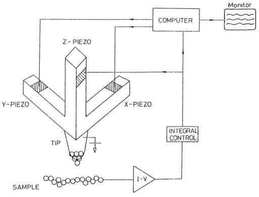
Three dimensional variations in the surface charge density are probed using electron tunneling in Scanning Tunneling Microscopy. Figure 3.1 shows schematic diagram of a Scanning Tunneling Microscope. When a bias voltage is applied between tip and sample, electrons start to tunnel through the vacuum gap, which is typically 10Á. A feedback loop controls the tunnel gap by adjusting the z-position of the tip and maintains a constant tunneling current. The tip is scanned over the surface by x-y piezo translators, change in the z-position of the tip corresponds to the topography of the surface. This configuration is called constant current mode.
The tip can be scanned at constant z-position and variation in the tunneling current resulting from the surface topography can be recorded. This mode is called constant height mode. This mode is faster than the constant current mode, but the surfaces must be smooth to avoid tip crashing.
Important design criteria and instrumentation details are described in this chapter.
CHAPTER 3. INSTRUMENTA'I TON 15
Monitör
Figure 3.1. Sclicmalic diagrain of STM.
3.1
Vibration Isolation
The tunneling current depends exponentiahy on the gap distance variations. This dependence enables us to build a very powerful microscope, the STM. On the other ha.nd, this dependence makes the microscope very sensitive to the external disturbances. Typical corrugation amplitudes measured in constant current mode is of the order of 0.1 Â. Therefore external vibrations coming from the laboratory floor must be damped down to an amplitude of
0.01
 or less. This is one of the most important instrumentation problems we have faced while we were constructing the STM.Vibrations exist mainly at 17,25 and 50 Hz due to motors and transformers that are placed in almost every building. Vibration isolation systems for STM were extensively studied by several authors[19, 20].
CHAPTER 3. INSTRUMENTATION 16
f'igure
3
.2
. Simplified model for Vibration Isolation System.vibrations[
8
]. Later, single or double stage spring s3
'^stems with eddy current damping mechanism were commonly used. In these systems [19], STM is suspended by using metal springs. The vibrations are damped by magnets which induce eddy currents in the metal plates that are placed close to the magnets.Simplified schematic of a single stage vibration isolation system and STM is shown in Figure 3.2.
Vibrations coming from the laboratory floor is transmitted to the STM stage with a transfer function [19]
r -
1 + m / f o Y ‘
1/2
,(
1
- / V Æ P + (2
î/ / / „ )2
, (3.1)where /o is the resonant frequency and ( —
7
/7
C, {'jc = 4iTi7r/o, critical damping coefficient) is the damping ratio of the system. The transfer function is plotted for various (f in Figure 3.3. The resonant frequency should be kept as low as possible to obtain high attenuation. Attenuation is large for small but resonance amplitude is also larger. On the other hand, we can not increase (f very much, because attenuation drops. Therefore we should set ^ to something between 0.1-0.3. Since eddy current damping is usually used, ^ can be adjusted by changing magnets’ position and size.CHAPTER 3. INSTRUMENTATION 17
Figure 3.3. Transfer function for single stcige Vibration Isolation System.
Rubber can also be used instead of metal springs in vibration isolation systems. Four or five stainless steel plates separated by small viton pieces are used for this purpose in Pocket Size STM[
21
]. The viton is used for its Ultra High Vacuum (UHV) compatibilit}^ But these systems have rather low ( >10
Hz) resonant frequency compared to the spring systems.Commercial vibration isolation systems can also be used to support STM. Pneumatic springs are used to suspend a large mass. These systems have usually very low resonant frequency (typically
1
Hz), and adjustable ^ resulting in a very good attenuation.Moreover, the STM has structural damping. The vibrations are dissipated by hysteresis loss due to structural damping of the rigid body. STM can be modeled by a second order system. The transfer function is given by [20]
( f / f .y
[(1
- P / n r + ( / / « A P I · ' “CHAPTER 3. INSTRUMENTATION 18
where fs and Q are resonance frequency and quality factor of the tunnel junction. Therefore rigidly constructed STM, which has high resonance freciuency, does not require vibration isolation[
22
].If f s ^ fo then the transfer function of the whole system is given by[
20
]Ttot = 1 + ( 2 i / / / o ) '
1/2
X ( / / / . ) ■
( { i - P / f i r + U / Q f .r y / ^
. (3.3)
Our system is similar to Pocket Size STM [
21
]. We stacked five brass plates separated by rubber pieces cut from an 0-ring. A marble block , which weighs 70 kg, is placed on two bicycle tires. A concrete block which sits on a smaller tire is put on the marble block. STM is put on this concrete block. The whole system is on a table whose legs are standing on the sand pool.3.2
Mechanical Design of S T M
There are several criteria to be satisfied to construct an ideal STM. The tip could be scanned over the sample in the range of ~ in x-y direction with a resolution of
0.1
Â, and in the range of ~1
/um in z direction with resolution of 0.01 Â. The scanner should have high mechanical resonance frequency and low Q to obtain sufficient isolation from disturbances and fast operation of STM.A coarse approach mechanism must be capable of positioning the sample within the scanner’s range in a reliable manner. There must be several steps of sample positioner in the range of the scanner. Furthermore, the whole system should be as rigid and compact as possible in order not to reduce the mechanical resonance frequency of STM.
Our instrument is shown in Figure 3.4. We have constructed a tripod scanner for tip positioning and a step motor for sample approach. Five brass plates separated by rubber pieces are used for vibration isolation.
CHAPTER 3. INSTRUMENTATION 19
3.2.1
Coarse Approach Unit
DifFerent sample approach mechanisms have been developed for STM by various groups. The electrostaticaly clamped louse [9] was the first. It has a piezoelectric ceramic body standing on three metal feet which stand on a metal baseplate. The feet are isolated from the baseplate by a very thin insulator. The feet can be independently clamped to baseplate by applying voltage between the baseplate and the feet. The louse moves forward by clamping the back foot and elongating piezo body. Then, front feet are clamped, back foot is undamped and piezo is contracted to complete a step. Step sizes of
10-1000
Aand speeds of up to1000
step/s can be attainable.Mechanically clamped inch worm [23], magnetically driven microposi toner [24, 30], manually [25] or motor [26, 27] driven differential micrometer, differential spring adjuster [25] and inertial slider [28] have also been reported
CHAPTER 3. INSTRUMENTATION 20
Figur(i 3.5. A micrometer screw driven liy a step motor.
for sample approach systems. Each system has a different drawback. Electrostatic louse often sticks to the baseplate and doesn’t move at all. Magnetically driven micropositoner causes thermal drift during the operation. Manually driven differential micrometer couples vibrations during sample approach. However almost , every design works.
We have observed the first tunneling in an apparatus having manually driven micrometer with a lever reduction system for coarse positioning and a tube z-scanner with a sewing needle attached onto it. Vibrational coupling during the sample approach forced us to continue with another scheme. We, then tested electrostatic louse, but failed. However, our last design, a micrometer driven by a step motor as shown in Figure 3.5 , works quite well.
A micrometer screw which drives a cylindirical nut is directly coupled to the rotor. The nut has a v-groove on its side along the axis, and it is free to move in a cylindrical hole formed in the body. Rotation of nut in hole is inhibited by pushing v-groove with a ball loaded by a. spring.Therefore, rotation of the motor moves the nut, along the z axis. A teflon isolator is fitted tightly at the end of the nut and the sample holder can be inserted firmly into a hole in the teflon isolator.
CHAPTER 3. INSTRUMENTATION
21
The micrometer screw has threads of
2
pitch/m m and motor has1
.8
° steps (200 steps/rev). Therefore, each motor step corresponds to a2
.5
/im movement of sample. This is four times larger than the range of the z-scanner. We have reduced the step size of the positioner by making use of microstepping technique. Microstepping is a common trick to increase the resolution of the step motors. Our motor is a two phase step motor. If we apply Iosin{iot) to one of the phase and Iocos{ujt) to the other, motor rotates with constant speed. If we discretize those signals, then motor makes steps. The normal stepping is to discretize the sinusoidal current signals in three levels: —/q,0
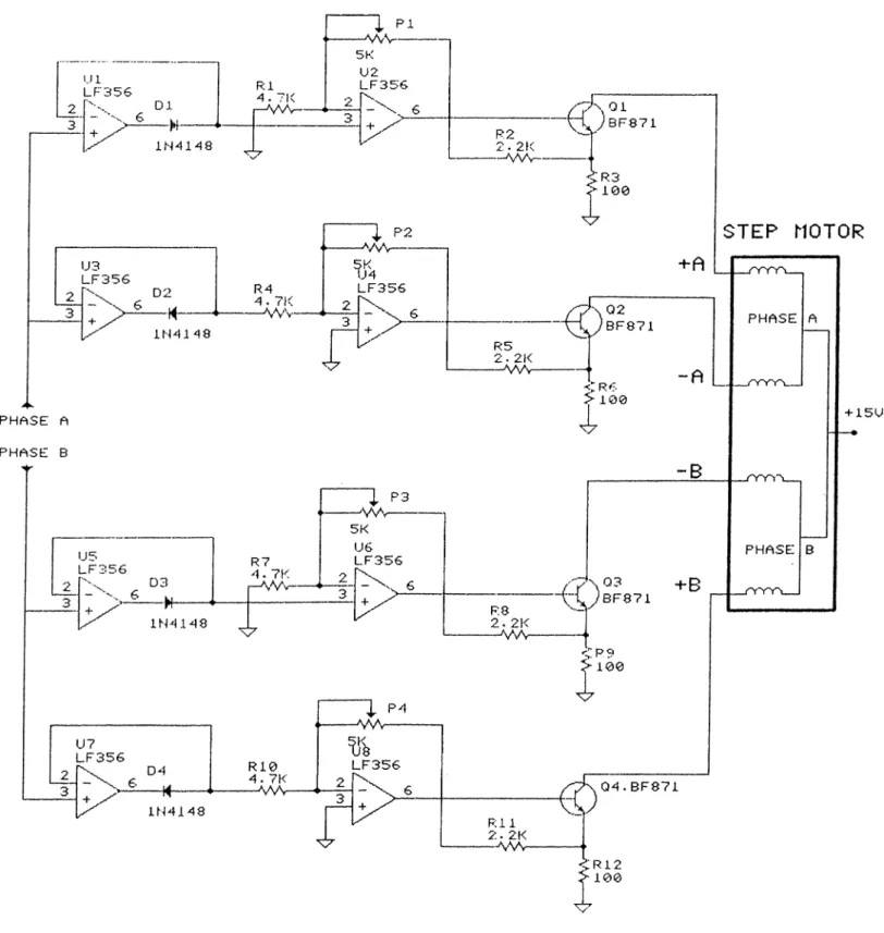
, lo- Therefore if we divide the period of the sine wave into smaller pieces, it makes smaller steps, i.e. microsteps. If the motor is machined precisely then the limiting factor is the driving electronics. One can make as many microsteps as he or she wishes. Our motor driving electronics, shown in Figure 3.6, processes the signals coming from computer and drives the coils of motor with predetermined current values. The desired signal is generated by two independent DACs in the data acquisition card [29] with a short subroutine. We can easily change number of microsteps within the software. We have achieved up to 200 microsteps with an unloaded motor. But when we load the motor by the nut , maximum number drops to 100. The smaller microsteps becomes unreliable. We have measured the size of microsteps with a Michelson Interferometer whose movable mirror is mounted on the sample holder which loaded the motor. For unloaded one, we have glued a mirror on the spindle and reflect a laser beam from that. The reflected beam is directed on the wall which is 4 m away from the mirror. Therefore small rotations of the spindle can be easily measured.Very recently, we have constructed a magnetically driven sample posi tioner [24], which will be described in detail elsewhere [30]. A small permanent magnet having three steel ball bearings at the bottom , stands on a microscope slide. A coil is placed under the slide. Application of pulsed currents to the coil exerts inertial jerks to the magnet on which the sample is mounted. Due to frictional forces the sample holder moves little bit and stops. Step size can be adjusted with the pulse duration. Steps as small as 5 nm are reproducible.
CHAPTER 3 . INSI'RUMENTATION 22
Figure 3.6. Motor Drive Circuit.
3.2.2
Scanner
The scanner is used to move the tip across the surface and to adjust the tunneling §np. Piezoelectric materials in various shapes aie widelj^ used foi this
CHAPTER 3. INSTRUMENTA1T0N 23
purpose. Important criteria for a high performance scanner can be summarized as follows:
• High Resolution : ~
0.1
A
in z direction, ~1
A
in x & y direction.• Large Scan Area ; ~ l/m i in all directions.
• Rigidity : necessary, for fast operation and immunity to disturbances.
• Cross Coupling : motion in one axis should not ciffect the others.
• Linearity : the motion of the scanner should be linear throughout its range.
Piezo bars attached in tripod form was the first STM scanner used by Binnig and Rohrer [9]. Wide variety of scanners have been developed by other groups. Bimorph driven tripod [31] in which circular bimorph elements drive an aluminum tripod, small piezo cubes assembled in matrix form to reduce the thermal drift [32], the popular single tube scanner developed by Binnig and Smith [35] and microscopic scanner in single chip STM [33], to name a few.
The single tube scanner is very small and rigid, therefore has resonant
CHAPTER 3. INSTRUMENTATION 24
frequencies as high as
8
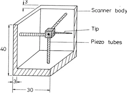
KHz. Outer electrode of a piezo tube is separated into four equal parts parallel to its axis as shown in Figure 3.7. The tube is mounted from its base. Elongation and contraction of one of the quadrants bends the end of the tube at which the tip is placed. Therefore tip can be scanned over the surface by applying appropriate voltages to the appropriate quadrants. Common electrode inside the tube can be used for z motion. Alternatively, z-voltage can be added to the quadrants. If the tip is mounted symmetrically for thermal drift compensation in x&y directions, symmetrical voltages should be applied to the opposing quadrants. Since single tube scanner is very simple and robust, it is very popular.Our scanner is constructed using small piezo tubes [34] which are glued in tripod form to an aluminum base and a
(1
x1
x1
) cm aluminum junction as shown in Figure 3.8. Tubes are 20 mm long with 3 mm OD and2
mm ID. A tip holder is clamped by a set screw to the junction. Outer electrodes are connected to the scanner base with conductive epoxy. Electrical connections to the tubes are also made by conductive epoxy and a Molex type connector mounted to the scanner base. The scanner body is mounted to the base of the microscope with two screws. Hence, scanner unit can be easily disconnected from the base.Although the tubes are expected to be identical, the tube’s sensitivities are measured by Michelson Interferometer as follows:
o
X : 45 T 10% y
y : 33 T 10% ^
o
z : 25 q= 10% ^ .
Our range is about 6000
A
with peak to peak voltage of 250 V from the output of high voltage amplifiers designed and implemented for this purpose. Since we usually keep the scanning range less than100
A,
hysteresis and creep do not cause any problem for most of the cases.CHAPTER 3. INSTRUMENTATION 25
Scanner body
Tip
Piezo tubes
3.2.3
Tip
Figure 3.8. Scanner Unit
The tip is the most critical part of the STM that directly determines the resolution. Tips are usually prepared from metal wires. Very sharp tips, usually single atom tips are necessary to obtain atomic resolution. On the other hand, quite dull tips must be used for Scanning Tunneling Spectroscopy because of Heisenberg’s uncertainty principle:
A k A x >
1
(3.4)If the tip is sharp (i.e. A x is small) then Ak is large. Therefore momentum, hence energy resolution of the tip is poor.
Although the radius of curvature of the tip may be quite large, a single atom sitting at the apex of the tip works as a very sharp tip. STM images are very closely related to the atomic structure of the tip. This dependence was predicted [36] and observed by different groups. Park et al. [37] have observed multiple tip effects on graphite sample. Kuk and Silverman have investigated for the first time how atomic structure of the tip affects STM images [38].
CHAPTER 3. INSTRUMENTATION 26
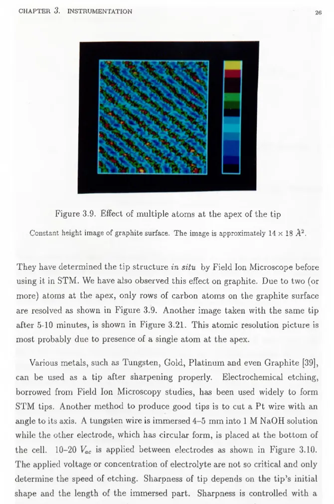
Figure 3.9. Effect of multiple atoms at the apex of the tip
Constant height image o f graphite surface. The image is approxiuiately 14 x 18 A~.
They have determined the tip structure in situ by Field Ion Microscope before using it in STM. We have also observed this effect on graphite. Due to two (or more) atoms at the apex, only rows of carbon atoms on the graphite surface are resolved as shown in Figure 3.9. Another imcige taken with the same tip after 5-10 minutes, is shown in Figure 3.21. This atomic resolution picture is most probably due to presence of a single atom at the apex.
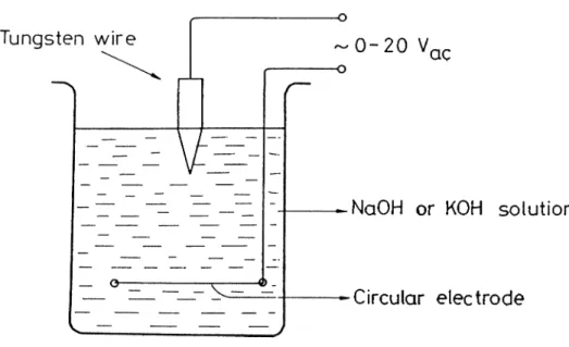
Various metals, such as Tungsten, Gold, Platinum and even Graphite [39], can be used as a tip after sharpening properly. Electrochemical etching, borrowed from Field Ion Microscopy studies, has been used widely to form STM tips. Another method to produce good tips is to cut a Pt wire with an angle to its axis. A tungsten wire is immersed 4-5 mm into
1
M NaOH solution while the other electrode, which has circular form, is placed at the bottom of the cell. 10-20 Vac is applied between electrodes as shown in Figure 3.10. The applied voltage or concentration of electrolyte are not so critical and only determine the speed of etching. Sharpness of tip depends on the tip’s initial shape and the length of the immersed part. Sharpness is controlled with a x240 optical microscope. The process is stopped when no finite radius canCHAPTER 3. INSTRUMENTATION 27
0 - 2 0 Vac
NaOH or KOH solution
•Circular electrode
Figure 3.10. Tip etching
be observed with the microscope. Tips produced by this method usually have some oxide layers at the surface therefore, some of them do not give atomic resolution. Ion Milling has been proposed to remove the oxide layer[40]. Most of the tips are reported to give atomic resolution after this process.
Tip fabrication is not very controllable. We can’t be sure which tip will give atomic resolution. Sometimes a fresh etched tip doesn’t work, but one day later one can resolve the Carbon atoms on Graphite surface with the same tip! STM tips are also not very stable. The tips can suddenly deform or reform and obtained image becomes poorer or better! There are some methods to clean deformed tips. We sometimes tap the marble block on which STM sits to achieve atomic resolution while it is running. Field Emission from tip with ~
100
V , a short voltage pulse to tip bias, letting it to scan for a long time are reported as a useful techniques for in situ tip cleaning [41].State of the art tip fabrication has been done by Fink [42]. He uses Field Ion Microscope to stick different atoms to the apex to produce very stable mono atomic tips. Those tips are used to generate monochromatic and focused electron beams.
CHAPTER 3. INSTRUMENTATION 28
h ( t )
d ( t )
Figure 3.11. Simplified STM control circuit.
3.3
The Control System
The simplified block diagram of the STM control system is shown in Figure 3.11. The tunneling current is converted to voltage, then linearized and compared with a reference current level by a logarithmic amplifier. Then, the resulting signal is amplified and integrated. This signal is applied to the z-piezo to regulate the tunnel gap.
In the constant current mode, the tip is scanned over the surface. Since the equilibrium gap changes due to surface corrugation, the tunneling current also changes. The control circuit should move the tip co establish the equilibrium tunnel gap.
Since we scan the tip over the sample, it is more appropriate to describe the surface corrugation as a function of time, h{t). The position of the tip, d(i), is measured from the equilibrium gap , sq, as shown in Figure 3.11. Therefore change in the gap distance is
CHAPTER 3. INSTRUMENTATION 29
The tunneling current is then
/ ( i ) = (3.6)
where /o(5o) is the reference current and ¡3 is the inverse decay length of the wavefunction in the barrier. The gain of the I-V converter , a V/A, only effects the equilibrium tunneling current and does not contribute to the loop gain. The gain and the reference level of the logarithmic amplifier is adjusted such that the output of the log amp is
^/
05(0
— (3.7)Therefore, we measure the change in the gap at the output of the logarithmic amplifier. The output of the integrator, which follows the logarithmic amplifier is
1
AM t) = (3.8)
where HC is the time constant of the integrator. The output voltage, which is applied to z-piezo is Wo
(0
■ bd A RC Jo[ As(T)dT , (3.9) Vo(t) = bd A RC Jof[d(r) - /i(r)]dr .
If we take time derivative of the above equation, we obtain
(3.10)
d , , bd . bd , , .
S c * * * * ■
(3.11)
This is the differential equation that relates the output to the input of the system.
CHAPTER O. INSTRUMENTATION 30
The position of the tip, c/(i), which is the output of the transducer, is related to the input of the transducer, Vo{t). This relation is cjuite complicated and can be described by the following convolution integral
/ +CC.
Vo{r)k{t — T)dn -OO
(3.12)
where k(t) is the impulse response of the trcinsducer. Then, Eq. 3.13 becomes
/,\ f+°° , ^ , bd , . . ^ ~ R C 7-00
dt RC (3.13)
Since an electromechanical transducer has infinite number of modes, the exact response of the transducer is quite complicated. Park and Quate [19] modeled the transducer with a delayed system
d(t) — kvinii — t) (3.14)
where k and r are the input voltcige, gain and delay time of the transducer, respectively. This approximation which ignores the resonant behavior of the transducer does not simplify, indeed complicates the necessary algebra. Because, a delayed differential equation must be solved for stability analysis.
The transducer can be modeled with a second order system quite accurately. In fact, our approach includes the previous one. Because, step response of a second order system has some delay. The Laplace transform of the k[t) is then.
i m =
kul
+ 2q;s + oJq (3.15)
where uq, cc and k are the resonance frequency damping factor and the gain of the piezo transducer, respectively, a is related to the quality factor, Q, of the piezo as follows
CHAPTER 3. INSTRUMENTATION 31
a = O/Q (3.16)
If we take Laplace transform of Eq. 3.17, we obtain
(3.17)
where Vo(s) and H {s) are the Laplace transforms of Vo{t) and h{t), respectively.
Output of the system can be found as a function of the input
K (s ) = bdjRCs
1
+ {bd/RCs)K{s) H (s ).(3.18)
If we define G{s) as
G{s) - bd
7
RCs s ’
(3.19)
then, Eq. 3.18 becomes
Vo(s) G ( s )
1 + G{s)K(s) H{s) (3.20)
The transfer function of the closed loop system is simply
T(s) =
G{3)
1 + G{s)K(s) '
(3.21)
The block diagram of the closed loop system is given in Figure 3.12. This is a typical feedback system that can be analyzed with standard control engineering tools [43]. The gain of the system,
7
, should be large for fast operation of the feedback loop. On the other hand, gain can not be increased indefinitely.CHAPTER 3. INSTRUMENTATION 32
V (s)
Figure
3
.12
. Block diagram of the Feedback System.because the S
3
''stem starts to oscillate. Therefore the maximum allowable gain should be determined as a function of system parameters.If the poles of the T(s) are in complex right-half plane then the system is unstable. Position of the poles of T (s), which is identical to the position of zeros of the denominator of T (s) on the complex s-plane, is plotted in Figure 3.13 for different gain values. The arrows show the movement of the poles as the loop gain increases. This method is called the Root-Locus Method [43].
... ...^ .3 ^ ... ... ...
■ w«
<1
»VCCHAPTER 3. INSTRUMENTATION 33
The maximum allowable loop gain is calculated to be COq
“ Q ■ (3.22)
The system starts to oscillate with frequency cuq at this gain. The critical
part of the system that limits the gain is the transducer. We need large loq and low Q for high performance. The performance of the system can be inci'eased by lowering the Q of the system by potting the piezo scanner [
44
].Our scanner’s specs are as follows
0 k = 25 A /V
0 cvq— 1.8 X 10'^ radjs
• Q ~ 10
3.4
Electronics and Computer Interface
The block diagram of the STM electronics is given in Figure 3.14. A bias voltage is applied to the tip and the tunneling current is measured from the sample. The scan signals are generated by two DACs under the computer control. The rough approach is controlled with a step motor driver described in previous sections.
The whole .system is ciccessible with a D T 2 8 2 1 —F data acquisition card [29] plugged in a P C /A T compatible computer. DT2821-F has two
12
-b it DACs, an8
-channel multiplexed 12-bit differential ADC ( Analog to Digital Converter ) and a 16-bit Digital I/O . DACs and ADC can be clocked up to200
KHz and 150 KHz, respectively.Step motor approaches the sample to the tip. Tip is retracted before ecich step to avoid crashing into the surface. After a step is completed, the tip is released. If the tunneling current is detected, then program takes care that the tip would stay within the z-scanner’s range by moving the sample back and
CHAPTER 3. INSTRUMENTATION 3-1
forth.
Figure 3.14. Block diagram of the STM electronics.
3.4.1
I - V Converter
The tunnel current is measured b}'' using a low input current O P -A M P as shown in Figure 3.15. Positive input of the O P -A M P is grounded and the tunnel current is applied to the negative input. A large feedback resistor, R f, is necessary to amplify very low tunneling currents. The output of the converter is then
CHAPTER 3. INSTRUMENTAl'ION 35 T I P UT GUf^RD RF
10
M — 0i
U1 LMll SAMPLE Ri 10K —^AV-R2 I00K — VvAr-U2
LF356 OUTPUT ---► ( TO RECTIFIER )Figure 3.15. I-V converter.
L M ll bipolar, CA3420 and CA3140 BiMOS O P-A M Ps were successfully used in our STM. Since the measured currents are very low, the printed circuit board must be carefully designed to eliminate the leakage and noise pickups. A guard ring which is connected to the ground, should be placed around the input pin to prevent the leakage currents. A coaxial cable should be used for connection from sample to the converter. The circuit and the whole STM must be shielded to reduce the hum. In addition, the current noise of the O P -A M P must be very low to reduce the noise level of the STM.
1
/ / noise is usually dominant for most of the amplifiers used. The gain of our converter is 100 m V /n A . The tunneling current is measured from a buffer amplifier, IC2
.3.4.2
z-Scanner Electronics
A home-made logarithmic amplifier is used to linearize the distance dependence of the tunnel current as shown in Figure 3.16. The input of the log amp must always be positive. Therefore, an active rectifier is used after the I - V converter. Output of the log amp is zero if the input current is 500/^A. Therefore, equilibrium tunnel current can be adjusted by R l and there is no need to use an additional comparator. Gain of the logarithmic amplifier is —1 V/decade.
CHAPTER 3. INSTRUMENTATION 36
Figure 3.16. z-scanner electronics.
of the integrator is adjusted by P3. LF398 Sample/Hold amplifier, which follows the integrator, is used to suspend the control temporarily. Then the signal is amplified with ICS whose gain can be adjusted by P i.
Resulting signal drives the z-piezo through a xlO high voltage amplifier. A High Voltage amplifier was designed using an OpAmp and a few transistors. The circuit diagram of the amplifier is shown in Figure 3.17. Swings of up to 250 Vpp can be obtained if one uses =[=150V supply. The range of the scanner is approximately 6000 A with this voltage swing. An ac coupled x40 amplifier, prior to the high voltage amplifier is used to record the piezo voltage. In addition, a buffer amplifier is used to record K
/10
at the input of the high voltage amplifier.CHAPTER 3. INSTRUMENTyVJTON 37
+ 140U
Figure 3.17. High Voltage Amplifier.
3.4.3
x&:y Piezo Driver
Raster scan signals in x and y direction are generated by two
8
-b it DACs as shown in Figure 3.18. The digital outputs of the data acquisition card are used to drive the converters. The image size is chosen to be 128 x 128 pixels. Therefore, LSBs of the DACs are grounded.The scan area is set by changing the reference input to the DACs. Two high voltage amplifiers are used to apply scan signals to the piezos. The gain of the amplifiers can be changed between
1
and 10. P2 and PZ are used to position the tip to a specific part of the surface by applying offsets to the amplifiers.CHAPTER 3. INSTRUMENTATION 38 L M 1 0 U1 P O S I T l U E R E F E R E N C E + 15U L·] 3 1 jL 4. F M F < 180K • T C I > R i N E G A T I V E R E F E R E N C E X - O F F S E T ( HU AM P ) ¥ Y - O F F S E T ( HU AMP ) ^ D T 2 8 2 1 - F DIO C7 1/ ~ L BIT S +5 U K r ; . D INP. 1 13 R9 lOK 5. . 12 15 U6 U<4 ^ W v - ^ L F35 6 M D A C 0 8 T ■ ) -- 1 5 U ^ 1 T - C 5 J 'J' 100NF N r h > TO X - H I G H U O L T A G E AMP TO Y - H I G H U O L T A G E AMP
Figure 3.18. x -y Scanner Electronics.
3.4.4
Data Acquisition
The global control of the system is performed by a personal computer. The program approaches the sample towards the tip to start the tunneling. Once the tunneling has started, it keeps the sample in the dynamic range of the z-piezo. The code was written in Turbo PASCAL 4.0.
The data can be acquired in various ways. In constant current mode, the tip is slowly scanned over the surface and the tip position, is recorded. The scan speed and gain of the reading is selected by the user. At each point, four voltage measurements are averaged to eliminate the noise.
On the other hand, the tip is scanned over the surface very fast while the tunnel current is recorded in the constant height inode. It is fast enough not
CHAPTER 3. INSTRUMENTATION 39
to give any chance to the control loop to regulate the gap variations. Total image acquisition time is
0
.4
s in this mode. The gain of the A /D conversions can be specified by the user.The data is stored in a 128 x 128 matrix. Top or
3
-D view is displayed just after the data is obtained. It is possible to store the images in data files for further processing. Previous images can also be read from the mass storage to make comparison between surfaces.3.4.5
Image Processing
Stored images are displayed and processed by another software. It is also written in Turbo PASC.AL 4.0 and requires an EGA monitor on an IBM compatible P C /X T or AT. Procedures of the program can be selected from the menu. Images are read from the mass storage. Dynamic range of the image is calculated and divided into 16 levels. Each level is assigned to a different color. Image is plotted as a top view or a 3-D view with the associated false color to the each level. x2 zoom in top view is another choice. The color code is plotted just near the images to help to the user.
Tilt and rotation angles might be changed by the user to view the surface from different directions in 3-D display. The hidden lines are also eliminated for a clear display. In addition, images having a slope in any direction can be corrected by the program.
3.4.6
Low Pass Filter
Usually, recorded images have some noise. A digital Low Pass Filter (LPF) was implemented to eliminate some part of the noise. Standard digital LPF design techniques were not chosen, because we must take FFT (Fast Fourier Transform) and inverse FFT for each filtering operation. Instead, a convolution LPF is implemented for its simplicity and speed. A convolution window given
CHAPTER 3. INSTRUMENTATION 40
W- 1, 0 W -,.,
W o , - , W o . o W o . i
W , . - i W , . o w , . ,
Figure 3.19. The convolution window.
in Figure 3.19 with coefficients u>ij is scanned over the image. The pixel values of the image are updated as follows
_Ylij ^ ‘j ^ ^x+i,y+j
A filtered image can be seen in Figure 3.20.
-
1
,0,1
(3.24)Figure 3.20. Low Pass Filter performance.
CHAPTER 3. INSTRUMENTATION 41
High Pass Filter can also be obtained easily, by changing the filter coefficients Uij. Moreover, Laplaciiin, Sobel or other, types of kernels might be used for the edge detection.
3.4.7
Median Filter
The data may sometimes be corrupted with spiky noise called Popcorn Noise. A LPF can not remove this type of noise. A Median Filter works very well for this purpose. A 3 x 3 window is scanned over the data matrix. The pixels just below the window are sorted and the median of this sequence is assigned to the central pixel. The Median Filter can not be described mathematically like a LPF. Figure 3.21 shows an image processed with a Median Filter.
Figure
3
.21
. Median Filter Performance.Chapter 4
Related Techniques and Applications
Invention of Scanning Tunneling Microscopy made a great impact on surface science. Beforehand, there was no tool to observe surfaces with the ultimate resolution. Various metal and semiconductors have been investigated first. Subsequentl)'^, biological samples, superconductors, adsorbed atoms on various surfaces etc. have been analyzed with STM.
Moreover, applications to the other fields started immediately. STM lithog raphy, Scanning Tunneling Spectroscopy, Scanning Tunneling Potentiometry, electrochemistry are some of the examples.
Other types of interactions between a probe and a sample in contrast to tunneling , can also be used for microscopy. SXM stands for those microscopes, where X denotes the type of the interaction. Interactions such as Optical near fields, interatomic forces, capacitance, ion flow, heat flow and evanescent optical fields were successfully used in SXM with resolutions ranging from
1
to1000 A.
In this chapter, we will review applications of STM and related techniciues, the SXM.