Growth of Ge nanoparticles on SiO
2
/Si interfaces during annealing
of plasma enhanced chemical vapor deposited thin films
S. Foss
a,⁎
, T.G. Finstad
a, A. Dana
b, A. Aydinli
ba
Department of Physics, University of Oslo, PO Box 1048-Blindern, N-0316, Norway
b
Department of Physics, Bilkent University, 06800 Ankara, Turkey Available online 16 January 2007
Abstract
Multilayer germanosilicate (Ge:SiO2) films have been grown by plasma enhanced chemical vapor deposition. Each Ge:SiO2layer is separated
by a pure SiO2 layer. The samples were heat treated at 900 °C for 15 and 45 min. Transmission electron microscopy investigations show
precipitation of particles in the layers of highest Ge concentration. Furthermore there is evidence of diffusion between the layers. This paper focuses mainly on observed growth of Ge particles close to the interface, caused by Ge diffusion from the Ge:SiO2layer closest to the interface
through a pure SiO2layer and to the interface. The particles grow as spheres in a direction away from the interface. Particles observed after 15 min
anneal time are 4 nm in size and are amorphous, while after 45 min anneal time they are 7 nm in size and have a crystalline diamond type Ge structure.
© 2006 Elsevier B.V. All rights reserved.
Keywords: Ge; Nanoparticle; Interfaces; Diffusion
1. Introduction
The underlying motivation of this work is control of nano-meter sized Ge-particle growth. A desired structure is an insulator in which nanometer sized Ge particles are embedded. Embedded semiconductor nanoparticles can find applications in optoelectronic devices [1–3] or charge storage devices[4–8]. The physical properties and ultimately the usefulness of the nanoparticles depend on the particle size and the particles' location with respect to other parts (interfaces, luminescent atoms, other nanoparticles etc) of a device. Ge has a relatively large excitonic Bohr radius of about 25 nm (compared to∼5 nm for Si). Thus quantum confinement effects can theoretically be observed over a relatively large and easy controllable range of nanocrystal sizes. The quantum confinement effects of most current interest are the size dependent energy levels and radiative transition probabilities. The energy levels of Ge
nanocrystals have recently been measured and modeled[9]. For memory applications of Ge nanocrystals the energy levels play an important role in the charging and discharging of nano-crystals and the control of the size and location of nanonano-crystals is a key element.
The formation of Ge nanocrystals in SiO2has been reported
by many authors using several different methods for the preparation of the nanocrystals such as ion implantation into SiO2[3,10], co-sputtering of Ge and SiO2[7,8], electron beam
evaporation of Ge sandwiched between SiO2[6], oxidation of
Si–Ge layers [11] or plasma enhanced chemical vapor depo-sition (PECVD)[12]. This paper presents a study of multilayer germanosilicate (Ge:SiO2) films made by plasma enhanced
chemical vapor deposition. Each Ge:SiO2layer, with different
Ge concentrations, is separated by a pure SiO2 layer. Such
multilayers are used in order to test Ge-particle growth in several layers at a time after annealing. This provides an efficient and time saving approach to obtain data on nano-particle growth. The present work focuses mainly on a phenomenon in which Ge atoms diffuse towards the interface between the film and the Si substrate and precipitation of Ge particles close to this interface. The diffusion in the films and
Thin Solid Films 515 (2007) 6381–6384
www.elsevier.com/locate/tsf
⁎ Corresponding author.
E-mail address:[email protected](S. Foss).
0040-6090/$ - see front matter © 2006 Elsevier B.V. All rights reserved. doi:10.1016/j.tsf.2006.11.094
the nanocrystal formation with respect to the interfaces could be different than those observed by other preparation methods for the films.
2. Experimental
The samples were prepared as six layers of germanosilacate (here notated as Ge:SiO2), sandwiched between silicon oxide
(SiO2) layers, and grown onto a polished single crystal (100) Si
wafer. The oxide films were deposited by a PECVD technique using a model PlasmaLab 8510C reactor. The PECVD process was carried out with the sample at 350 °C and process pressure of 1000 mTor under an applied RF power of 12 W. The process uses He and N2as carrier gases and precursor gases of SiH4,
NO2and GeH4. The flow rates were 200 sccm of SiH4(2% in
N2), 180 sccm of NO2for the SiO2layers and various flow rates
of GeH4(2% in He). The as deposited structure of the sample is
schematically shown inFig. 1. The first layer grown on the Si wafer, layer 0, was a pure SiO2layer followed by the Ge:SiO2
layer of highest Ge concentration, layer 1. Then follows pairs of layers of pure SiO2 and Ge:SiO2 with decreasing Ge
concentration, where only the Ge containing layers are num-bered. As indicated inFig. 1the GeH4flow rates were 120, 110,
100, 90, 80 and 70 for the six layers of Ge:SiO2. The nominal
concentration of these layers was determined from the calibration samples measured by photoelectron spectroscopy. The nominal Ge atomic concentrations of the layers are thus 0.132, 0.122, 0.115, 0.109, 0.092 and 0.08 as indicated inFig. 1. The wafer was cut in pieces and samples annealed in a dry N2
atmosphere at various temperatures. Here we report on 700 and 900 °C.
Transmission electron microscopy (TEM) specimens were made by gluing two substrates together with the film side facing each other. These samples were then cut and mechanically polished down to less than 50 μm in thickness. The samples
were subsequently ion milled until electron transparency using a 5 keV Ar+ion beam inclined at 5° angle from one side and 7° angle from the other side simultaneously. The TEM was a JEOL 2010F operated at an acceleration voltage of 200 keV. 3. Results and discussion
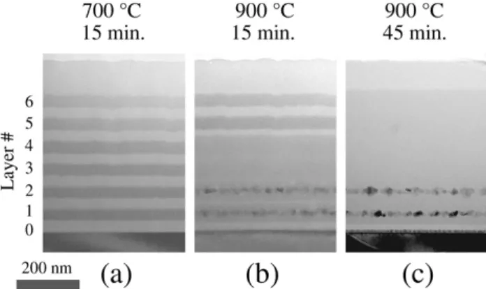
Fig. 2 shows cross-section TEM overview images of the
multilayered samples where sample A is annealed at 700 °C for 15, sample B is annealed at 900 °C for 15 min and sample C is annealed at 900 °C for 45 min. The layer numbering is also indicated in the figure. The contrast is due to increased absorption and scattering properties of heavier elements. The dark grey areas thus correspond to areas with high Ge content. FromFig. 2an interesting evolution of the contrast between the layers can be noted. All the Ge:SiO2 layers are clearly
distinguished for sample A annealed at 700 °C for 15 min. In the micrograph of sample B, which is annealed at 900 °C for 15 min, there is no contrast between layers 2 and 3 and also clearly much less contrast between layers 1 and 2 than there is in sample A. In the micrograph of sample C, there is no contrast between any layers. The changes in the contrast between the different layers are attributed to Ge diffusion within the SiO2film even if the concentration profiles of Ge
cannot be measured directly from the darkness of the micrographs. From the contrast one can see that a thin layer of low Ge content exists between layers 1 and 2 in sample B. There is no such layer visible between layers 3 and 4 in the same sample B. Even without considering the difference in overall Ge concentration in layers 1 to 2 versus layers 3 to 4, we can deduce that the Ge diffusion proceeds differently between these layer pairs. This difference in diffusion is further emphasized by considering the difference in overall Ge concentrations. The difference in diffusion behavior is attributed to the nucleation of Ge precipitates in layers 1 and 2, thus depleting the local SiO2solution of Ge.
Ge particles form in layers 1–2 of sample B and C, as shown in Fig. 2, and selected area diffraction (SAD) reveals the presence of a crystalline Ge diamond type structure in these layers. This is as anticipated and the multilayer structures have been used for
Fig. 1. Schematic drawing of the layered structure of the PECVD deposited films. The flow rates for GeH4are given in sccm as well as the nominal atomic
percentage in the layers.
Fig. 2. TEM micrograph overview of the samples. Samples A, B and C have different annealings. Dark and light grey areas correspond to high and low content of Ge, respectively. Precipitations of particles are seen in layers 1 and 2 of samples B and C.
studying the size distribution in the layers as a function of a wider annealing parameter variation than presently reported.
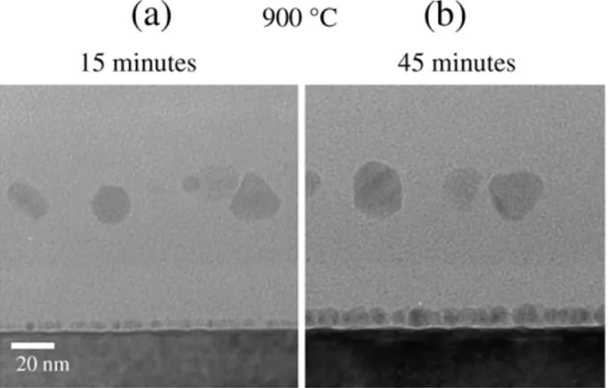
Nanoparticles have also been observed to grow in the vicinity of the Si/SiO2interface in samples B and C (annealed at
900 °C) as seen inFig. 3. The nanocrystals formed in layer 1 are large with some facets, while the particles formed near the interface appears more spherical. The latter particles have an average diameter of 4 nm after 15 min annealing time at 900 °C and are found to have an amorphous structure. Interface particles grown during 45 min annealing time at 900 °C have an average diameter of 7 nm and have a crystalline structure as can be seen from the lattice fringes inFig. 4. The nanocrystals have a random orientation with respect to the Si substrate. Their crystal structure has been identified as that of diamond crystal structure from SAD patterns as seen in Fig. 5 and the high resolution electron microscopy images ofFig. 4.
There seems to be a very little contact between the Si sub-strate and the Ge particles. It is however difficult to determine with precision whether these particles are in contact with the interface, since there would be a question whether the particles and the substrate are separated by∼1 nm of SiO2or if there is a
very small contact area. Contrast imaging is not a reliable tool in this case, because the contrast between the particles and the SiO2is diffused near the particle edge. We have analyzed the
high resolution electron microscopy (HREM) pattern of sample
C and examined whether the HREM pattern of the Ge crystals extends onto the HREM pattern of the Si substrate and this analysis shows that 25% of the particles (8 out of 32) have contact with the interface, and 75% (24 out of 32) do not. This analysis is not possible for sample B, in which the particles are amorphous. An explanation as to why some particles are not observed to have direct contact with the interface is that the cross-section analyzed in the micrographs are thin slices of the samples and the specimen surface can cut off the nanocrystals at various arbitrary planes, thus the actual percentage of nanocrystrals that are not in contact with the silicon substrate may be smaller than 75%.
Diffusion of Ge from layer 1 to the interface may be the source of the precipitated Ge close to the interface, referred to as the interface particles. A driving force for nucleation is an excess of Ge in the SiO2matrix. The excess Ge concentration
will not be the largest at the interface by a normal diffusion process and the particles' proximity to the interface indicates that the particles nucleate close to the surface because the interface (or something else in the vicinity of the interface) decreases the surface energy of the Ge nucleii. It may very well be that the particles nucleate onto the Si substrate itself, since
Fig. 3. Close up view of particles grown on the interface and Ge particles in layer 1. The interface particles are round and grow in a direction away from the interface.
Fig. 4. HRTEM image of two interface particles. The lattice fringes correspond to (111) Ge and (220) Ge.
Fig. 5. SAD of the substrate and the interface particles. Ge reflections are identified with 1% accuracy and are marked by grey circles.
Fig. 6. Illustration of a possible interface particle growth process. 6383 S. Foss et al. / Thin Solid Films 515 (2007) 6381–6384
the grain boundary energy would be less between Si and Ge than between SiO2and Ge. The accumulation of Ge at the Si/
SiO2interface has been reported before [10]. Avella et al.[11]
and Choi et al.[7]have reported nucleation of Ge nanocrystals close to a substrate surface, from a SiO2film with uniform Ge
concentration. Choi et al.[7]have argued that the formation of interface Ge particles could be influenced by Si diffusion through the SiO2film[13]and the Si substrate being the source
of the Si. Ge may then form by a reduction mechanism[14]. For nucleation onto the Si substrate, the expected shape of the particles is that of half-spheres rather than round particles. The half-sphere shape would be favored for the reduction of the grain boundary energy. What follows describes a possible explanation for the observed round shape in terms of the diffusion and precipitation process. Referring to Fig. 3, the particles seem to grow in a direction away from the interface. If extrapolating the data inFig. 3, the particles may start at a point at the interface or close to it, and then grow as spheres (see Fig. 6), keeping the initial contact between the particles and the interface at a near constant level. The growth rate in the direction towards the interface would be negligible. The growth rate in the direction away from the interface is highest and twice the rate of the growth in the direction parallel to the interface. The reason for this may be that during growth or nucleation of Ge particles, there would be a depletion of the local Ge concentration in the region surrounding the particles. Between two Ge particles in close proximity, there would be an overlap of the depletion zones. Consequently, the Ge concentration should be lower in the region between the particles. Since the Ge growth and the precipitation rate depend on the Ge concentration in SiO2, the fastest growth direction is away
from the interface. Between the particles the growth rate should be small, and even less closer to the substrate interface. It is also speculated whether a low mobility of Ge in a layer between the particles and the interface, for example a thin thermal SiO2
formed in the reactor during ramping up to the growth temperature for the deposition; a thermal oxide may be more dense than the deposited oxide and could limit Ge diffusion towards the interface and also the growth of the Ge particles into the substrate.
4. Conclusion
A multilayer GeSiO2 has been studied with a TEM.
Precipitation of Ge nanocrystals has been observed in the layers
of highest Ge. Evidence based on high contrast TEM images suggests a substantial degree of Ge diffusion in the sample. Precipitation of Ge particles close to an interface has been observed. The presence of Ge close to the interface is due to diffusion across a 40 nm layer. The nucleation process is unknown. The particles grow away from the interface as spheres. After 15 min annealing at 900 °C the particles are 4 nm amorphous particles. After 45 min 900 °C annealing, the particles are 7 nm crystalline particles.
Acknowledgement
This work was partly supported by the European Commis-sion through the project called SEMINANO under the contract NMP4-CT-2004–505285.
References
[1] G. Kartopu, V.A. Karavanskii, U. Serincan, R. Turan, R.E. Hummel, Y. Ekinci, A. Gunnaes, T.G. Finstad, Phys. Status Solidi, Appl. Mater. Sci. 202 (2005) 1472.
[2] C.L. Heng, T.G. Finstad, P. Storås, Y.J. Li, A. Gunnæs, O. Nilsen, Appl. Phys. Lett. 85 (2004) 4475.
[3] W. Skorupa, L. Rebohle, T. Gebel, Appl. Phys., A Mater Sci. Process. 76 (2003) 1049.
[4] S. Tiwari, F. Rana, H. Hanafi, A. Hartstein, E.F. Crabbe, K. Chan, Appl. Phys. Lett. 68 (1996) 1377.
[5] A. Dana, I. Akca, O. Ergun, A. Aydinli, R. Turan, J. Appl. Phys. (submitted for publication).
[6] C.L. Heng, T.G. Finstad, Physica E-Low-Dimens. Syst. Nanostruct. 26 (2005) 386.
[7] W.K. Choi, V. Ho, V. Ng, Y.W. Ho, S.P. Ng, W.K. Chim, Appl. Phys. Lett. 86 (2005) 143114.
[8] C.L. Heng, T.G. Finstad, Y.J. Li, A.E. Gunnæs, A. Olsen, P. Storås, Microelectron. J. 36 (2005) 531.
[9] Y. Nakamura, K. Watanabe, Y. Fukuzawa, M. Ichikawa, Appl. Phys. Lett. 87 (2005) 133119.
[10] E.S. Marstein, A.E. Gunnæs, U. Serincan, R. Turan, A. Olsen, T.G. Finstad, Surf. Coat. Technol. 158–159 (2002) 544.
[11] M. Avella, A.C. Prietoa, J. Jimemenez, A. Rodriguez, J. Sangrador, T. Rodrguez, Solid State Commun. 136 (2005) 224.
[12] S. Agan, A. Celik-Aktas, J.M. Zuo, A. Dana, A. Aydinli, Appl. Phys., A Mater. Sci. Process. 83 (2006) 107.
[13] Y. Maeda, Phys. Rev. B 51 (1995) 658.
[14] W.S. Liu, J.S. Chen, M.A. Nicolet, V. Arbet-Engels, K.L. Wang, J. Appl. Phys. 72 (1992) 4444.