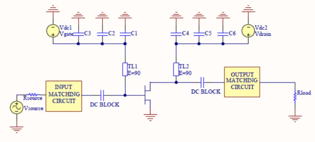
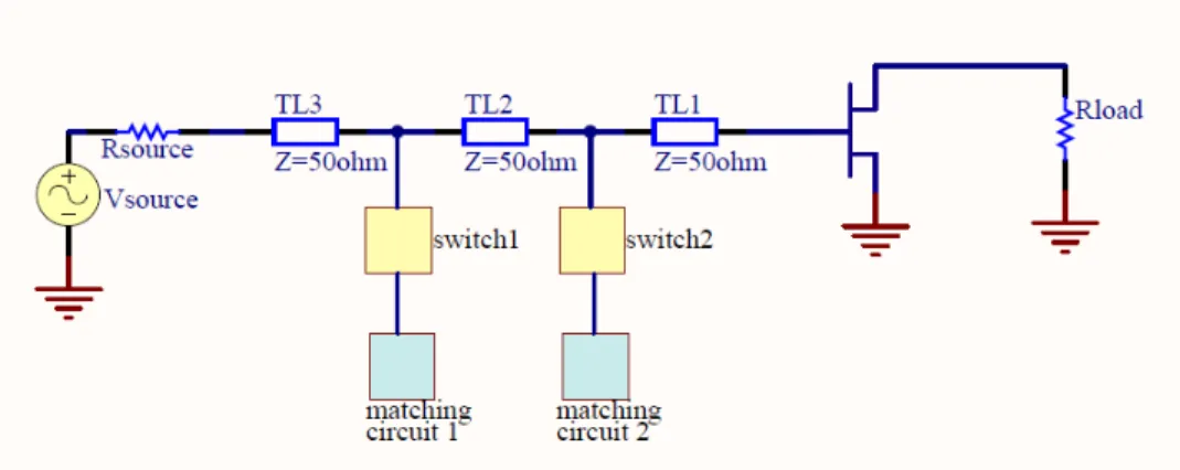
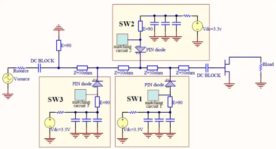
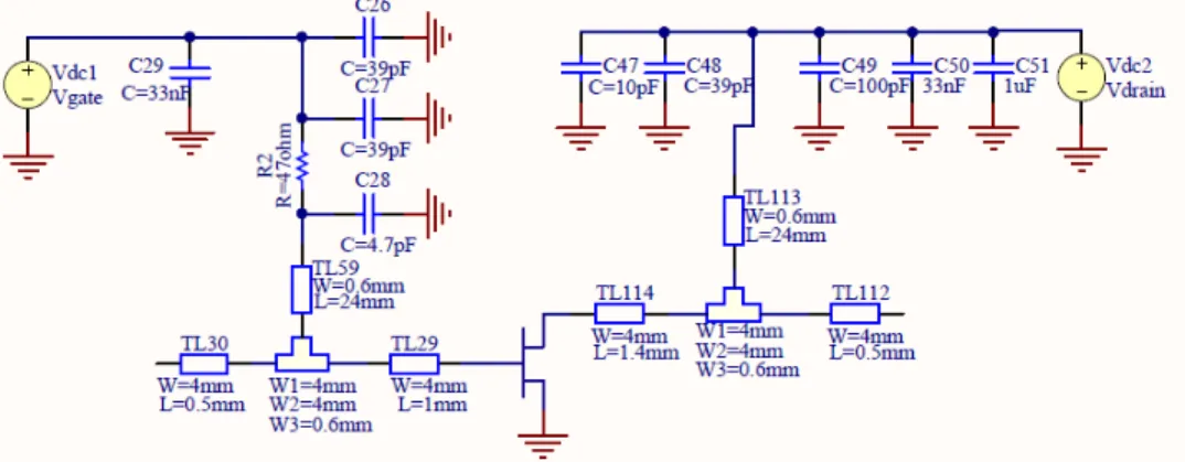
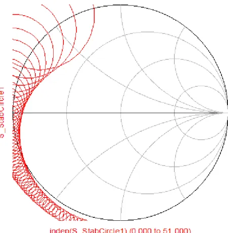
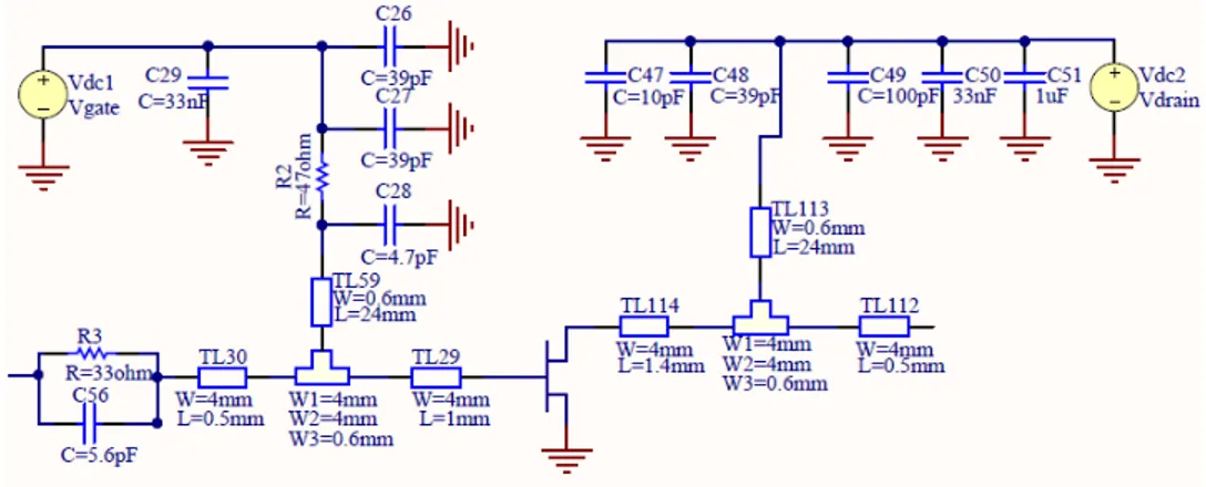
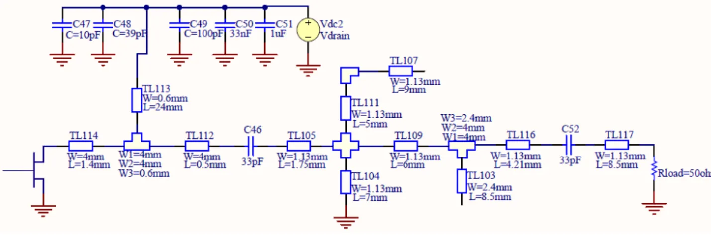
A band selecting UHF class-AB GaN power amplifier with 40 dBm output power
Tam metin
Şekil
Benzer Belgeler
However, the complexity of the structure and the fact that the piezoelectric we use is a ring rather than a full disk necessitate the use of finite ele- ment analysis to determine
Following fiber amplification, these pulses are used in micromachining titanium surfaces and compared to a picosecond and a nanosecond laser... Thus, the entire setup is
To summarize, we have employed the multicomponent generalization of the ladder approximation to study the short-range correlation effects in equal density double-wire
As well as the already standardized short-range wireless technologies discussed before, IEEE 802.15 is also working on the standardization of some recent technologies such as
Practical problems usually lead to very large systems of equations. To increase the efficiency of electrical circuit techniques, model order reduction techniques may
Should terrorism be defined as a legal concept or, is it preferable to define the criminal acts that take part in the actions taken by terrorist organizations separately
We have developed a mathematical model which con- currently selects product design, generates process plans and develops production plans to minimize the sum of processing cost,
We asked four observers to compare the glossiness of pairs of surfaces under two different real- word light fields, and used this data to estimate a transfer function that captures
