Micromachined two-dimensional array piezoelectrically actuated
transducers
Gökhan Perçin, Abdullah Atalar, F. Levent Degertekin, and Butrus T. Khuri-Yakub
Citation: Appl. Phys. Lett. 72, 1397 (1998); doi: 10.1063/1.121067 View online: http://dx.doi.org/10.1063/1.121067
View Table of Contents: http://apl.aip.org/resource/1/APPLAB/v72/i11
Published by the American Institute of Physics.
Related Articles
Electroacoustic response of 1-3 piezocomposite transducers for high power applications
Appl. Phys. Lett. 101, 253504 (2012)
Three-dimensional micro electromechanical system piezoelectric ultrasound transducer
Appl. Phys. Lett. 101, 253101 (2012)
Efficient counter-propagating wave acoustic micro-particle manipulation
Appl. Phys. Lett. 101, 233501 (2012)
Piezoelectric and electrostrictive effects in ferroelectret ultrasonic transducers
J. Appl. Phys. 112, 084505 (2012)
Piezoelectric resonator arrays for tunable acoustic waveguides and metamaterials
J. Appl. Phys. 112, 064902 (2012)
Additional information on Appl. Phys. Lett.
Journal Homepage: http://apl.aip.org/Journal Information: http://apl.aip.org/about/about_the_journal
Top downloads: http://apl.aip.org/features/most_downloaded
Information for Authors: http://apl.aip.org/authors
Micromachined two-dimensional array piezoelectrically
actuated transducers
Go¨khan Perc¸in,a)Abdullah Atalar,b)F. Levent Degertekin, and Butrus T. Khuri-Yakub
Edward L. Ginzton Laboratory, Stanford University, Stanford, California 94305-4085 ~Received 16 December 1997; accepted for publication 20 January 1998!
This letter presents micromachined two-dimensional array flextensional transducers that can be used to generate sound in air or water. Individual array elements consist of a thin piezoelectric ring and a thin, fully supported, circular membrane. We report on an optimum design for an individual array element based on finite element modeling. We manufacture the transducer in two-dimensional arrays using planar silicon micromachining and demonstrate ultrasound transmission in air at 2.85 MHz. Such an array could be combined with on-board driving and an addressing circuitry for different applications. © 1998 American Institute of Physics.@S0003-6951~98!03911-4#
Two-dimensional arrays of ultrasound transducers are desirable for imaging applications in the fields of medicine, nondestructive evaluation, and underwater exploration. Mak-ing arrays of transducers by dicMak-ing and connectMak-ing individual piezoelectric elements is fraught with difficulty and expense, not to mention the large input impedance mismatch problem that such elements present to transmit/receiving electronics. Our approach is to use micromachined flextensional piezo-electric transducers. Individual elements are made of thin silicon nitride membranes covered by a coating of piezoelec-tric zinc oxide ~ZnO!. The arrays are made by using silicon micromachining techniques and are capable of operation at high frequencies. Inherently, this approach offers the advan-tage of integrating transducers with transmitter and receiver electronics. Thus, we present arrays where elements can be individually addressed for ease of scanning and focusing by using on-board electronics.
We fabricated micromachined piezoelectrically actuated flextensional transducers in a 2-D array by combining con-ventional IC manufacturing process technology with ZnO deposition. Individual array elements consist mainly of a cir-cular membrane attached to a circir-cular ring of piezoelectric material which has optimized dimensions. An ac voltage is applied accross the piezoelectric material to set the com-pound membrane into vibration. At the resonant frequencies of the compound membrane, the displacement at the center is large.
We design the individual array element to have a maxi-mum displacement at the center of the membrane at the reso-nant frequency~Perc¸in et al.1,2!. Analyses of similiar devices such as those of Allaverdiev,3 Vassergiser et al.,4 Okada et al.,5and Iulo et al.,6are helpful in identifying the impor-tant parameters of the device. However, the complexity of the structure and the fact that the piezoelectric we use is a ring rather than a full disk necessitate the use of finite ele-ment analysis to determine the resonant frequencies of the structure, the input impedance of the transducer, and the nor-mal displacement of the surface.
It is well known that the transverse displacementjof a simple membrane of uniform thickness, in vacuum, obeys the following differential equation:7
¹4j1 r D
]2j
]t250 ~1!
The axisymmetric free vibration frequencies for an edge-clamped circular membrane are given by
v5 l
2
a2
Ar
/D, ~2!
wherel represents the eigenvalues of Eq. ~1!, a is the radius of the membrane, r is the mass per unit area of the mem-brane, and
D5 Eh 3
12~12n2!, ~3!
where E is Young’s modulus, h is the membrane thickness, andn is Poisson’s ratio.
By substituting typical dimensions for the individual ar-ray element of the above equations and by using average values for h, E, n, andr, we obtain the first resonance fre-quency at 2.62 MHz, which is a reasonable approximation to 2.8–3.0 MHz that was measured in our experiments. The above equations suggest that the resonant frequency is di-rectly proportional to the thickness of the membrane and inversely proportional to the square of the radius. However, it is also known that the resonant frequency will be decreased by fluid loading on one or both sides of the membrane. The shift in the fluid loaded resonant frequency of a simple mem-brane is shown by Kwak8 to be
fw5 fa
A
11bG, ~4!whereb5rwa/rmh is a thickness correction factor,rwis the
density of the liquid, rm is the mass density of the circular
membrane, andG is the non-dimensional added virtual mass incremental~NAVMI! factor, which is determined by bound-ary conditions and mode shape. For the first order axisym-metric mode and for water loading on one side of the
mem-a!Electronic mail: [email protected]
b!Department of Electrical and Electronics Engineering, Bilkent University, Bilkent 06533, Ankara, Turkey.
APPLIED PHYSICS LETTERS VOLUME 72, NUMBER 11 16 MARCH 1998
1397
0003-6951/98/72(11)/1397/3/$15.00 © 1998 American Institute of Physics
brane, G is 0.75. Assuming the composite will behave similarly to the single membrane, we expect the resonant frequency to shift down by 63% for one of our devices.
We designed micromachined two dimensional array transducers by modeling one element large scale prototype
~Perc¸in et al.1,2!. However, the two-dimensional array nature
of the device is accomodated by a suitable micromachining process. Materials are chosen in accordance with availability of micromachining and IC manufacturing processes. Other piezoelectric materials, membrane materials, electrode met-als, and substrates can be used.
We used ANSYS to optimize an individual array ele-ment made with piezoelectric ZnO on a silicon nitride mem-brane. Several iterations were run to maximize the displace-ment of the membrane as a function of the dimensions of the piezoelectric ring. Maximum displacement was obtained when the piezoelectric ring had an inner diameter of 30mm and outer diameter of 80mm with a thickness of 0.3mm, and the silicon nitride had a diameter of 100mm with a thickness of 0.3mm. The dc displacement is 2.27 Ao/V. The resonance
frequency 3.46 MHz obtained from ANSYS simulation in vacuum is a good approximation to 3.07 MHz that was mea-sured in vacuum with one of our devices.
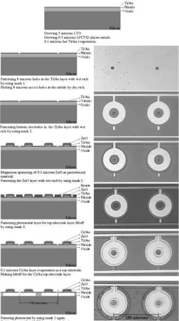
The fabrication process for micromachined two-dimensional array flextensional transducers is given in Fig. 1. At the right side of the figure, actual pictures of two ad-jacent elements from a two-dimensional array are given along with the process flow. The process starts with growing a sacrificial layer, chosen to be silicon oxide~8% phosphorus doped densified LTO!. A membrane layer of low-pressure chemical vapor deposition~LPCVD! silicon nitride is grown on top of the sacrificial layer. The bottom Ti/Au electrode layer is deposited on the membrane by e-beam evaporation at 228 °C. The degree to which the ZnO c-axis, ^0002&, is ori-ented normal to the substrate surface is very sensitive to the degree to which the Au film is^111& oriented. The quality of the ZnO is measured by an x-ray rocking curve scan. The ZnO had a 5.5°-wide rocking curve above Au with a 5°-wide rocking curve. The bottom metal layer is patterned by wet etch, and access holes for sacrificial layer etching are drilled in the membrane layer by plasma etch. Later, the bottom electrode layer is patterned by wet etch, and a piezoelectric ZnO layer is deposited on top of the bottom electrode. The ZnO is deposited by dc planar magnetron reactive sputtering from a 127-mm-wide target consisting of 99.99% Zn. The deposition is made in an 20%–80% argon-oxygen ambient with a flow rate of 26.6 sccm, a pressure of 7 mTorr, a substrate temperature of 145 °C, and a dc power of 350 W. The separation between the substrate and the target is 51 mm. The depositon rate is 9.0 Ao/s. The top Cr/Au electrode layer is formed by e-beam evaporation at room temperature and patterned by liftoff. The last step is etching the sacrificial layer by wet etch, and this concludes the front surface mi-cromachining of the devices. Figure 2 shows final 60360 two-dimensional array devices. The die size is 1 cm31 cm.
Figure 3 shows the real part of the electrical input im-pedance of only one row of 60 elements of devices shown in Fig. 2. Operating in air, the transducers have a resonant fre-quency of 3.0 MHz and a fractional bandwidth of about 1.5%. The real part of the electrical input impedance has a 280 V base value, and it was determined by SPICE simula-tion that this base value is caused by the bias lines
connect-FIG. 1. Realized micromachined device process flow.
FIG. 2. Realized micromachined device.
1398 Appl. Phys. Lett., Vol. 72, No. 11, 16 March 1998 Perc¸inet al.
ing individual array elements. This can be avoided by using electroplating to increase the thickness of the bias lines. Fig-ure 3 also shows the existence of acoustical activity in the device, and an acoustic radiation resistance Ra of 150 V.
Figure 4 presents the change of the electrical input imped-ance in vacuum of a device consisting of one row of 60 elements. The resonance frequency is 3.00 MHz in air and 3.07 MHz in vacuum ~at 50 mTorr!. This result is in accor-dance with our expectations, since the resonant frequency and the real part of electrical input impedance at resonance should increase in vacuum. The acoustic activity in vacuum reflects energy coupling to the structure. This is a major
source of loss in the device and is a present topic of research in our group. Figure 5 shows the result of an air transmission experiment where an acoustic signal is received following the electromagnetic feedthrough. The insertion loss is 112 dBs. In the transmit/receive experiment, the receiver had one row of 60 elements, and the transmitter had two rows of 120 elements. Loss due to eletrical mismatches is 34.6 dBs. Other important loss sources are alignment of receiver and transmitter, and structural losses.
In summary, we have developed a novel ultrasonic trans-ducer which is silicon micromachined into two-dimensional arrays. The individual array element is based on a variation of a flextensional transducer. The transducer design was op-timized using finite element analysis, and the ultrasonic transmission was demonstrated in air.
This research was supported by the Defense Advanced Research Projects Agency of the Department of Defense and was monitored by the Air Force Office of Scientific Research under Grant No. F49620-95-1-0525.
1
G. Perc¸in, L. Levin, and B. T. Khuri-Yakub, IEEE Ultrasonics Sympo-sium, November 3–6, 1996.
2G. Perc¸in, L. Levin, and B. T. Khuri-Yakub, Rev. Sci. Instrum. 68, 4561 ~1997!.
3A. M. Allaverdiev, N. B. Akhmedov, and T. D. Shermergor, Prikl. Mat. Mekh. 23, 59~1987!.
4M. E. Vassergiser, A. N. Vinnichenko, and A. G. Dorosh, Sov. Phys. Acoust. 38, 558~1992!.
5H. Okada, M. Kurosawa, S. Ueha, and M. Masuda, Jpn. J. Appl. Phys., Part 1 33, 3040~1994!.
6
A. Iula, N. Lamberti, G. Caliano, and M. Pappalardo, IEEE Ultrasonics Symposium, November 1–4, 1994.
7A. W. Leissa, Vibration of Plates~Scientific and Technical Information Division, Office of Technology Utilization, NASA, 1969!, pp. 1–10. 8
M. K. Kwak, J. Sound Vib. 178, 688~1994!. FIG. 3. Electrical input impedance real part of the realized micromachined
device.
FIG. 4. Electrical input impedance real part change of the device in vacuum and air.
FIG. 5. Air transmission/receive experiment of the realized micromachined device.
1399
Appl. Phys. Lett., Vol. 72, No. 11, 16 March 1998 Perc¸inet al.