45
J.P. Blitz and V.M. Gun’ko (eds.), Surface Chemistry in Biomedical and Environmental Science, 45 58. © 2006 Springer.
EXTERNAL STIMULI
GULAY ERTAS, SEFIK SUZER*
Bilkent University, Department of Chemistry and the Laboratory for Advanced Functional Materials, 06800 Ankara, Turkey
Abstract. X-ray Photoelectron Spectroscopy, XPS, due to the perfect match of its probe length (1-10 nm) to nanoparticle size, chemical specificity, and suscepti-bility to electrical charges, is ideally suited for harvesting chemical, physical and electrical information from nanosized surface structures. In addition, by recording XPS spectra while applying external d.c. and /or pulsed voltage stimuli, it is also possible to control the extent of charging and extract various analytical information. In the simplest form, application of a static (d.c.) voltage stimuli enhances separation of otherwise overlapping peaks of gold nanoparticles from that of metallic gold. When the voltage stimuli is applied in the form of rectangular pulses, dynamic information is obtained from the frequency dependence of the charging shifts. This enables us to better probe the composition of nanoparticles produced (i.e. silicide formation, or whether or the extent of reduction, etc.) when platinum salt is deposited on silicon substrates. Finally, by recording the data in different time windows, XPS spectra can be recorded in time-resolved fashion. Time-resolved spectra can be used to detect, locate and quantify the charges developed in various surface structures like gold(core)/ silica(shell) nanoparticles on a copper substrate.
Keywords: XPS; differential charging; peak separation; time-resolved XPS
1. Introduction
XPS is one of the most widely used surface analysis techniques for extracting ______
*To whom correspondence should be addressed. S. Suzer, Bilkent University, Department of Chemistry and the Laboratory for Advanced Functional Materials, 06800 Ankara, Turkey; e-mail: [email protected]
– information related to the chemical nature of surface structures on the
nanometer scale. This 40+ year old technique consists of irradiation of the sample with x-rays causing photoelectrons to be emitted from the sample surface, and subsequent determination of their kinetic energies by an energy analyzer. The binding energies are obtained using the energy of the x-ray, and Einstein’s equation (B.E. = hȣ – K.E.), which leads to determination of elemental identities and chemical states. Surface sensitivity stems from the attenuation length of the photoelectrons (1-10 nm) within the solid samples. Except for hydrogen, all elements can be unambiguously identified.1
The photoelectrons ejected leave positive charges behind, which are normally replenished via the ground loop of a conducting sample. For non-conducting or poorly non-conducting samples this process is slow. Positive charging develops which decreases the kinetic energy of the photoelectrons, hence increasing the apparent binding energies.2-6 For uniform samples this is not a problem, since charge correction can be accomplished using a suitable reference. For heterogeneous or layered samples with different conductivities, this problem is severe and manifests itself as differential charging. Flooding the sample with low energy electrons or ions has been successfully used for neutralizing the positive charges developed.7-11 Complete elimination of this problem is only an ideal, and overneutralization leading to negative charging has also been encountered.
A number of publications have appeared reporting constructive use of this surface charging (mostly negative) phenomenon for elucidating chemical and/or structural parameters of various materials. Lau and coworkers have studied the structural and/or electrical properties of ultrathin dielectric films on semi-conductors utilizing the surface-charging.12-18 Thomas et al. separated the surface spectrum (mainly silicon dioxide) from the silicon substrate spectrum (consisting of contamination and silicon dioxide on silicon), by use of surface charging.15,16,19 Similar applications were also reported by Ermolieff et al.20 and Bell and Joubert,21 while Miller et al. applied the technique to separate the XPS signals of the fiber from the exposed matrix at fractured surfaces.22 Elegant use of surface charging for lateral differentiation of mesoscopic layers, and for depth profiling in 1-10 nm thin layers, have recently been reported.12,23,24 Surface-charging was invariably controlled/varied via a low energy electron flood gun, resulting in mostly negatively charged surfaces. We have recently demonstrated that useful information can also be extracted by analysis of positively charged surfaces. We do not attempt to neutralize the charging developed, and achieve enhanced positive charging by application of a negative voltage bias to the sample while recording the XPS spectrum.25,26
Application of external bias to the sample goes back 3 decades.5 However, using an external bias for extracting chemical and/or structural information is scarce. One successful application demonstrated that biasing the sample holder
with a large negative d.c. voltage (25-100V) could be used to identify chemical differences in oxide films on an aluminum alloy.27 Similarly, we have recently reported that application of a small (1-10V) negative bias leads to enhanced differential charging by repelling stray electrons or electrons emitted from a nearby filament. A positive bias reduces charging between the oxide layers and the underlying metal substrates.28,29
2. Experimental
Oxide layers were grown thermally on HF-cleaned Si (100) substrates at 500°C in air. Citrate-capped gold nanoclusters were prepared according to a well-established procedure and were directly deposited from their aqueous solutions onto the SiO2/Si substrates.
30,31
A Kratos ES300 electron spectrometer with MgKα x-rays (nonmono-chromatic) was used for XPS analysis. A typical sample was a ca. 1mm-thick at 45o, and emits photoelectrons at 90o with respect to its surface plane. The sample can also be rotated to decrease the emission angle to enhance surface sensitivity, while keeping the x-ray-sample-analyzer angle at 45o. Calibration of the energy scale was carried out using standard silver and gold samples, referencing to the C1s peak at 285.0 eV. Resolution of the spectrometer was better than 0.9 eV measured with the Ag3d peaks, and standard curve fitting routines were used with 0.6 eV spin-orbit parameter for the Si2p peak.
3. X-Ray Photoelectron Spectroscopy under External Stimuli
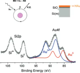
The power of the XPS technique as an analytical tool is related to both its chemical and state (i.e. ionic charge) specifity, and its applicability to all elements except H. The XPS spectrum of a silicon substrate containing ca. 4 nm oxide layer, grown thermally on top of which an aqueous solution containing 10–4 M HAuCl4 is deposited and dried in air, is shown in Figure 1. Both the Si2p and Au4f peaks are composed of two chemically different species. For silicon, the peak at lower binding energy (99.5 eV) corresponds to the silicon substrate underneath, and the peak at 104 eV corresponds to the thermal oxide layer (SiO2). The Au4f has a 3.6 eV spin-orbit splitting. The composite peak can be fit with 2 doublets (Au4f7/2– 4f5/2
ionic (Au3+) and reduced (Au0) forms of gold. Quantification, as well as overlayer thickness, can be obtained from peak intensities.1 Measured binding energies contain components from both the chemical shift, related with silicon wafer with dimensions of 4 x 12 mm. The sample normally accepts x-rays
chemical state of the elements, and charging effects. This can be very misleading if the two are not separated properly. For example, the true binding energy difference between the Si4+ and the Si0 peaks is 3.2 eV, almost 1 eV smaller than measured, and can vary from –1 to about 5 eV depending on the extent of neutralization.32,33 As will be shown below, this shift can also be influenced by application of an external bias to the sample rod. The binding energy also depends on the size/shape of the metallic clusters, offering a new analytical dimension.34,35
Figure 1. Part of the XPS spectrum
showing the Si2p-Au4f peaks of a silicon substrate containing ca. 4 nm thermal oxide layer with one drop of 0.0001 M aqueous solution of HAuCl4
deposited, and dried in air. The silicon peaks corresponding to the silicon substrate (Si0) and the silicon oxide layer (Si4+), as well as two different chemical state of gold (Au3+ and Au0) are clearly resolved.
3.1. STATIC STIMULUS (D.C. BIAS)
In conventional XPS the sample is grounded. In our technique, a voltage bias to the electrically isolated sample rod is applied. Under negative bias the spectrum
Figure 2. Figure 1 spectra
under +10V, grounded, and -10V after complete reduction with x-rays. Application of an external stress results in asymmetrical peak shift. shifts to higher kinetic energy (blue shift), the shift is to lower energy (red shift) under positive bias. This is shown in Figure 2 for the same
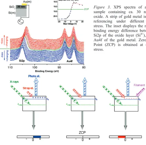
silicon/silicon oxide sample after complete reduction by x-rays.36 Whereas the Si0 peak shifts exactly 10 eV, the shift in both the Si4+ and the Au4f peaks differ from differential charging developed in the oxide layer. Figure 3 shows spectra of a silicon sample with a 30 nm thick oxide layer. A gold metal strip is tied to the sample for referencing. The spectra are shifted with respect to Au4f peaks, where the value of the Au4f7/2 peak is set to 84.0 eV.
1
In this case, the silicon substrate peak (Si0) is too deep to be observed. The inset in Figure 3 shows the measured binding energy difference between the Si2p of the oxide, and the Au4f peaks as a function of the applied bias. Under negative bias all electrons which cause partial neutralization are repelled to yield a positively charged oxide layer. This leads to a larger binding energy difference between the Si2p and Au4f peaks.
Figure 3. XPS spectra of a silicon
sample containing ca. 30 nm thick oxide. A strip of gold metal is tied for referencing under different voltage stress. The inset displays the measured binding energy difference between the Si2p of the oxide layer (Si4+), and the Au4f of the gold metal. Zero Charge Point (ZCP) is obtained at ca. +1V stress.
Figure 4. Schematic representation of the charging process. 3 different currents flow from the
sample to the spectrometer due to; (i) photoelectrons generated by x-rays, (ii) stray electrons from the x-ray tube and/or other elements within the vacuum chamber, and (iii) low energy electrons from a nearby filament.
Zero charging point (ZCP) corresponds to a 19.4 eV difference. So the correct binding energy of Si2p (103.4) is obtained only under ca. +1 V bias. Larger positive biasing leads to negative charging of the oxide layer as shown schematically in Figure 4. External bias (d.c.) is a simple technique for controlling the extent and polarity of ultra-thin oxide layer charging. This can be used as an analytical tool for peak separation, or extracting information related to the proximity of atoms in nanometer-scale surface structures.25,37 Representative analytical applications will be given later.
3.2. DYNAMIC (PULSED) STIMULUS
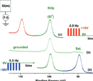
The application of external stimuli in rectangular pulses provides additional advantages. Figure 5 depicts the Si2p region of an HF-cleaned Si (100) sample containing 1 nm thick native oxide layer. During one pulse, the sample spends 50% of its time near ground potential, and 50% of its time at +10V. Therefore all peaks are twinned at all frequencies (0.1 to 1000 Hz), and with exactly the same energy difference (10 ± 0.1 eV).
Figure 5. XPS spectra of the
Si2p region of a clean silicon surface (Si0) recorded by: (b)
grounding the sample, (a) applying 0 to –10V pulses at 0.1 Hz, (c) applying 0 to +10 V pulses at 0.1 Hz. The Si0 peak is twinned, because when pulsed the sample experiences the ground and the applied potential 50% at a time. Sat. refers to peaks of the KĮ3,4 x-ray satellites.
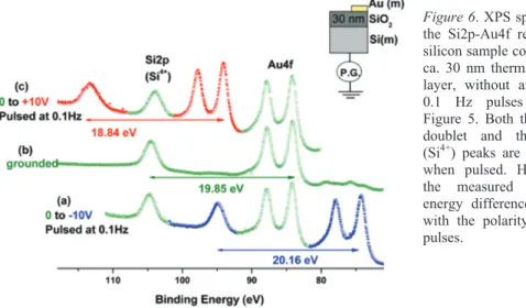
The situation is very different when the oxide layer is larger than 2 nm and the measured energy differences vary with the pulse frequency due to differential charging. To calibrate the measured energy differences a gold metal strip in electrical contact with the sample is used. In Figure 6 we show the Si2p-Au4f region of a sample containing a 30 nm thermal oxide layer. The measured binding energy difference between the Si2p of the oxide layer (Si4+), and the Au4f, are different in all the three cases [i.e. (b) grounded, under (a) negative
and (c) positive pulses respectively]. In the negative cycle the slow stray electrons, or electrons from the filament are repelled. The oxide layer is left positively charged to cause the measured binding energy difference to increase. In the positive cycle, the low energy electrons are withdrawn onto the sample to neutralize the oxide layer and decrease the measured binding energy difference. In this particular experiment the oxide layer is overneutralized and negatively charged since the measured ∆B.E. is 18.84 eV, which is smaller than the actual value of 19.4 eV (103.4 eV for Si2p of the oxide minus 84.0 for Au4f ).
Figure 6. XPS spectra of
the Si2p-Au4f region of silicon sample containing ca. 30 nm thermal oxide layer, without and with 0.1 Hz pulses as in Figure 5. Both the Au4f doublet and the Si2p (Si4+) peaks are twinned when pulsed. However, the measured binding energy difference varies with the polarity of the pulses.
The measured binding energy difference changes with the pulse frequency. The difference is small at high frequencies, due to the rapid changes of the applied voltage between ground and +10V. The oxide layer cannot respond quickly enough and an average potential throughout the cycle is measured. At low frequencies the measured binding energy difference, between the Si2p and the Au4f levels under positive pulses, becomes smaller when compared to ground, since more time is allocated for the silicon oxide layer to neutralize its positive charge.
3.3. TIME RESOLVED MEASUREMENTS
It is possible to record data in different time windows after the application of a pulse to obtain time-resolved spectra. The pulses are applied to the sample rod externally using a digital-to-analog converter (DAC), and the photoelectrons are amplified and counted for a given period. The kinetic energy axis of the spectrometer is also controlled by the DAC. Each measurement starts by setting the kinetic energy to the first point with application of +10V to the sample rod.
We then apply 4 repetitive steps: (1) wait for 2.5 s for equilibration; (2) apply – 10V; (3) recording data in 5 ms intervals for 1 s in separate columns for 200 data points. Return to +10V; (4) increment the energy to restart the cycle. One spectrum scan is completed after repeating these cycles for the entire XPS region. Since only 10-50 counts are collected signal averaging is necessary. Typically 50-250 scans are recorded, requiring 3-15 hours. This procedure results in a collection of 200 spectra recorded with 5 ms time resolution. In principle the time resolution is limited only by the rise-time of the applied pulses; however the 5 ms resolution limit was dictated by a combination of the counting statistics and software used.
In addition to the conventional chemical information derived from XPS analysis, time dependent measurements can now be used to extract important parameters related to dielectric properties of surface structures as will be demonstrated below.
4. Applications
Three variations of our technique for solving one different analytical problem will be shown.
4.1. STATIC STIMULUS (D.C. BIAS) - RESOLUTION ENHANCEMENT
Differentiation on the basis of chemical shifts of gold in the Au3+, Au1+, and Au0 is routine in XPS, since the binding energies are significantly different from each other.1,38,39 Cluster size also influences the binding energy of the atom, the origin of this shift is still actively debated.34,40-42 The binding energy of small nanoclusters of gold, prepared by physical vapor deposition, can be as much as 1.8 eV higher (85.8 eV) than metallic gold.34 Furthermore, reports indicate that some measurable binding energy differences exist with respect to the matrix where the gold clusters reside.40-42 Experimentally it is straight-forward to measure and quantify the contribution of each parameter separately. Severe difficulties arise when two or more parameters coexist, and their contributions complicate the spectrum due mostly to insufficient instrumental resolution. In some cases deconvolution techniques help, but other experimental tools/tricks are welcomed.
The d.c. bias controls the extent of differential charging, leading to total spectral separation of gold XPS peaks existing as metallic gold and gold nanoclusters on the same surface.
Gold nanoparticles capped with tetraoctylammonium bromide (TOAB) in toluene were prepared using well-established routes.43 The resulting solution displays a red-wine color, and has a strong absorption peak around 530 nm.44,45
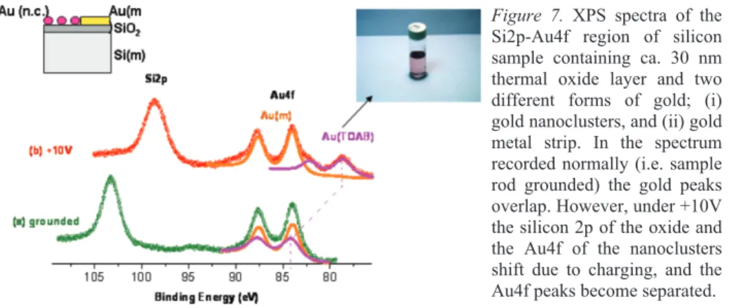
When the gold nanoparticles aggregate the solution becomes black and the absorption band shifts to longer wavelengths. A drop of solution containing the gold nanoclusters was deposited onto silicon substrates with various thermal oxide thicknesses (2-40 nm). The sample is tied onto the XPS sample holder together with a gold metal strip. Figure 7 depicts the Si2p-Au4f region recorded with and without external bias. An approximately 30 nm SiO2/Si substrate is chosen so that only the Si2p of the oxide is accessible by XPS.
Figure 7. XPS spectra of the
Si2p-Au4f region of silicon sample containing ca. 30 nm thermal oxide layer and two different forms of gold; (i) gold nanoclusters, and (ii) gold metal strip. In the spectrum recorded normally (i.e. sample rod grounded) the gold peaks overlap. However, under +10V the silicon 2p of the oxide and the Au4f of the nanoclusters shift due to charging, and the Au4f peaks become separated.
Our method is based on the ability to measure the local potential developed as a result of the different response of the gold metal and the 30 nm SiO2 dielectric layer to the external bias applied. As shown in Figure 7a, two peaks of the Au4f spin-orbit doublet from nanoclusters and the bulk gold overlap when the normal practice is employed. When the sample is biased at +10V (Figure 7b) the Si2p of the oxide shifts to lower binding energy, and the gold peaks separate into two doublets. One of the doublets does not shift but the other shifts almost as much as the Si2p peak. In this case the oxide is overneutralized by electrons from the filament, and has an overall negative potential which is also reflected in the Au4f of the nanoclusters.
By imposing a simple external voltage stress to the sample rod we have been able to control and measure the potential(s) developed as a result of charging in and on different layers/domains. This simple procedure is a powerful tool for enhancing peak separation.
4.2. DYNAMIC (PULSED) STIMULUS
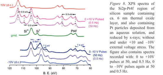
XPS analysis of a heterogeneous silicon sample with ca. 6 nm oxide layer, containing Pt particles deposited from an aqueous PtCl4 solution and reduced by
x-rays, is used to illustrate the pulsed technique. This involves x-ray induced production of Au nanoparticles on a SiO2/Si system and in polymer matrices.36 Pt behaves differently than gold on the SiO2/Si system and questions arise such as whether or not complete reduction is accomplished, or silicide formation has taken place, etc.
Figure 8 displays a series of XPS spectra of the Si2p-Pt4f region. The Si2p region consists of two peaks corresponding to the top oxide layer (Si4+) and the silicon substrate (Si0). The Pt4f region consists of one slightly broadened spin-orbit doublet, assigned to the formal oxidation state of Pt0 at 71.2 eV.1All the peaks shift after application of a d.c. voltage stress, but the shifts are different for the Si4+, Si0, and the Pt0 peaks due to variation of the differential charging.
Figure 8. XPS spectra of
the Si2p-Pt4f region of silicon sample containing ca. 6 nm thermal oxide layer, and also containing Pt particles deposited from an aqueous solution, and reduced by x-rays; without and under +10 and –10V external voltage stress. The figure also contains spectra recorded with: 0 to +10V pulses at 50, and 0.5 Hz, 0 to –10V pulses again at 50 and 0.5 Hz.
When the voltage stress is pulsed we observe both polarity and frequency dependent changes. For positive pulses all peaks are twinned with almost the same 9.9 eV energy difference, and almost no measurable frequency dependence. For negative pulses the measured energy difference between the twinned peaks varies and, more importantly, on the frequency of the voltage applied. As the voltage frequency decreases, the measured energy difference between the twinned peaks increase towards the asymptotic value of 9.9 eV. At low frequencies the measured binding energy difference between the twinned peaks increases since more time is allocated for equilibration.
The more important observation is that the measured difference between the twinned peaks of the Si4+, the Si0, and the Pt0 display different functional behavior with respect to frequency. The silicon oxide layer shifts the most, the silicon substrate in the middle, and the platinum species least. Measured binding energies can change several eV, depending on parameters like particle
size, matrix effects, and differential charging, etc.1,25,28,29,36 Tabulated binding energies for the Pt4f peak of the two silicides PtSi and Pt2Si are 73.0 and 72.5 eV, and are not very different from our observed value of 71.2 eV. However, on the basis of the frequency behavior of the peaks, silicide formation we can be ruled out, since otherwise both the Si0 and the Pt0 would shift together. Hence, we assign the observed Pt4f peak to separate metallic (probably nanometer size) particles on the oxide layer. Platinum’s behavior is different from gold, which displays a very tight shift with the oxide layer rather than with silicon. In the case of platinum the x-ray induced reduction is incomplete (unlike gold), and the particles contain some unreduced platinum species. The concentration of unreduced platinum is not high enough to be detected as a separate peak in the spectrum, but they are effective for charging the particles.
4.3. TIME-RESOLVED XPS
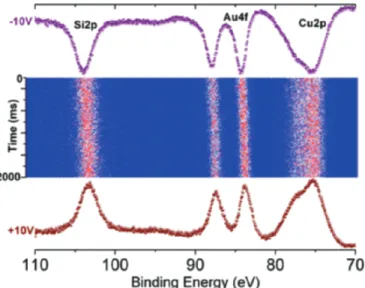
In Figure 9, 200 time resolved XPS spectra are shown. The nanoparticles have ca. 15 nm gold core and ca. 6 nm silica shell as determined by TEM.46 Both the Au4f and Si2p peaks shift to higher binding energies for the core-shell nanoparticles when recorded under –10V bias. Furthermore, their shifts are shift is solely related with charge accumulation in the silica shell, the extent of which can be controlled by the magnitude and the polarity of the voltage stress, and the gold core experiences the same potential, and shifts as the shell.
Figure 9. 200 time-resolved
XPS spectra recorded with 10 ms resolution of the Si2p-Au4f-Cu3p region of gold(core) /silica (shell) nanoparticles deposited on a copper tape.
We also examined Ag coated silica nanoparticles under exactly the same conditions. In this case, the Si2p shifts in a similar fashion, but the Ag3d peaks
exhibit no shift at all, since the silver atoms are now in the shell, and in contact with the copper substrate. Hence, it is possible to derive additional structural information from its charging behavior alone. Charging behavior of each peak enables us to detect and locate the charges chemically. Furthermore, from the measured shifts it is also possible to quantify the amount of charges stored on the nanoparticles.47
References
1. D. Briggs and M. P. Seah, Practical Surface Analysis. Part I. Auger and X-Ray Photoelectron Spectroscopy, Second edition (John Wiley & Sons Ltd., England, 1996).
2. T. L. Barr, Studies in Differential Charging, J. Vac. Sci. Technol. A 7, 1677-1683 (1989). 3. A. Cros, Charging Effects in X-Ray Photoelectron Spectroscopy, J. Electron Spectros. Relat.
Phenom. 59, 1-14 (1992).
4. T. Dickinson, A. F. Povey, and P. M. A. Sherwood, Differential Sample Charging in ESCA, J. Electron Spectros. Relat. Phenom. 2, 441-447 (1973).
5. G. Johansson, J. Hedman, A. Berndtsson, M. Klasson, and R. Nilsson, Calibration of Electron Spectra, J. Electron Spectros. Relat. Phenom. 2, 295-317 (1973).
6. J. Cazaux and P. Lehuede, Some Physical Descriptions of the Charging Effects of Insulators under Incident Particle Bombardment, J. Electron Spectros. Relat. Phenom. 59, 49-71 (1992). 7. J. Cazaux, Mechanisms of Charging in Electron Spectroscopy, J. Electron Spectros. Relat.
Phenom. 105, 155-185 (1999).
8. J. Cazaux, About the Charge Compensation of Insulating Samples in XPS, J. Electron Spectros. Relat. Phenom. 113, 15-33 (2000).
9. P. E. Larson, and M. A. Kelly, Surface Charge Neutralization of Insulating Samples in X-Ray Photoemission Spectroscopy, J. Vac. Sci. Technol. A 16, 3483-3489 (1998).
10. M. Marsi, R. Belkhou, C. Grupp, G. Panaccione, A. Taleb-Ibrahimi, L. Nahon, D. Garzella, D. Nutarelli, E. Renault, R. Roux, M. E. Couprie, and M. Billardon, Transient Charge Carrier Distribution at UV-Photoexcited SiO2/Si Interfaces, Phys. Rev. B 61, R5070-R5073 (2000).
11. J. Cazaux, Electron and X-Ray Induced Electron Emissions from Insulators, Polym. Int. 50, 748-755 (2001).
12. W. M. Lau, Use of Surface Charging in X-Ray Photoelectron Spectroscopic Studies of Ultrathin Dielectric Films on Semiconductors, Appl. Phys. Lett. 54, 338-340 (1989).
13. W. M. Lau, Effects of a Depth-Dependent Specimen Potential on X-Ray Photoelectron Spectroscopic Data, J. Appl. Phys. 65, 2047-2052 (1989).
14. W. M. Lau and X. W. Wu, Measurements of Interface State Density by X-Ray Photoelectron Spectroscopy, Surf. Sci. 245, 345-352 (1991).
15. R. W. M. Chan, R. W. M. Kwok, and W. M. Lau, Modified Surface Charge Spectroscopy for the Characterization of Insulator/Semiconductor Structures, J. Appl. Phys. 79, 3635-3639 (1996).
16. R. W. M. Chan, R. W. M. Kwok, W. M. Lau, H. Yan, and S. P. Wong, Studies of Electrical and Chemical Properties of SiO2/Si after Rapid Thermal Nitridation Using Surface Charge
Spectroscopy and X-Ray Photoelectron Spectroscopy, J. Vac. Sci. Technol. A 15, 2787-2792 (1997).
17. W. M. Lau, A Surface Charging Technique in Photoemission Spectroscopic Studies of Dielectric-Semiconductor Structures, J. Appl. Phys. 67, 1504-1509 (1990).
18. W. M. Lau, S. Jin, X.-W. Wu, and S. Ingrey, In Situ X-Ray Photoelectron Spectroscopic Study of Remote Plasma Enhanced Chemical Vapor Deposition of Silicon Nitride on Sulfide Passivated Inp, J. Vac. Sci. Technol. B 8, 848-855 (1990).
19. J. H. Thomas III, C. E. Bryson III, and T. R. Pampalone, X-Ray Photoelectron Spectroscopy Surface Charge Buildup Used to Study Residue in Deep Features on Integrated Circuits, J. Vac. Sci. Technol. B 6, 1081-1086 (1988).
20. A. Ermolieff, S. Deleonibus, S. Marthon, B. Blanchard, and J. Piaguet, Study of SiO2/Si
Interface States in Mos Devices by Surface Charge Spectroscopy. Application to Rapid Thermal Nitridation of Silicon, J. Electron Spectros. Relat. Phenom. 67, 409-416 (1994). 21. F. H. Bell and O. Joubert, Polysilicon Gate Etching in High Density Plasmas. 5. Comparison
between Quantitative Chemical Analysis of Photoresist and Oxide Masked Polysilicon Gates Etched in Hbr/Cl-2/O-2 Plasmas, J. Vac. Sci. Technol. B 15, 88-97 (1997).
22. J. D. Miller, W. C. Harris, and W. G. Zajac, Composite Interface Analysis Using Voltage Contrast Xps, Surf. Interface Anal. 20, 977-983 (1993).
23. H. Doron-Mor, A. Hatzor, A. Vaskevich, T. van der Boom-Moav, A. Shanzer, I. Rubinstein, and H. Cohen, Controlled Surface Charging as a Depth-Profiling Probe for Mesoscopic Layers, Nature 406, 382-385 (2000).
24. K. Shabtai, S. R. Cohen, H. Cohen, and I. Rubinstein, A Composite Gold-Silicon Oxide Surface for Mesoscopic Patterning, J. Phys. Chem. B 107, 5540-5546 (2003).
25. S. Suzer, Differential Charging in X-Ray Photoelectron Spectroscopy: A Nuisance or a Useful Tool? Anal. Chem. 75, 7026-7029 (2003).
26. G. Ertas and S. Suzer, XPS Analysis with External Bias: A Simple Method for Probing Differential Charging, Surf. Interface Anal. 36, 619-623 (2004).
27. N. J. Havercroft and P. M. A. Sherwood, Use of Differential Surface Charging to Separate Chemical Differences in X-Ray Photoelectron Spectroscopy, Surf. Interface Anal. 29, 232-240 (2000).
28. F. Karadas, G. Ertas, and S. Suzer, Differential Charging in SiO2/Si System as Determined by
XPS, J. Phys. Chem. B 108, 1515-1518 (2004).
29. B. Ulgut and S. Suzer, Xps Studies of SiO2/Si System under External Bias, J. Phys. Chem. B
107, 2939-2943 (2003).
30. B. V. Enüstün and T. Turkevich, Coagulation of Colloidal Gold, J. Am. Chem. Soc. 85, 3317-3328 (1963).
31. S. L. Cumberland and G. F. Strouse, Analysis of the Nature of Oxyanion Adsorption on Gold Nanomaterial Surfaces, Langmuir 18, 269-276 (2002).
32. S. Iwata and A. Ishizaka, Electron Spectroscopic Analysis of the SiO2/Si System and
Correlation with Metal-Oxide-Semiconductor Device Characteristics, J. Appl. Phys. 79, 6653-6713 (1996).
33. A. Ishizaka, S. Iwata, and Y. Kamigaki, Si-SiO2 Interface Characterization by ESCA, Surf.
Sci. 84, 235-537 (1979).
34. K. Luo, D. Y. Kim, and D. W. Goodman, The Nucleation and Growth of Gold on Silica, J. Mol. Catal. A 167, 191-198 (2001).
35. M. G. Mason, Electronic Structure of Supported Small Metal Clusters, Phys. Rev. B 27, 749-762 (1983).
36. F. Karadas, G. Ertas, E. Ozkaraoglu, and S. Suzer, X-Ray-Induced Production of Gold Nanoparticles on a SiO2/Si System and in a Poly(Methyl Methacrylate) Matrix, Langmuir 21,
437-442 (2005).
37. G. Ertas, U. K. Demirok, and S. Suzer, Enhanced Peak Separation in XPS with External Biasing, Appl. Surf. Sci. 249, 12-15 (2005).
38. C. Battistoni, G. Mattogno, and D. M. P. Mingos, Characterization of Some Gold Cluster Compounds by X-Ray Photoelectron Spectroscopy, J. Electron Spectros. Relat. Phenom. 33, 107-113 (1984).
39. C. Battistoni, G. Mattogno, and D. M. P. Mingos, Characterisation of Some Gold Clusters by X-Ray Photoelectron Spectroscopy, J. Electron Spectros. Relat. Phenom. 28, 23-31 (1982). 40. A. Howard, D. N. S. Clark, C. E. J. Mitchell, R. G. Egdell, and V. R. Dhanak, Initial and
Final State Effects in Photoemission from Au Nanoclusters on TiO2(110), Surf. Sci. 518,
210-224 (2002).
41. T. Ohgi, H. Y. Sheng, Z. C. Dong, H. Nejoh, and D. Fujita, Charging Effects in Gold Nanoclusters Grown on Octanedithiol Layers, Appl. Phys. Lett. 79, 2453-2455 (2001). 42. T. Ohgi and D. Fujita, Consistent Size Dependency of Core-Level Binding Energy Shifts and
Single-Electron Tunneling Effects in Supported Gold Nanoclusters, Phys. Rev. B 66, 115410-115415 (2002).
43. M. Brust, M. Walker, D. Bethell, D. J. Schiffrin, and R. Whyman, Synthesis of Thiol-Derivatized Gold Nanoparticles in a 2-Phase Liquid-Liquid System, J. Chem. Soc. Chem. Commun. 7, 801-802 (1994).
44. A. N. Shipway, M. Lahav, R. Gabai, and I. Willner, Investigations into the Electrostatically Induced Aggregation of Au Nanoparticles, Langmuir 16, 8789-8795 (2000).
45. M. M. Alvarez, J. T. Khoury, T. G. Schaaff, M. N. Shafigullin, I. Vezmar, and R. L. Whetten, Optical Absorption Spectra of Nanocrystal Gold Molecules, J. Phys. Chem. B 101, 3706-3712 (1997).
46. I. Tunc, S. Suzer, M. A. Correa-Duarte, L. M. Liz-Marzan, XPS Characterization of Au (Core)/SiO2 (Shell) Nanoparticles J. Phys. Chem. B 109, 7597-7600 (2005).
47. I. Tunc, S. Suzer, M. A. Correa-Duarte, and L. M. Liz-Marzan, Charging/Discharging of Au (Core)/Silica (Shell) Nanoparticles as revealed by XPS, J. Phys. Chem. B (to be published).