Summary. We experimentally and theoretically demonstrate negative refraction and focusing on electromagnetic (EM) waves by using two-dimensional photonic crystal slabs at microwave frequencies. Negative refraction is observed both for transverse magnetic (TM) and transverse electric (TE) polarized incident EM waves. Gaussian beam shifting method is used to verify negative refractive index. Subwave-length imaging and flat lens behavior of photonic crystals are successfully demon-strated. We have been able to overcome the diffraction limit and focus the EM waves to a spot size of 0.21λ. Metallodielectric photonic crystals are employed to increase the range of angles of incidence that results in negative refraction. Experimental results and theoretical calculations are in good agreement throughout the work.
6.1 Introduction
Materials which possess negative index of refraction have become a remarkable research area in recent years [1–10]. One approach taken is to construct a com-posite metamaterial [2–5] consisting of two components which have a negative permittivity [11] (ε(ω) < 0) and negative permeability [12] (µ(ω) < 0) simul-taneously over a certain frequency range, respectively, so that the resulting index of refraction of the effective medium becomes neff =
√
ε√µ < 0 [6–10].
Such structures are able to behave like a perfect lens, where both the propa-gating and evanescent waves contribute to the focusing [13]. Another path is revealed by the photonic crystals (PCs), where the band structure can lead to negative dispersion for electromagnetic (EM) waves.
Photonic crystals are periodic dielectric or metallic structures that have photonic bands exhibiting arbitrarily different dispersions for the propaga-tion of EM waves, and band gaps, where the propagapropaga-tion is prohibited at certain range of wavelengths [14–18]. In this respect, there is a close analogy between a photon in a photonic crystal, and an electron in a semiconduc-tor. Based on these properties, photonic crystals provide a medium where the propagation of light can be modified virtually in any way in a controllable
[39, 40]. Subwavelength imaging and resolution [41] and flat lens behavior [42] of PCs have been experimentally demonstrated. Extensive numerical [43–46] and experimental studies [47–52] helped to have a better understanding of negative refraction, focusing, and subwavelength imaging in photonic crystal structures.
In this chapter, we review certain recent studies on the negative refrac-tion and imaging of EM waves by photonic crystal slabs in the microwave frequency regime. We first report on the negative refraction and the sub-wavelength imaging with transverse magnetic (TM) polarized EM waves. Then we show that it is also possible to have negative refraction with trans-verse electric (TE) polarized EM waves. Fifth band of the photonic crystal is utilized for purpose of achieving negative refraction. A spectral negative refraction and focusing behavior will be provided. Finally we demonstrate a metallodielectric PC that possesses negative refraction and imaging through a slab. Throughout the work two basic mechanisms arising from the band structure of PCs are employed to obtain negative refraction. We found that focusing abilities of a PC slab can surpass that of conventional (i.e., positive refractive) materials, providing both subwavelength imaging and true flat lens behavior.
6.2 Negative Refraction and Subwavelength Imaging
of TM Polarized Electromagnetic Waves
Refraction is perhaps one of the most basic topics of electromagnetic phenom-ena, whereby when a beam of radiation is incident on an interface between two media at an arbitrary angle, the direction of propagation of the transmitted beam is altered by an amount related to the indices of refraction of the two media. Although all of the known naturally occurring materials exhibit posi-tive indices of refraction, the possibility of materials with negaposi-tive refracposi-tive index has been explored theoretically by Victor Veselago [1]. In his semi-nal work, he concluded that such materials did not violate any fundamental physical laws. These materials were termed left-handed materials (LHMs),
ε = 9.61, radius r = 1.6 mm, and length l = 150 mm [36]. The periodicity of
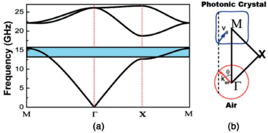
the structure in both directions is a = 4.79 mm. The analysis of Luo et al [34] is followed to determine the negative refraction frequency range of our struc-ture, which is calculated to be 13.10–15.44 GHz. Propagation properties of the EM wave within the crystal can be described by studying equal-frequency contours (EFCs) in k-space. The TM polarized band diagram of the photonic crystal calculated by plane wave expansion method is shown in Fig. 6.1a. We focus on the first band for the experimental and theoretical demonstration of single-beam negative refraction in 2D photonic crystals. EFCs of the photonic crystal and air at 13.698 GHz are schematically drawn in Fig. 6.1b. The conser-vation of the surface-parallel wave vector gives the direction of the refracted waves inside the PC [34]. The negative refraction effect is present at this frequency.
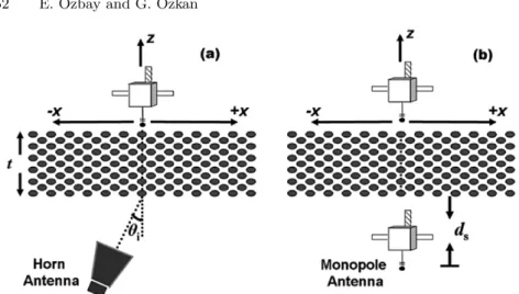
The refraction spectrum is measured by a setup consisting of an HP 8510C network analyzer, a standard high-gain microwave horn antenna as the transmitter, and a monopole antenna as the receiver (Fig. 6.2a). The size of the monopole antenna is 11 mm, which is half of the operation wavelength
Fig. 6.1. (a) Calculated band diagram of 2D photonic crystal for transverse mag-netic (TM) polarization. (b) Equal-frequency contours in k-space of PC and air at 13.698 GHz. θ is the incident angle and vg is the group velocity inside the PC
Fig. 6.2. Schematic drawing of the experimental setup for observing (a) negative refraction phenomenon, (b) focusing effect of a slab of negative refractive 2D PC
(λ∼ 22 mm) of the EM wave at a working frequency of f = 13.698 GHz. The top view of the experimental setup is given in Fig. 6.2a. The x and z direc-tions are shown in the figure, whereas the y is directed out of the page. The electric field is along the y-direction (i.e., parallel to the rods), whereas the magnetic field and wave-vector are on the x–z plane. The horn antenna is oriented such that the incident waves make an angle of 45◦ with the normal of Γ –M interface.
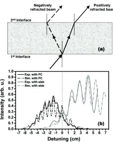
The spatial distributions of the time-averaged incident field intensity along the second (PC–air) interface are measured (Fig. 6.3a). The PC used in nega-tive refraction experiments has 17 layers along the propagation direction (z) and 21 layers along the lateral direction (x). For a direct comparison of theo-retical predictions and experimental results, simulation of the structure based on experimental parameters using a finite difference time domain (FDTD) method is performed. The incident EM wave has a Gaussian beam profile centered at x = 0. Therefore, by measuring the shift of the outgoing beam as given in Fig. 6.3a, one can easily deduce whether the structure has a positive or negative refractive index.
Figure 6.3b plots the measured (solid) and simulated (dashed-dotted) spa-tial distributions of intensity at the interfaces for the slabs of PC (black) and randomly filled polystyrene pellets (gray). As clearly seen in Fig. 6.3b, the cen-ter of the outgoing Gaussian beam is shifted to the left side of the cencen-ter of the incident Gaussian beam for the PC structure. Due to Snell’s law, this behavior corresponds to negative refraction. Experimental results and numerical sim-ulations agree well. Refractive index of PC at 13.698 GHz determined from the experiment is−1.94, which is very close to the theoretical value of −2.06 computed by the FDTD method. For comparison purposes, the measurements and the simulations are repeated with a slab that contains only polystyrene
Fig. 6.3. (a) Schematics of refraction of the incident beam through positive and neg-ative media for TM polarization. (b) Refraction spectrum of incident beam through negative refractive PC (black lines) and positive refractive polystyrene pallets (gray lines). The solid lines and the dashed-dotted lines correspond to the experimental measurements and theoretical simulations, respectively
pellets, which has a positive refractive index (n=1.46). The refracted beam emerges from the right-hand side of the incident beam as plotted in Fig. 6.3b. The positive refractive index determined from the experiment is 1.52, which is close to the tabulated value of 1.46.
A negative refractive index allows a flat lens to bring EM waves into focus, whereas positive refractive index materials always require curved surfaces to focus EM waves [1, 13]. One interesting physical behavior of negative index materials is that they can restore the amplitude of evanescent waves and therefore enable subwavelength focusing [13, 43]. Subwavelength resolution was experimentally verified for negative index materials made of PCs [36]. To investigate the focusing ability of the present PC, a slab of the same PC (with 15×21 layers) is employed. The operation frequency is set to 13.698 GHz, hav-ing the largest angular range for negative refraction [36]. FDTD simulations
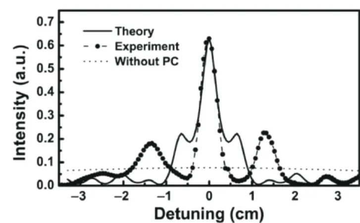
Fig. 6.4. Measured power distribution (large dotted-dashed line) and calculated average intensity (solid line) at the focal point for TM polarization. Dashed line is the spatial power distribution without PC
with experimental parameters predict the formation of an image 0.7 mm away from the PC–air interface for a point source that is placed 0.7 mm away from the air–PC interface. We first simulated the distribution of time-averaged intensity along the PC–air interface with and without the PC (solid curve and thin dotted curve in Fig. 6.4). In the experiment, a monopole antenna is used as the point source (Fig. 6.2b). The measured (large dotted-dashed) and calculated (solid) power distribution along the interface is depicted in Fig. 6.4. The full width at half maximum (FWHM) of the measured focused beam is found to be 0.21λ, which is in good agreement with the calculated FWHM. In contrast, the calculated FWHM of the beam at this plane in the absence of the PC is found to be 5.94λ (dashed line in Fig. 6.4). This implies an enhancement of the transmitted field about 25 times compared to that of free space.
6.3 Negative Refraction and Point Focusing
of TE Polarized Electromagnetic Waves
In Sect. 6.2 the negative refraction originating from the convex EFCs of the first band around the M -point in k-space was investigated. The first band has a partial gap around Γ -point, and the EM waves are forced to move along the Γ –M -direction, where the conservation of the surface-parallel component of the wave vector causes negative refraction (Fig. 6.1a). In this section, we employ a different band topology of a 2D PC to obtain negative refraction [47]. We aim to achieve negative refractive index with higher isotropy. Based on the analysis presented in [45], we utilize a TE polarized upper band of the PC where the magnetic field is parallel to the dielectric rods. A similar study using the TM polarized band was recently reported by Martinez et al. [49]
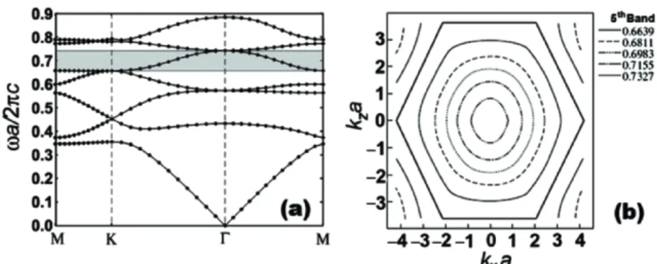
Fig. 6.5. (a) Calculated TE polarized band structure. Shaded band (fifth band) covers the frequencies where the structure possesses negative index of refraction. (b) Equal-frequency contours of the fifth band in the full Brillouin zone. The contours are nearly circular (i.e., isotropic) and shrink with increasing frequency
We used the same photonic crystal structure as analyzed in Sect. 6.2. The only difference is that we calculated the band diagram for TE polarized EM waves. Figure 6.5a depicts the calculated band diagram in the first Brillouin zone. The transverse direction is taken to be in the plane of 2D PC. We scaled frequency withf = f (a/c). The fifth band as shaded in the Fig. 6.5a extends∼
from ∼f = 0.65(f = 40.65 GHz) to ∼f = 0.74(f = 46.27 GHz). Figure 6.5b
plots the EFCs in the full Brillouin zone. The EFCs of the band shrink with increasing frequency, contrary to the EFCs in air (n = 1).
The refraction spectra are measured by using same setup as in Fig. 6.2a. Since the EM wave is TE polarized in this case, the horn and the monopole antennas are rotated by 90◦. Therefore the magnetic field is parallel to the dielectric rods. The PC structure consists of seven layers along the propa-gation direction (z) and 31 layers along the lateral direction (x). The horn antenna is on the negative side of the PC with respect to its central axis. The scanning is performed along the second PC–air interface by ∆x = 1.27 mm steps. Refraction spectra of the EM waves with three different incident angles are measured and the results are plotted in Fig. 6.6. The top part of Fig. 6.6 gives the field distribution along the PC–air interface as a function of fre-quency. It is evident that the refracted beam appears (for θi=15◦ (a), θi=30◦
(b), and θi=45◦ (c)) on the negative side, meaning that the PC structure has
negative refractive index between 40.0 and 43.0 GHz.
When the incidence angle is increased, the transmission shifts to the left accordingly. To investigate the beam profiles, the spatial cross-sections at
f =41.7 GHz are plotted in the middle part of Fig. 6.6. The intensities are
nor-malized with respect to the maximum intensity for the incident angle θi = 15◦.
It is apparent that the lateral shift is accompanied by a decrease in the trans-mission intensity. This is due to the higher reflection at the interface for larger incidence angles and the diffraction-induced out-of-plane losses, which increase
Fig. 6.6. Measured refraction spectra of the fifth band along the PC–air interface for incidence angles of (a) θi=15◦, (b) θi=30◦, and (c) θi=45◦ is given on the top
figures. Middle figures are the measured, whereas the bottom figures are the sim-ulated intensity profiles at 41.7 GHz for the respective angles of incidence. Solid curves indicate the Gaussian fits of the data. All results are for TE polarization with increasing path length through the lattice. The bottom part of Fig. 6.6 displays the simulated average field intensity at f =41.7 GHz. Experimental results agree well with the FDTD simulations. By using Snell’s law, index of refraction is obtained to be neff =−0.52, −0.66, and −0.86 from the
exper-iment for θi= 15◦, 30◦, and 45◦, respectively. The simulation results for the
same incidence angles give neff =−0.66, −0.72, and −0.80. The experimental
and theoretical results agree quite well. We observed that the band manages to provide a negative refracted uniform beam within the measured frequency range both from the experiments and simulations.
We have also checked the imaging properties of our PC slab for TE polar-ized EM waves. FDTD simulations are performed at f =42.07 GHz located at a distance ds= 2λ away from air–PC interface. Omnidirectional (point) source
is used to excite the first interface. Figure 6.7a displays the resulting spatial intensity distribution in the image plane, normalized to the value of maximum intensity. The PC–air interface is located at z = 0. The peak indicates focus-ing behavior unambiguously. We would like to emphasize that the focusfocus-ing
Fig. 6.7. (a) Simulated 2D intensity profile in the image plane. z=0 corresponds to the PC–air interface. (b) Measured lateral intensity profiles along the propagation direction. Measurements are performed at six different positions z/λ = 1.78, 3.56, 5.34, 7.12, 8.90, and 10.68 for TE polarization
occurs away from the PC–air interface, observed at z≈ 8λ. Therefore, unlike the focusing discussed in Sect. 6.2 for TM polarized EM wave, this PC does not perform imaging in the strict sense. Also a subwavelength imaging as pre-sented in Fig. 6.4 is not present since the focal point is quite far away from the interface.
Experimental setup for verifying focusing through a slab of PC is similar to the one discussed in Sect. 6.2 (Fig. 6.2b). But to imitate a TE polarized monopole antenna, we employed a waveguide aperture as the source. The waveguide aperture provides sufficiently omnidirectional radiation due to the diffraction at the aperture [47]. The intensity distribution in the focusing plane is measured by the monopole antenna. For ds= 2λ, first a scan is performed
along the propagation direction (z) to locate the maximum intensity, i.e., the focal point. Then, lateral cross-sections (along x) of field intensity at several z points around the peak position are measured. As seen in Fig. 6.7b, the beam is focused both in lateral and longitudinal directions. The maximum intensity is observed at z≈ 8λ, the focal point. The longitudinal extent of the focusing indicates that index of refraction deviates from negative unity, and bears a certain amount of anisotropy. We stress that even when refractive indices were perfectly isotropic and uniform, a value different from n =−1 would not generate point focusing and would induce an aberration of the image.
6.4 Negative Refraction and Focusing Analysis
for a Metallodielectric Photonic Crystal
In Sects. 6.2 and 6.3 we have dealt with dielectric photonic crystals. Photonic crystal structures can also be made of metals. But it is not easy to obtain neg-ative refraction from the metallic photonic crystal structures since the EFCs
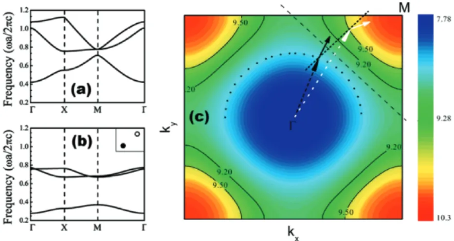
attractive perturbation and causes lowering the frequency of the bands [50]. The metallodielectric photonic crystal is a square lattice of metallic and dielectric rods where the basis of the PC consists of a metallic and a dielectric rod placed along the diagonal of the square unit cell as given in the inset of Fig. 6.8b. Cylindrical alumina rods with a radius of 1.55 mm are used as the dielectric rods with ε = 9.61. The metallic rods are made of aluminum and have a radius of 1.5 mm. Both the metallic and dielectric rods have a height of 150 mm.
We have computed the band diagrams of the metallic photonic crystal (Fig. 6.8a) and metallodielectric photonic crystal (Fig. 6.8b) for TM polar-ized EM waves. The radius of the dielectric rod is 0.136a, and the radius
Fig. 6.8. (a) Calculated TM-polarized bands for the metallic photonic crystal, and (b) the metallodielectric crystal. (c) Equal-frequency contours (solid curves) are shown for the metallodielectric PC. Dotted circle is the free-space equal-frequency contour at 9.5 GHz. Free-space wave vector (black dashed arrow ), free-space group velocity (black solid arrow ), wave vector of the refracted waves in the PC (white dashed arrow ), group velocity inside the PC (white solid arrow ) are drawn
easily be obtained, as given in the figure. The group velocity of the incident waves and the group velocity of the transmitted waves fall on opposite sides of the surface normal. Therefore the incident waves are negatively refracted [34]. For the plotted EFCs, the magnitude of the largest surface-parallel wave vector component in air is smaller than the largest surface-parallel wave vector component in the photonic crystal. The range of incidence angles that are negatively refracted can be increased by lowering the bands without modifying the lattice parameters [50].
The electric field intensities are measured along the PC–air interface to demonstrate the negative refraction experimentally. The measurement method is same with the measurements indicated in the previous sections (Fig. 6.2a). Waves that are positively refracted are expected to emerge from the positive side of the surface, whereas negatively refracted waves are to emerge from the negative side. Measurement results for incidence angles of θi=15◦, 25◦, 35◦,
and 45◦ are provided in Fig. 6.9a–d, respectively. Between the frequencies 9.20 and 10.30 GHz waves exit from the negative side of the PC meaning that EM waves are negatively refracted by the PC in this frequency range. Up to 9.20 GHz the waves are positively refracted.
We have also performed FDTD simulations to see how the EM wave is refracted by the metallodielectric PC. We have sent an incident Gaussian beam to the air–PC interface and calculated electric field intensities inside and outside the PC at 9.70 GHz. The simulation results for two different inci-dent angles θi=15◦ (Fig. 6.10a) and θi=45◦ (Fig. 6.10b) clearly show that the
negative refraction takes place at this frequency. The effect of reflection is also clear in this picture. For higher incident angle the intensity (therefore the transmission) is lower due to the high reflections from the air–PC interface. Note that 9.70 GHz is in the negative refraction frequency regime as calculated from the EFCs (Fig. 6.8c).
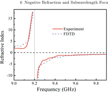
We have compared the experimental and theoretical results of the val-ues of refractive indices at θi=25◦ incidence angle in Fig. 6.11. Between
9.00 and 9.19 GHz the refractive indices are found to be positive. Around 9.20 GHz there is an abrupt change in the values and the sign of the index of refraction. In the close vicinity of 9.20 GHz the indices of refraction are found to be high, +18 and −12 due to the flatness of EFS contours around 9.20 GHz (Fig. 6.8c). The refractive indices are negative in the frequency range
Fig. 6.9. Measured electric field intensities along the PC–air interface for incident angles of (a) θ=15◦, (b) θ=25◦, (c) θ=35◦, and (d) θ=45◦for the metallodielectric PC. The intensities are plotted as a function of frequency. Up to 9.2 GHz the struc-ture is positively refracting and between 9.2 and 10.3 GHz the strucstruc-ture refracts negatively
Fig. 6.10. Simulated electric field distributions for both angles of incidence. Incident angles of (a) θ=15◦and (b) θ=45◦for the metallodielectric PC. Negative refraction phenomenon is clearly observed for both angles of incidence
9.25–10.00 GHz. As seen in Fig. 6.11 the refractive indices depend strongly on the frequency. This is an expected behavior since the EFCs (Fig. 6.8c) are anisotropic throughout the frequency range of interest. Measured refractive index values are−0.65, −0.85, −0.88, and −0.96 for four different incidence
Fig. 6.11. Measured (solid line) and calculated (dashed line) refractive indices at an angle of incidence 15◦for the metallodielectric PC
Fig. 6.12. Spatial intensity distribution of an outgoing EM wave at 3.70 GHz along the x–z plane of the metallodielectric PC. The wave is refracted negatively since the beam emerges from the negative side of the normal
angles of 15◦, 25◦, 35◦, and 45◦, respectively, at 9.70 GHz. These results clearly show that refractive index also depends on the incidence angle. To obtain uni-form angle-independent negative indices of refraction two conditions must be satisfied. First, a circular EFC centered at the origin of the Brillouin zone is required. Second, the radius of the circular EFC must be decreasing with increasing frequency [50].
We have also scanned the intensity distribution of the EM wave by a mono-pole antenna mounted to a 2D scanning table with ∆x = ∆z = 2.5 mm steps. In our experiments we can only measure the power at a certain point, which corresponds to the time-averaged intensity at that point. Note that up to this point we have only scanned the field along PC–air interface for measuring the index of refraction. The resulting scanned field profile at 9.70 GHz is plotted in Fig. 6.12. We can clearly see how the wave propagates after being refracted
from the PC–air interface. The intensities are normalized with respect to the maximum intensity. The incident EM wave has a Gaussian beam profile cen-tered at x = 0. Gaussian beam is shifted by 40 mm to the negative side of the normal as expected from a negatively refracting medium.
A similar field scan is performed for the observation of focusing through a PC slab lens. In this case we have used a monopole antenna as a point source to shine the air–PC interface (refer to Fig. 6.2b for setup). EM waves emerging from a point source located near a lens with negative refractive index will first be refracted through the first air–PC interface and will come into focus inside the PC. Then outgoing EM waves will face refraction again at the second PC–air interface and the refracted beam will meet the optical axis of flat lens, where the second focusing will occur. If the lens is not thick enough, the focusing may not occur inside the lens, which in turn will result in a diverging beam instead of a converging beam, even if the material is negatively refracting. Therefore, the thickness of the lens plays a crucial role for observing flat lens behavior.
Figure 6.13 provides the transmission spectrum for the omnidirectional source located at ds= 7 cm away from the PC lens. Number of layers along
the propagation direction is Nz = 10. As seen in Fig. 6.13, an image is formed
at a focal length of z = 4 cm. Focusing is obtained both in the lateral and the propagation direction. If the slab was made of a positive refractive material, it would not be possible to observe a point focusing. For such positive refractive index slab lenses the beam will diverge as expected from ray optics. Therefore flat lens focusing is available only for negative refractive media.
6.5 Conclusion
In this chapter, the negative refraction and the focusing abilities of 2D dielec-tric and metallodielecdielec-tric photonic crystals were investigated both experimen-tally and theoretically. We have observed that an effective index of refraction
ing band diagram is calculated and a lowering in frequency of the bands is observed.
The advantage of using photonic crystals as negative refractive media is that the transmission is higher compared to lossy LHM. Also the electromag-netic phenomena discussed here depend only on the refractive index of the dielectric material and on the geometrical parameters of the 2D PC, hence it is scalable across the electromagnetic spectrum. With advancing fabrica-tion techniques, photonic crystals are now seen as essential building blocks of applications in the infrared and optical frequencies. It is much more difficult to scale the LHM that are made of metallic structures.
Acknowledgments
This work is supported by the European Union under the projects EU-DALHM, EU-NOE-METAMORPHOSE, EU-NOE-PHOREMOST, and TUBITAK under Project No. 104E090. Ekmel Ozbay acknowledges partial support from the Turkish Academy of Sciences.
References
1. V.G. Veselago, Sov. Phys. Usp. 10, 504 (1968)
2. D.R. Smith, W.J. Padilla, D.C. Vier, S.C. Nemat-Nasser, S. Schultz, Phys. Rev. Lett. 84, 4184 (2000)
3. R.A. Shelby, D.R. Smith, S.C. Nemat-Nasser, S. Schultz, Appl. Phys. Lett. 78, 489 (2001)
4. M. Bayindir, K. Aydin, P. Markos, C.M. Soukoulis, E. Ozbay, Appl. Phys. Lett. 81, 120 (2002)
5. K. Aydin, K. Guven, M. Kafesaki, L. Zhang, C.M. Soukoulis, E. Ozbay, Opt. Lett. 29, 2623 (2004)
6. R.A. Shelby, D.R. Smith, S. Schultz, Science 292, 77 (2001)
7. C.G. Parazzoli, R.B. Greegor, K. Li, B.E. Koltenbah, M. Tanielian, Phys. Rev. Lett. 90, 107401 (2003)
8. A.A. Houck, J.B. Brock, I.L. Chuang, Phys. Rev. Lett. 90, 137401 (2003) 9. K. Aydin, K. Guven, C.M. Soukoulis, E. Ozbay, Appl. Phys. Lett. 86, 124102
New York, 2001)
19. E. Ozbay, G. Tuttle, R. Biswas, K.M. Ho, J. Bostak, D.M. Bloom, Appl. Phys. Lett. 65, 1617 (1994)
20. E. Ozbay, B. Temelkuran, Appl. Phys. Lett. 69, 743 (1996)
21. A. Mekis, J.C. Chen, I. Kurland, S. Fan, P.R. Villeneuve, and J.D. Joannapoulos, Phys. Rev. Lett. 77, 3787 (1996)
22. P.R. Villeneuve, D.S. Abrams, S. Fan, J.D. Joannopoulos, Opt. Lett. 21, 2017 (1996)
23. B. Temelkuran, E. Ozbay, J.P. Kavanaugh, G. Tuttle, K.M. Ho, Appl. Phys. Lett. 72, 2376 (1998)
24. H. Kosaka, T. Kawashima, A. Tomita, M. Notomi, T. Tamamura, T. Sato, S. Kawakamib, Appl. Phys. Lett. 74, 1370 (1999)
25. M. Bayindir, E. Ozbay, Phys Rev. B 62, R2247 (2000)
26. M. Loncar, D. Nedeljkovic, T. Doll, J. Vuckovic, A. Scherer, T.P. Pearsall, Appl. Phys. Lett. 77, 1937 (2000)
27. S. Noda, M. Yokoyama, M. Imada, A. Chutinan, M. Mochizuki, Science 293, 1123 (2001)
28. M. Bayindir, S. Tanriseven, E. Ozbay, Appl. Phys. A-Mater. Sci. Process. 72, 117 (2001)
29. E. Ozbay, M. Bayindir, I. Bulu, E. Cubukcu, IEEE J. Quantum Electron. 38, 837 (2002)
30. S. Enoch, B. Gralak, G. Tayeb, Appl. Phys. Lett. 81, 1588 (2002) 31. M.F. Yanik, S. Fan, Phys. Rev. Lett. 92, 083901 (2004)
32. B. Gralak, S. Enoch, G. Tayeb, J. Opt. Soc. Am. A 17, 1012 (2000) 33. M. Notomi, Phys. Rev. B 62, 10696 (2000)
34. C. Luo, S.G. Johnson, J.D. Joannopoulos, J.B. Pendry, Phys. Rev. B 65, 201104 (2002)
35. S. Foteinopoulou, E.N. Economou, C.M. Soukoulis, Phys. Rev. Lett. 90, 107402 (2003)
36. E. Cubukcu, K. Aydin, E. Ozbay, S. Foteinopoulou, C.M. Soukoulis, Nature 423, 604 (2003)
37. P.V. Parimi, W.T. Lu, P. Vodo, J. Sokoloff, J.S. Derov, S. Sridhar, Phys. Rev. Lett. 92, 127401 (2004)
38. A. Berrier, M. Mulot, M. Swillo, M. Qiu, L. Thyl´en, A. Talneau, S. Anand, Phys. Rev. Lett. 93, 073902 (2004)
39. H. Kosaka, T. Kawashima, A. Tomita, M. Notomi, T. Tamamura, T. Sato, S. Kawakami, Phys. Rev. B 58, R10096 (1998)
47. K. Guven, K. Aydin, K.B. Alici, C.M. Soukoulis, E. Ozbay, Phys. Rev. B 70, 205125 (2004)
48. E. Ozbay, K. Guven, E. Cubukcu, K. Aydin, B.K. Alici, Mod. Phys. Lett. B 18, 1275 (2004)
49. A. Mart´ınez, H. M´ıguez, A. Griol, J. Mart´ı, Phys. Rev. B 69, 165119 (2004) 50. I. Bulu, H. Caglayan, E. Ozbay, Phys. Rev. B 72, 045125 (2005)
51. P. Vodo, P.V. Parimi, W.T. Lu, S. Sridhar, R. Wing, Appl. Phys. Lett. 85, 1858 (2005)