• Sonuç bulunamadı

Low-temperature hollow cathode plasma-assisted atomic layer deposition of crystalline III-nitride thin films and nanostructures

N/A
N/A
Protected

Academic year: 2021

Share "Low-temperature hollow cathode plasma-assisted atomic layer deposition of crystalline III-nitride thin films and nanostructures"

Copied!
5
0
0

Yükleniyor.... (view fulltext now)

Tam metin

(1)

p s s

current topics in solid state physics

status

solidi

www.pss-c.com

physica

Low-temperature hollow cathode

plasma-assisted atomic layer deposition

of crystalline III-nitride thin films

and nanostructures

Cagla Ozgit-Akgun*,1,2, Eda Goldenberg2, Sami Bolat2,3, Burak Tekcan2,3, Fatma Kayaci1,2, Tamer Uyar1,2, Ali Kemal Okyay1,2,3, and Necmi Biyikli**,1,2

1 Institute of Materials Science and Nanotechnology, Bilkent University, Bilkent 06800 Ankara, Turkey 2 UNAM – National Nanotechnology Research Center, Bilkent University, Bilkent 06800 Ankara, Turkey 3 Department of Electrical and Electronics Engineering, Bilkent University, Bilkent 06800 Ankara, Turkey

Received 9 July 2014, revised 24 October 2014, accepted 20 January 2015 Published online 16 March 2015

Keywords AlN, GaN, InN, atomic layer deposition (ALD), hollow cathode plasma

** Corresponding author: e-mail ozgit@bilkent.edu.tr, Phone: +90 312 290 3551, Fax: +90 312 266 4365

** e-mail biyikli@unam.bilkent.edu.tr, Phone: +90 312 290 3556, Fax: +90 312 266 4365

Hollow cathode plasma-assisted atomic layer deposition (HCPA-ALD) is a promising technique for obtaining III-nitride thin films with low impurity concentrations at low temperatures. Here we report our previous and current ef-forts on the development of HCPA-ALD processes for III-nitrides together with the properties of resulting thin

films and nanostructures. The content further includes nylon 6,6-GaN core-shell nanofibers, proof-of-concept thin film transistors and UV photodetectors fabricated us-ing HCPA-ALD-grown GaN layers, as well as InN thin films deposited by HCPA-ALD using cyclopentadienyl indium and trimethylindium precursors.

© 2015 WILEY-VCH Verlag GmbH & Co. KGaA, Weinheim

1 Introduction Atomic layer deposition (ALD) is a cyclic, low-temperature thin film deposition method, in which the substrate surface is exposed to sequential pulses of two or more precursors separated by evacuation and/or purging periods. When compared to other deposition tech-niques, ALD stands out with its self-limiting growth mech-anism, which enables the deposition of highly uniform and conformal thin films with sub-angstrom thickness control. Layer-by-layer growth offered by ALD further enables the deposition of alloy thin films with well-defined composi-tions. These features make ALD a promising technique for the low-temperature deposition of III-nitrides and their al-loys on temperature-sensitive device layers and substrates, as well as on high surface area nanostructured templates for the synthesis of III-nitride nanostructures.

Although thermal ALD (or atomic layer epitaxy, ALE) of III-nitride thin films, especially AlN, using various types of group-III precursors has been the focus of interest in the 1990s, current trend in the field of III-nitride ALD research is directed towards UV-, hot-wire- or

plasma-assisted processes using metalorganic precursors [1-11]. Recently, we showed that ALD-grown III-nitride thin films may suffer from plasma-related oxygen contamination de-pending on the choice of N-containing plasma gas (N2,

N2/H2 or NH3) [12, 13]. Therefore, as an attempt to grow

O-free III-nitride thin films, we integrated an all stainless steel hollow cathode plasma (HCP) source to the ALD sys-tem, and thereby demonstrated the hollow cathode PA-ALD (HCPA-PA-ALD) of wurtzite AIN, GaN and AlxGa1-xN

thin films with low impurity concentrations at 200 °C [14]. GaN had not been deposited in a self-limiting fashion at such low temperatures since Sumakeris et al. [15] reported the growth of GaN using a novel reactor design employing hot filaments to decompose NH3 in 1993.

In this paper, we review our previous and current ef-forts on the development of HCPA-ALD processes for III-nitrides together with the properties of resulting thin films and nanostructures. The content further includes nylon 6,6-GaN core-shell nanofibers, proof-of-concept thin film tran-sistors (TFTs) and UV photodetectors fabricated using

(2)

(CpIn) and trimethylindium (InMe3) precursors.

2 Experimental details

2.1 Hollow cathode plasma-assisted atomic layer deposition AlN, GaN, AlxGa1-xN, and InN thin

films were deposited at 200 °C in a Fiji F200-LL ALD re-actor (Ultratech/Cambridge NanoTech Inc.) equipped with a stainless steel HCP source (Meaglow Ltd.). Metalorganic precursors, namely trimethylaluminum (AlMe3),

trime-thylgallium (GaMe3), InMe3 (Sigma Aldrich, SAFC

Hi-tech), and CpIn (Strem Chemicals) were used as the group-III source materials. AlMe3 and InMe3 were used at room

temperature; whereas GaMe3 was cooled down to 6 °C

us-ing a home-made Peltier coolus-ing system, and CpIn was heated to 85 °C. 5N-grade NH3, N2 and H2 plasma gases,

and the carrier gas, Ar, were further purified using Micro-Torr gas purifiers. Metalorganic precursor pulses and plasma gases were carried from separate lines by 30 and 100 sccm Ar, respectively. The base pressure was ~150 mTorr. Prior to depositions, substrates were solvent cleaned. For the native oxide removal, Si substrates were further dipped into dilute hydrofluoric acid solution (HF, 2 vol.%) for ~2 min, then rinsed with DI water and dried with N2. The details regarding to the preparation of

elec-trospun nylon 6,6 nanofiber templates are given elsewhere [16].

2.2 Characterization methods Ellipsometric spec-tra of AlN, GaN, AlxGa1-xN, and InN thin films were

re-corded at three angles of incidence (65°, 70° and 75°) us-ing a variable angle spectroscopic ellipsometer (V-VASE, J.A. Woollam Co.). Optical constants and film thicknesses of AlN, GaN, AlxGa1-xN, and InN were extracted using the

Cauchy dispersion function and/or Tauc-Lorentz model. InN film transmission and room temperature photolumi-nescence (PL) measurements were carried out using a UV-VIS spectrophotometer (Cary 100 Bio) and time-resolved fluorescence (Jobin Yvon, FL-1057 TCSPC), respectively. Chemical compositions and bonding states were deter-mined by X-ray photoelectron spectroscopy (XPS) using a Thermo Scientific K-Alpha spectrometer with a mono-chromatized Al Kα X-ray source. X-ray reflectivity (XRR) and grazing-incidence X-ray diffraction (GIXRD) meas-urements were carried out with a PANalytical X'Pert PRO MRD diffractometer using Cu Kα radiation. A FEI Tecnai G2 F30 transmission electron microscope (TEM) at an op-erating voltage of 300 kV was used for the imaging and se-lected area electron diffraction (SAED) analyses of sam-ples. Thin film samples were prepared using an FEI Nova 600i Nanolab focused ion beam (FIB) system at an accel-eration voltage of 30 kV. An atomic force microscope (AFM, Park Systems XE-100) operating in the contact mode and Quanta 200 FEG scanning electron microscope (SEM) were used to reveal surface morphologies of the

3 Results and discussion

3.1 AlN, GaN and AlxGa1-xN thin films and nanostructures In a recent study, we demonstrated the HCPA-ALD of crystalline AlN, GaN and AlxGa1-xN thin

films at low temperature (i.e., 200 °C) using trimethylmetal precursors and NH3 or N2/H2 plasma [14]. Depositions

car-ried out using non-optimized parameters resulted in AlN and GaN films with wafer-level non-uniformities < ±1.5%. XPS survey scans detected 2.5-3.0 and 1.5-1.7 at.% O in the bulk of AlN and GaN films, respectively. C was de-tected only at the film surfaces and there were no C impu-rities in the bulk films as determined by XPS. Complemen-tary secondary ion mass spectroscopy (SIMS) analyses performed on the films deposited using NH3 plasma

re-vealed the presence of O, C (both <1 at.%) and H impuri-ties in the films. GIXRD patterns indicated polycrystalline AlN and GaN thin films with wurtzite crystal structure. HCPA-ALD parameters were optimized at 200 °C; trime-thylmetal precursor and N2/H2 saturation curves evidenced

the self-limiting growth of AlN and GaN at this tempera-ture. AlN exhibited linear growth with a slight nucleation delay. The growth per cycle (GPC) of AlN was high (i.e., ~1.0 Å). In the case of GaN, substrate-enhanced growth was observed. The GPC was found to be 0.22 Å for the 900-cycle GaN deposition. 59.2 nm thick AlN and 20.1 nm thick GaN thin films deposited using optimized process pa-rameters were characterized using spectroscopic ellipsome-try, high-resolution XPS, GIXRD, XRR, and AFM. Com-positions of the AlxGa1-xN thin films obtained via digital

alloying were determined by Vegard's rule as 0.68 (AlN:GaN = 1:3), 0.95 (1:1), and 0.96 (3:1) using the c lat-tice parameters. Refractive index values of the AlxGa1-xN

thin films decreased from 2.03 to 1.96 as the Al content in-creased from 0.68 to 0.96. The adjustability of band edge values with alloy composition has been confirmed by opti-cal transmission measurements, which indicated absorp-tion-free films whose optical band edge values shift to lower wavelengths with increasing Al content.

In order to demonstrate the feasibility of HCPA-ALD method for the preparation of three-dimensional (3D) III-nitride nanostructures, we deposited GaN on organic nano-fibers prepared by electrospinning. 1000 cycles were de-posited on electrospun nylon 6,6 nanofibers having ~70 nm average fiber diameter at 200 °C using GaMe3 and N2/H2

plasma. TEM image of the resulting nylon 6,6-GaN core-shell nanofibers is given in Fig. 1. As seen from this figure, conformal GaN coatings with uniform wall thickness along the fiber axis were obtained. High-resolution TEM images and SAED pattern confirmed the polycrystalline structure of deposited GaN layer.

(3)

Figure 1 Representative bright-field TEM image of nylon

6,6-GaN core-shell nanofibers

3.2 (Opto)electronic device applications of GaN thin films Recently, we have reported GaN-based transistors with the lowest thermal budget reported so far [17]. We used HCPA-ALD-grown GaN layers in TFTs having bottom gate configuration, where gate stack was formed on a highly doped Si (1-5 mΩcm) substrate at a single ALD step performed at 200 °C including the deposi-tion of Al2O3 (77 nm) and GaN (11 nm) as the insulator

and semiconductor, respectively. Output characteristics of the device revealed the clear saturation and pinch off of the drain current with the increased drain voltage. Transfer characteristics showed that the fabricated device has an ION/IOFF of 2×10³. Threshold voltage, subthreshold swing

and channel mobility of the device were found to be 11.8 V, 3.3 V/dec and 0.025 cm2/Vs, respectively. The effect of

the positive gate bias stress on the threshold voltage was also investigated and threshold voltage shift lower than 8 V after a bias of 2.5 MV/cm for 1000 s was obtained. We al-so fabricated proof-of-concept metal-semiconductor-metal (MSM) UV photodetectors using HCPA-ALD-grown GaN layers [18]. Electrical current-voltage measurements showed low dark current voltages as low as 14 pA at 30 V reverse bias. Optical characteristics of the devices were al-so studied. Devices showed 15x rejection ratio comparing UV/VIS wavelengths. Responsivity spectrum was in agreement with optical absorption spectrum of HCPA-ALD-grown GaN films. These devices can pave the way for temperature sensitive processes such as flexible opto-electronics as well as CMOS integration of such devices.

3.3 InN thin films 800 cycles InN were deposited on Si (100), Si (111) and HCPA-ALD-grown AlN/Si (100) substrates at 200 °C using 1 s CpIn/10 s Ar purge/40 s, 50+50 sccm, 300 W N2/H2 plasma/10 s Ar purge. The

dep-osition was done twice, as the 4th and 59th runs following

the integration of HPC source. Film deposited on Si (100) substrate as a result of the 4th run was found to be com-posed of tetragonal In (t-In) and cubic In2O3 (c-In2O3)

phases; whereas for the sample deposited on AlN/Si (100)

substrate, GIXRD results indicated the existence of wurtz-ite (hexagonal) InN (h-InN) phase in addition to the t-In and c-In2O3. Films deposited as a result of the 59th run, on

the other hand, were identified as polycrystalline, single-phase h-InN irrespective of the substrate (Fig. 2). The for-mation of t-In and c-In2O3 phases is believed to be due to

the residual water in the deposition chamber, which was scavenged by the metalorganic pulses during the runs be-tween the two identical depositions. XRR results obtained from h-InN thin film deposited on Si (111) substrate indi-cated negligible thickness and a quite low mass density for this film. Accordingly, surface morphology studies per-formed using AFM evidenced the formation of InN islands on Si (111). For the film deposited on AlN/Si (100) sub-strate, thicknesses of the InN and In2O3 layers were

esti-mated to be 34.87 and 0.08 nm, respectively. However, mass density of the deposited InN was found to be 2.89 g/cm3, which is very low compared to the recognized value

of 6.81 g/cm3 [19]. XRR also revealed the surface

rough-ness for this film as 3 nm. AFM analysis was in good agreement with these results, and indicated a 3D layer, which is composed of coalesced small islands and a con-siderable volume of voids, having 3.14 nm rms surface roughness as measured from a 1 μm × 1 μm scan area.

Another set of InN thin films were deposited on Si (100) substrates at 200 °C using InMe3. 1000 cycles were

deposited, where one HCPA-ALD cycle was 0.03 s InMe3/10 s Ar purge/40 s, 50 + 50 sccm (or 50 sccm), 300

W N2/H2 (or N2) plasma/10 s Ar purge. GIXRD results

in-dicated polycrystalline thin films; the film deposited using N2/H2 plasma was found to be composed of h-InN and t-In

phases, whereas the film deposited using N2 plasma was

identified as single-phase h-InN. Polycrystalline structure of this h-InN film was further confirmed by high-resolution TEM and SAED. Thickness, mass density and surface roughness values of the films deposited using N2/H2 and N2 plasma were estimated using XRR as 59.3

and 42.7 nm, 4.52 and 6.56 g/cm3, and 5.58 and 2.06 nm,

respectively. Thickness values were further confirmed by spectroscopic ellipsometry measurements. The surface roughness values obtained using XRR were in good agreement with the corresponding surface morphologies (Fig. 3). XPS survey scans obtained after 60 s of Ar ion etching indicated that there were no C impurities in the films. For the film deposited using N2 plasma, there were

no O impurities either; however ~21 at.% O was detected in the film deposited using N2/H2 plasma. This high

oxy-gen concentration might be associated with the 3D surface oxide layer. Optical constants (n, k at 630 nm) of the film deposited using N2 plasma were estimated to be 2.55 and

0.30, which agree with the reported values for the same wavelength range [20]. InN films deposited using N2/H2

and N2 plasma exhibited relatively high transmission in the

IR and ~45% transmission in the VIS region. UV-VIS T% measurements indicated a high band gap of >2 eV, which

(4)

Figure 2 GIXRD patterns of InN thin films deposited at 200 °C

on various substrates using CpIn and N2/H2 plasma.

Figure 3 Plan-view SEM images of InN films deposited at

200 °C on Si (100) substrates using InMe3-N2/H2 plasma (left)

and InMe3-N2 plasma (right) processes.

was also confirmed by PL measurements, probably due to the defect- and (quantum) size-related effects [21].

Although the reason of island formation in HCPA-ALD processes using CpIn or InMe3 and N2/H2 plasma has

not been clarified yet, it is worth noting that a similar mor-phology was reported for InN films grown by ALE using InCl3 and NH3 [22]. Recently, Nepal et al. [11] deposited

InN thin films having either a novel cubic and/or a hex-agonal structure by PA-ALE using InMe3 and N2 plasma.

In the present study, the film deposited using N2 plasma

only has shown to possess superior properties compared to those deposited using a mixture of N2 and H2 plasma. The

presented data suggest that addition of H2 to the plasma

gas has a profound effect on the properties of deposited InN films, which are known to be quite susceptible to plasma-related deterioration during their growth [21].

4 Conclusions Here we reviewed our previous and current efforts on the development of PA-ALD processes for III-nitride thin films and their alloys using a HCP source for creating reactive N species. We successfully de-posited polycrystalline wurtzite AlN, GaN and AlxGa1-xN

thin films with low impurity concentrations at temperatures as low as 200 °C using metalorganic group-III precursors.

nylon 6,6-GaN core-shell nanofibers. Proof-of-concept TFTs and MSM UV photodetectors, which were fabricated using HCPA-ALD-grown GaN layers, were also presented. Preliminary experiments have shown that InMe3-N2 plasma

HCPA-ALD process on a Si (100) substrate results in pol-ycrystalline wurtzite InN thin film with low impurity con-centrations and a smooth surface morphology.

Acknowledgements This study was supported by the State

Planning Organization (DPT) of Turkey through the National Nanotechnology Research Center (UNAM) Project. A. K. O. and N. B. acknowledge the financial support from TUBITAK (Project #112M004 and 112M482). M. Guler from UNAM is acknowl-edged for TEM imaging.

References

[1] X. Liu, S. Ramanathan, E. Lee, and T. E. Seidel, Mater. Res. Soc. Symp. Proc. 811, 11 (2004).

[2] D. Eom, S. Y. No, C. S. Hwang, and H. J. Kim, J. Electro-chem. Soc. 153, C229 (2006).

[3] K.-H. Kim, N.-W. Kwak, and S. H. Lee, Electron. Mater. Lett. 5, 83 (2009).

[4] M. Bosund, T. Sajavaara, M. Laitinen, T. Huhtio, M. Putko-nen, V.-M. AiraksiPutko-nen, and H. LipsaPutko-nen, Appl. Surf. Sci.

257, 7827 (2011).

[5] M. Alevli, C. Ozgit, I. Donmez, and N. Biyikli, J. Cryst. Growth 335, 51 (2011).

[6] C. Ozgit, I. Donmez, M. Alevli, and N. Biyikli, Thin Solid Films 520, 2750 (2012).

[7] Y.-R. Shin, W.-S. Kwack, Y. C. Park, J.-H. Kim, S.-Y. Shin, K. I. Moon, H.-W. Lee, and S.-H. Kwon, Mater. Res. Bull.

47, 790 (2012).

[8] W. Lei and Q. Chen, J. Vac. Sci. Technol. A 31, 01A114 (2013).

[9] A. P. Perros, H. Hakola, T. Sajavaara, T. Huhtio, and H. Lipsanen, J. Phys. D, Appl. Phys. 46, 505502 (2013). [10] N. Nepal, S. B. Qadri, J. K. Hite, N. A. Mahadik, M. A.

Mastro, and C. R. Eddy, Jr, Appl. Phys. Lett. 103, 082110 (2013).

[11] N. Nepal, N. A. Mahadik, L. O. Nyakiti, S. B. Qadri, M. J. Mehl, J. K. Hite, and C. R. Eddy, Jr., Cryst. Growth Des. 13, 1485 (2011).

[12] C. Ozgit, I. Donmez, M. Alevli, and N. Biyikli, J. Vac. Sci. Technol. A 30, 01A124 (2012).

[13] C. Ozgit-Akgun, I. Donmez, and N. Biyikli, ECS Trans. 58, 289 (2013).

[14] C. Ozgit-Akgun, E. Goldenberg, A. K. Okyay, and N. Biy-ikli, J. Mater. Chem. C 2, 2123 (2014).

[15] J. Sumakeris, Z. Sitar, K. S. Ailey-Trent, K. L. More, and R. F. Davis, Thin Solid Films 225, 244 (1993).

[16] C. Ozgit-Akgun, F. Kayaci, I. Donmez, T. Uyar, and N. Bi-yikli, J. Am. Ceram. Soc. 96, 916 (2013).

[17] S. Bolat, C. Ozgit-Akgun, B. Tekcan, N. Biyikli, and A. K. Okyay, Appl. Phys. Lett. 104, 243505 (2014).

[18] B. Tekcan, C. Ozgit-Akgun, S. Bolat, N. Biyikli, and A. K. Okyay, Opt. Eng. 53, 107106 (2014).

[19] M. E. Levinshtein, S. L. Rumyantsev, and M. S. Shur, Prop-erties of Advanced Semiconductor Materials (Wiley, New York, 2001), p. 49.

(5)

[20] L. F. Jiang, W. Z. Shen, H. F. Yang, H. Ogawa, and Q. X. Guo, Appl. Phys. A 78, 89 (2004).

[21] K. S. A. Butcher and T. L. Tansley, Superlattices Micro-struct. 38, 1 (2005).

[22] K. Higuchi, A. Unno, and T. Shiraishi, Mater. Res. Soc. Symp. Proc. 222, 169 (1991).

Şekil

Figure 1 Representative bright-field TEM image of nylon 6,6- 6,6-GaN core-shell nanofibers
Figure 2 GIXRD patterns of InN thin films deposited at 200 °C  on various substrates using CpIn and N 2 /H 2  plasma

Referanslar

Benzer Belgeler

In particular, we will derive the expressions for the expected cycle length, expected inventory-days (i.e., inventory carried over time) after the lead time period and the

This letter presents an analysis of the self-consistent-field 共SCF兲 electronic potential and electronic energy structure of a zigzag 共8,0兲 SWNT side-bonded to either gold or

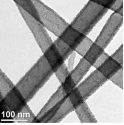
(1) This technique is relatively simple, (2) cost-e ffective (a few thousand dollars) to implement, (3) nano fibers of high surface area to volume ratio from a wide variety of

In this study, therefore, we attended to core and peripheral beliefs, examined the influence of language teachers’ contexts on their work and elicited beliefs through the analysis

A total of 120 interior architecture students were sur- veyed about their experiences on five fields of instruction: (1) course design, learning material and electronic

Hypothesis states that export expansion in manufacturing industry can be explained by export subsidies, real effective exchange rate, labor wages and capacity

How- ever, when both the homo and copolymers of PEI with larger molecular weights (PEIs with 25 kDa molecular weight) either linear (L) or branched (B) were used, the plasmid DNA

The corrosion at the source side under a +3 V DC potential was emphasized by comparing the intensity of the Au4f peaks recorded at a particular position d = 0.5 mm corresponding to