Electrospinning Combined with Atomic Layer Deposition to
Generate Applied Nanomaterials: A Review
Sesha Vempati,
*
Kugalur Shanmugam Ranjith, Fuat Topuz, Necmi Biyikli, and Tamer Uyar
*
Cite This:ACS Appl. Nano Mater. 2020, 3, 6186−6209 Read Online
ACCESS
Metrics & More Article RecommendationsABSTRACT: Combining different material processing techniques is one of the keys to obtain materials that depict synergistic properties. In this review, we have reviewed a combination of two highly potential techniques, namely, electrospinning and atomic layer deposition (ALD), in the view of various applications. Over the past 10 years, our research groups are involved in the exploration of employing this combination for a range of applications. We also include some basic information on both the processes and diversity of nanostructures as a result of their combination. Nonwoven nanofiber membranes are excellent candidates for a wide range of applications. Also, they can act as templates to produce various other kinds of nanostructures when combined with ALD in small/large scale production. These nanostructures could be
used as such or further subjected to other processing techniques yielding hierarchical structures. In this review, we exclusively survey and highlight the unique capabilities of combined electrospinning and ALD for applications in catalysis, photocatalysis, solar cells, batteries and gas sensors.
KEYWORDS: electrospinning, atomic layer deposition, hierarchical nanostructures, catalysis, batteries, sensors, ALD
■
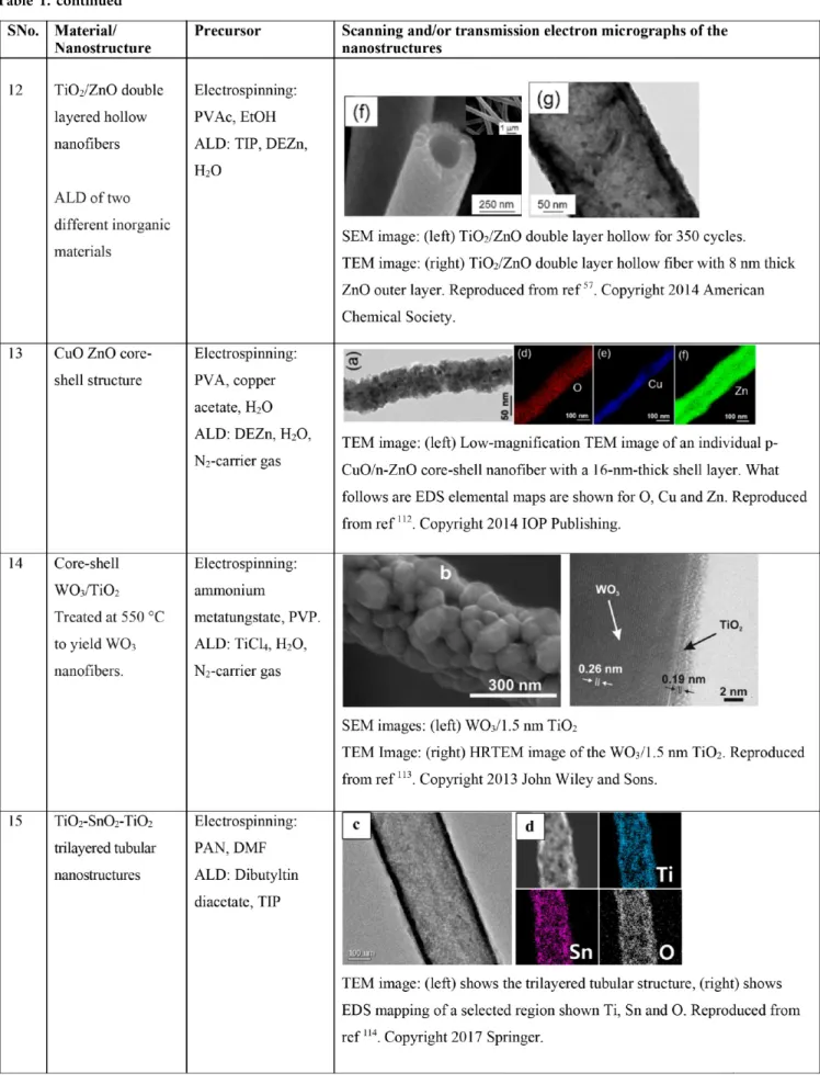
INTRODUCTIONMaterial science crucially includes studies on the properties of various materials and their combinations. Notably, the properties of any material are dependent on the processing methodology. Also, enhancing and tailoring the functionality of an existing material is as important as that of discovering novel counterparts. The intrinsic properties of a material may depend on the physical dimensions, e.g., quantum confinement effect. There is a surge of various material processing techniques asserting some degree of control on the properties and physical dimensions; e.g., pulsed laser deposition,1 chemical vapor deposition,2 hydrothermal growth,3,4 electrospinning,5 atomic layer deposition (ALD),2,6−10 and so on.3,11,12 Now, in the context of enhancing and tailoring the functionality of a material, “combination(s)” of various material processing techniques are promising. The combination of electrospinning and ALD could address the needed high-surface area precision-coated functional materials. Indeed, electrospinning is a versatile technique to produce nanofibers from polymers13 and nonpolymeric14 viscoelasticfluids yielding inorganic and ceramic materials. On the other hand, ALD is capable of producing conformal thinfilms as well as nanostructures (see
Table 1).15,16The materials spectra that can be deposited via ALD includes oxides, nitrides, sulfides, and metals among others.2,6−10Individually, these techniques are rather successful to cover a wide range of applications including energy
storage,17,18 solar cells,19,20 surface passivation,20,21 cataly-sis,22−24 and flexible/wearable devices.25,26 Also, electrospun nanostructuresfind potential usage in (photo)catalysis, energy storage,27solar-cells,28,29filtration,30textile industry,31wound dressing,32drug delivery,33and environmental applications.34
The intersecting research areas of ALD and electrospinning capture significant attention due to the versatile applicability (Chart 1). By looking at the fundamental perspective of high surface area to volume ratio, structural integrity, surface electronic structure, andflexibility are some key requirements for high efficiency, either for catalysis,35 solar cells,36 batteries,37−44 heterogeneous catalysis,4,45,46 antimicrobial activity,47 water purification,48,49 etc. For example, in the case of solar cells, higher current densities could be obtained for a relatively higher surface area of the device.29In the case of catalytic reactions29,45/gas sensors,50 a higher density of the active sites would be exposed to the reactants. It is found that the sensing performance of the core−shell nanostructures results from the radial modulation of the electron depletion
Received: April 26, 2020
Accepted: May 12, 2020
Published: May 12, 2020
Downloaded via BILKENT UNIV on February 5, 2021 at 12:03:04 (UTC).
region as a function of the thickness of the shell.51 Furthermore, due to the band alignment, the hybrid semi-conducting structures, in general, possess an internal electric field. They also depict the tunability of electronic and optical properties.52 This built-in electric field could separate the photogenerated charge carriers before recombination, which has significant potential in solar cells, photodetectors, and photocatalysis.46 These heterostructures facilitate trapping of photons and wavelength selectivity could also be achieved when the photons are suitably confined.53 The combination produces core−shell,54 bishell hollow,55−57 hollow nano-fibers,45,58−62 and metal nanoparticle-loaded47,63−65 nano-fibrous templates (see Chart 1). This combination can be extended to form advanced multilevel structures, such as Al2O3/Ni/Al2O3,
66
SrTiO3/ SrTiO3,
67
polymer/TiO2
/Pt-nanoparticles,68 etc. Furthermore, inorganic material coated
polymerfibers could be subjected to hydrothermal,4chemical bath,69 and microwave-assisted solvothermal70-like methods. For instance, hydrothermal growth4 yields nanorods of high crystalline quality, which provides highly efficient channels for the transport of both electrons and holes to the surface, while the solvothermal technique70 can produce metal−organic frameworks.
As discussed earlier, the application potential of these techniques is reflected in a significant number of publications and patents on catalysis, batteries, and sensor applications (Figure 1). Keeping this in mind, this review covers the literature strictly focusing on the combination of electro-spinning and ALD.Figure 1a shows the year-wise number of publications, whileFigure 1b shows three major corresponding research topics. By given the industrial applicability of these topics, we have also plotted the year-wise number of patents in Table 1. continued
Figure 1c. We start the review by briefly discussing the processes of electrospinning and ALD.
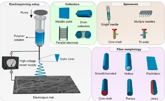
Electrospinning. A charged polymer jet is accelerated (within an electricfield of 105−106V/m) toward the counter
electrode from a fine nozzle forming a Taylor cone.13 The electrostatic repulsion between surface charges induces “splaying” of the cone into several fine strands and continuously drawn nanofibers onto the substrate (counter electrode). The substrate can be, for example a rotating drum, which yields aligned nanofibers when the spinning and collection rates are balanced.71 A cartoon of the electro-spinning process and various types of collecting electrodes are shown in Figure 2. The schematic also shows core−shell, triaxial, and multineedle spinnerets. Such spinnerets, together with the formulation parameters, enable the production of fibers with different morphologies, such as hollow, flat/ribbon, core−shell, porous, and Janus. The electrospinning process has been applied to produce microns to sub-100 nm sized fibers from a rich variety of materials, like polymers, ceramics,
nonpolymeric materials,72 nanocomposites,73 etc. up to the industrial-scale.74−77 Electrospinning also finds vast applic-ability in tissue engineering,78water-treatment,79and the food packing industry.80 It has also been adapted to produce a number of other nanostructures, such as microchannels and tubes,81 porous,82 hollow, or core−shell structures (e.g., biphasic nanofibers with a conducting core with an insulating shell83). It is also possible that the polymers that are intrinsically microporous can be subjected to electrospinning to obtain a relatively higher surface area to volume ratio when compared to that of the nonporous counterparts.82 The polymer of intrinsic microporosity has a high fractional free-volume (26%) and is reported to have a BET surface area of 760 m2/g.84
Up-Scaling of Electrospinning. Apart from optimization of the basic electrospinning parameters, up-scaling of the process usually employs multispinnerets and a suitable power supply. Also certain changes to the collecting electrodes need to be implemented depending on the application. Since the Chart 1. Salient Features of Electrospinning, Atomic Layer Deposition and Their Combination Are Showna
aIt also shows a broad range of hierarchical nanostructures as a result of this combination. The chart also highlights the applicability of these
nanostructures that covers the basic requirements of each of the majorfield of application.
Figure 1.Year-wise statistical analyses on the research topic“electrospinning + atomic layer deposition” (a) number of publications, (b) major research areas, and (c) number of patents. Data updated as of April 24, 2020.
nanofibers are subjected to ALD, it is important to collect the nanofibers such that the additional precursor diffusion step is feasible. In fact, various companies supply the laboratory and industrial-scale components for electrospinning for different applications. They include Spingenix, Inovenso, Bioinicia,
Elmarco, Yflow, IME, RevolutionFibres, Nanofiber Solutions,
Spraybase,Mecc Co., Ltd., and so on. Electrospinning has been successfully exploited in industry. The industrial aspect of electrospun nanofibers is directly visible, where a number of companies around the globe (Europe,85−93 USA,94−96 Asia,97,98Japan,99South Africa,100New Zealand,101) produce nanofibers for various applications. Some of these companies not only design but also manufacture electrospun nanofibrous materials for filter media, biomedical applications, wound dressing, drug delivery systems, textiles, cosmetics and hygiene products, etc. Readers are advised to refer to a review by Persano et al.74and other references74−77for further details on the industrial up-scaling of electrospinning. For large scale production of electrospun nanofibers, multinozzle102 or nozzleless92,100 electrospinning could be employed. The electrospinning yield can be enhanced using alternating current, which relies on an electrostaticfield with periodically changing polarity. Alternating current electrospinning yields multiple times higher productivities achieved with direct current electrospinning.103
Advantages. The major advantages of the electrospinning process can be listed as the following. (1) This technique is relatively simple, (2) cost-effective (a few thousand dollars) to implement, (3) nanofibers of high surface area to volume ratio from a wide variety of polymers and precursors of ceramic, inorganic, and metals, (4) any modification/functionalization is relatively easy, (5) it allows one to produce nanofibers of composites, (6) nanofibers can be collected onto many different surfaces such as glass, metals, water, etc., (7) various nanofibrous structures can be synthesized using hierarchical methods, (8) polymer chain ordering or macromolecular crystallinity increases, and (9) feasibility of industrial level high-volume mass-production.
Disadvantages. There are some disadvantages of the electrospinning process. (1) This technique requires viscoe-lectic precursor, (2) conductivity should be at a moderate level for easy electrospinning, (3) obtaining single crystalline and continuous inorganic fibers are rather difficult, (4) needs the usage of solvents which may be toxic, (5) insufficient cell infiltration and inhomogeneous cell distribution in tissue engineering applications, (6) no/very-limited control on 3D porosity, (7) diameter of the nanofiber cannot be controlled with high precision, and (8) bead formation may be inevitable as the diameter of thefiber decreases, where beads reduce the surface area to volume ratio.
Hardware and Cost of Ownership. Electrospinning is one of the very economical techniques to produce nanofibers. As shown in Figure 2, the setup requires a syringe pump, collection screen, and a high voltage power-supply. Depending on the number of spinning needles (Figure 2), an appropriate power supply needs to be employed so that sufficient current is supplied. Additionally, the whole setup can be installed in an enclosure. This enables continuous spinning where the influence of propellant air is reduced. A lab-scale, commercial setup costs some 1000 USD including a user control on the various features, such as speed of rotating mandrel, duration of the spinning, flow rate in the syringe pump, heating the spinning environment up to 45 °C, and so on. To produce inorganic nanofibers, an oven is required which costs around 1500 USD. Similar to other fiber production techniques, the precursor polymeric materials and relevant solvents are not very expensive. The applicability of this technique to various polymers is one of the most important aspects. When the polymeric nanofibers are used as templates, then a relatively wide distribution of molecular weight of the polymer would still work, reducing the total cost. However, additional cost incurs from the precursor for inorganic nanofibers. Perhaps, during industrial scale production, the evaporated solvent could be recovered through condensing the vapors. This not only makes the whole process cost-effective but also environ-mentally friendly.
Figure 2.Schematic of the electrospinning process. Schematic also shows typical collectors and spinnerets. Reproduced from ref80. Copyright 2020 Elsevier.
Atomic Layer Deposition. ALD is a low-temperature chemical vapor deposition technique where the material growth is governed by sequential self-saturating gas−solid surface reactions.7−10 Conventional gas-phase reactions and thermal decomposition of precursor molecules are eliminated by temporally or spatially separated half-cycles, which leads to digital/pulsedfilm deposition that proceeds with self-limiting ligand-exchange surface reactions only.8,9
The typical unit deposition cycle of a conventional ABAB-type ALD process consists of four steps: (i) dosing of the metal-containing precursor, which reacts with the active surface groups via chemisorption until surface saturation is achieved, (ii) purging step with an inert gas flow, which will completely remove the excess precursor molecules as well as the ligand-exchange reaction byproducts, (iii) dosing of the second precursor, which is in general defined as the coreactant, which likewise reacts with the chemisorbed surface groups via ligand exchange reactions until saturation, (iv) second purging cycle to evacuate the reactor chamber from excess amounts of precursors and reaction byproducts.
As precursor molecules do not react with themselves and both precursors react only with the chemisorbed groups on the substrate surface, gas-phase chemical vapor deposition-type reactions are entirely eliminated. Each unit cycle results in a material deposition of a certainfilm thickness, which is mostly a fraction of a monolayer, and is defined as the growth-per-cycle value.8Under ideal self-limiting conditions, the character-istic growth-per-cycle value would remain constant within a certain temperature range (ALD window) where no thermal decomposition takes place. For certain materials, the conven-tional thermal ALD process at substrate temperatures lower than precursor decomposition does not result in any film deposition. In such cases, plasma-assisted deposition might help in lowering the deposition temperature with the help of energetic coreactant radical species.104The main drawback or risk with plasma-ALD is the possible plasma damage, which might be particularly significant for polymeric electrospun nanofibers. Figure 3 shows a unit plasma-ALD process cycle for AlN, with the precursor (trimethylaluminum-TMA) and plasma coreactant (N2/H2/Ar) exposure events separated by N2/Ar-purge cycles and how these process steps affect the
reactor pressure during the growth experiment.105
Up-Scaling. For the up-scaling of ALD toward industrial-scale high-volume production, deposition rates need to be increased while not sacrificing from the ideal uniformity and conformality. The growth-per-cycle (GPC) parameter in ALD processes is prettyfixed and range typically within 0.5−2.0 Å; however, the total time needed to complete the unit ALD cycle might be further reduced with reactor and precursor pulsing designs. Particularly, “spatial ALD” features dramatically increased the deposition rates where the substrate is physically moved in the spatial domain rather than waiting for purging the active species out of the chamber in the time domain. Using spatial ALD, orders of magnitude higher growth rates have been achieved for several materials. Spatial ALD, therefore, can in principle be applied for the ALD coating of electrospun nanofiber templates as well as where the additional precursor diffusion step needs to be incorporated. Further-more, as the polymeric nanofibrous templates can be woven on flexible substrates, even roll-to-roll ALD processes might be feasible to develop which might further reduce the unit production cost of such ALD-coated nanofiber materials.
Advantages. (1) Thermal ALD yields a very good conformality over large surface areas, (2) scalable up to industrial levels for high-volume production, (3) wide range of inorganic materials toward various application interests can be produced, and (4) novel precursors can be designed and synthesized which might be used for alternative surfaces, materials, and applications.
Disadvantages. (1) Possible chemical reactions between the polymer nanofibers and the ALD-precursor may limit the applicability. As a result, the interface may not be well-defined. (2) Due to the directionality of the plasma-ALD, it requires protective coating on the polymeric template. The plasma-assisted ALD may not yield a uniform coating on the high surface area nanofibrous templates. (3) ALD is limited by the availability of the gaseous precursors with sufficient vapor pressure and high thermal stability.
Hardware and Cost of Ownership. Practically any well-designed ALD reactor, either thermal or plasma-assisted ALD systems are sufficient to provide uniform and conformal coatings on nanofibers or nanoparticle templates. The main requirement is the ALD recipe which will allow the precursor and coreactant molecules to diffuse freely within the nanotemplate. To achieve this condition, conventional thin-film coating ALD recipes are further modified with extra “waiting periods” after the precursor/coreactant molecules are pulsed into the reactor chamber. Typically, for flat substrate coating experiments, the precursor/coreactant pulsing is followed by an immediate N2/Ar purging step, without any
need for an additional waiting period. For nanofiber/ nanoparticle template coating experiments, depending on the effective surface area of the template, additional diffusion periods of 30−180 s are utilized to ensure complete coverage of all available surfaces. On a side note, although we mentioned that plasma-ALD can provide conformal coatings as well, it is also known that plasma processes exhibit inherent direction-ality due to the directionalflow of energetic radicals and ions, which might result in reduced conformal coating performance. In our work,54,55we have demonstrated AlN and GaN coated Figure 3.Temporal process layout for a unit plasma-ALD cycle of AlN and the corresponding variation of the reactor pressure over time. Initially, TMA pulse is introduced into the chamber onto the substrate, which is then adsorbed forming a monolayer. The excess precursor is pumped out. Then reactive N2/H2 plasma species are introduced to the surface which react with the adsorbed TMA to form AlN via ligand-exchange surface reactions. Then unreacted N2/H2 plasma radicals are purged out of the system to prevent subsequent gas-phase reactions. Reproduced from ref 105. Copyright 2019 American Vacuum Society.
nanofibers via plasma-assisted ALD with decent (but not perfect) conformality. Our thermal-ALD coated nanofibers exhibited much improved conformality, as no directional coreactants are present in thermal-ALD experiments. Never-theless, plasma-ALD recipes can be tuned and adjusted to show enhanced conformality, mainly by optimizing the reactor pressure and the related radical residency times within the reactor chamber.
Cost of commercial ALD reactors are typically of less or equal (if heavily equipped with in situ metrology tools) value when compared to widely used PVD systems like sputtering and of significant lower cost when compared to epitaxial growth reactors including MOCVD and MBE. On the other hand, precursor materials are the main consumables for ALD coatings, which are typically expensive if purchased from a few available precursor vendors. This cost item can be reduced if such precursor materials can be synthesized in-house. However, for most of the applications including (photo)-catalysis, energy storage, gas sensing, passivation, and transistor fabrication, typically less-than 20 nm and in some cases just a few monolayer-thick coatings are needed, which makes ALD the only viable option with still relatively low operation cost. In this case, the ownership cost including the consumables further reduces as the expensive precursor can be used for the coating of a high number of samples.
■
ELECTROSPINNING AND ATOMIC LAYER DEPOSITIONThe integration of electrospinning and ALD are schematized in
Figure 4.Figure 4a shows the schematic of a typical unit ALD cycle with precursor dosing and purge steps on a representative nanofiber cross-section. Essentially, precursors are adsorbed at the surface in a sequence and they react to form a conformal coating.Figure 4b depicts steps involved in obtaining various types of one-dimensional fibrous nanostructures, such as nanoparticle-decorated, core−shell, bishell, and so on. It also indicates the optional calcination process to remove the nanofiber core, which converts the nanofibrous structures into hollow nanofibers.
Challenges of Combining Electrospinning and Atomic Layer Deposition. Several critical challenges exist
for an ideal conformal and uniform coating process on electrospun nanofiber template.
(i) Tuning the recipe to provide sufficient precursor diffusion time: In contrast to conventional ALD recipes, to ensure ultimate conformality on the large effective surface area of the nanofiber template, substantially long diffusion time intervals have to be incorporated in the deposition cycle of the material of interest. In order to do this effectively, the gate valve of the reactor chamber is closed right before the precursor pulsing so that maximum amount of precursor vapor is available for diffusing into the porous nanofibrous template. During this diffusion period, the chamber pressure is increased significantly mainly due to the pump isolation and continuous carrier gas flow. The increased chamber pressure might cause additional challenges in the reactor operation, where pressure gauges operate typically at lower pressures. This additional precursor diffusion step is increasing the unit ALD cycle significantly, resulting in extremely long deposition times.
(ii) Keeping the substrate temperature below polymer melting temperature: Despite being known as a low-temperature deposition process, the low-low-temperature compatibility of polymeric materials pose an additional upper limit in substrate temperature to be used in ALD experiments. Typical deposition temperatures lower than 150 °C work for most of the polymers and ALD materials. However, some compounds might require higher temperatures for deposition, which would contradict with the temperature limits of the polymeric material used in electrospun nanofibers. In such a case, an alternative to further reduce the deposition temper-ature would be to employ plasma-ALD at the expense of possible plasma damage and reduced conformality. As an example for this solution approach, we have successfully synthesized AlN coatings on polymer nanofibrous templates by reducing the typical thermal-ALD temper-ature from ∼350 °C to less than 200 °C by using plasma-ALD. Due to the reduced deposition temper-ature, we were able to preserve the volumetricfibrous Figure 4. (a) Schematic representation of a unit ALD cycle and (b) electrospun nanofiber-based synthesis of nanostructures. Inorganic nanoparticle coated core−shell, bishell, hollow, and bishell hollow nanofibers. To prepare these nanostructures, we start with a nanofiber template and a conformal deposition of required material takes place on top of the template. By selectively removing the organic template by calcination, the above listed nanostructures could be obtained. Part a is reproduced from ref106Copyright 2013 John Wiley and Sons.
structure and obtain hollow nanofibers after the calcination process.
(iii) For plasma processes, to avoid plasma etching of the polymeric templates by energetic plasma species, protective layers should be used: Although being useful in reducing the ALD deposition temperature for compound materials, plasma processing comes with several critical shortcomings as well. First, the plasma damage factor might be severe for relatively easy to damage/etch polymeric materials. A possible direct mitigation measure for the plasma damage might be to reduce the rf-plasma power to minimize the incident energy of plasma species and to increase the chamber pressure in order to increase the number of collisions of plasma species, thereby again decreasing the energy of impinging plasma particles. Another indirect mitigation technique that can be used to protect the polymeric materials from degrading under plasma exposure is to use protective layers on the surface of electrospun nanofibers. Such protective conformal layers can be deposited within the same ALD reactor, prior to the plasma deposition process in thermal-ALD mode. Our group has extensively employed this methodology for the fabrication of flexible and hollow-core III-nitride nanofibers. Another significant drawback of plasma-ALD stems from the directional character of plasma processes: this mainly results in a nonideal conformal coating on high surface area nanoporous templates. This effect might be reduced to a certain degree by increasing the pressure inside of the chamber; however, the con-formality performance would definitely not be as good as thermal-ALD processes.
■
PHOTOCATALYSISThe photocatalytic performance of the nanostructures is explored over the degradation of organic pollutants under UV to visible irradiation. The energy of the illumination is mainly determined based on the band gap of the catalyst; however, defects within the band gap could be activated with relatively lower energy. Typically,108 10 mg of the catalyst is immersed in 25 mL solution of methyl orange (10 mg/L). For UV radiation, a 400 W light source with an emission wavelength range of 300−400 nm is employed for the experiments. The light source is kept at a distance of 10 cm, and the solution is kept under UV light for 3 h. A certain amount of sample is collected and centrifuged to eliminate the catalyst (if required), which is then subjected to UV−vis transmission spectroscopy. By tracing the intensity of a characteristic peak of the dye molecule with respect to UV-exposure time, the concentration of the dye molecules is calculated. The photocatalyst is fabricated by depositing catalytically active material (metal oxide semiconductor) on top of the electrospun fibers. Wide band gap metal oxide semiconductors, such as ZnO and TiO2 and their
combina-tions, were employed in different forms like core−shell, nanoparticles, or nanoclusters. They are mostly tested for catalytic activity through the photodegradation of organic molecules (methylene blue, rhodamine B, methyl orange, etc.) in water. The degradation produces CO2or H2O with O2and various molecular fragments.
Comprehensive reviews on semiconductor based photo-catalysts have appeared in the literature.115−117Various studies
on the photocatalytic applications of metal oxide coated electrospunfibers have been studied by our research group by combining electrospinning and ALD.4,35,45,46,68,82,109,118,119In a typical example, core−shell nanofibers were produced where the core is nylon nanofibers while the shell is ZnO nanoparticles or nanolayers.109 As described earlier, a control on the thickness of the shell layer is achieved by varying the number of cycles in the ALD process. Hence, a transition from nanoparticles to a nanolayer with a thickness of ∼27 nm is achieved. The highest photocatalytic activity (PCA) was recorded when the nanoparticles densely cover the surface of the nanofibers, and the activity decreases as the density of the nanoparticle decreases. The enhanced catalytic activity was attributed to their higher catalytic surface area that increases the active sites.109We have further investigated the influence of surface area of a semiconductor layer on the photocatalytic performance,109,119where we varied the mean diameter of the core nanofiber (∼80, ∼240, and ∼650 nm) and keeping the thickness of the shell layerfixed (∼90 nm). The morphological and structural integrity were also investigated, and it is found that ZnO is polycrystalline with a hexagonal wurtzite structure. The nanofibers with the smallest mean diameter showed the highest catalytic performance owing to their higher specific surface area.120Also, the sample could be reused without any significant decay in their PCA. Furthermore, we have improved the catalytic activity by growing ZnO nanoneedles (diameter, ∼25 nm and the aspect ratio of ∼24) using the hydrothermal method on the surface of the nanofibers.4 These hierarchical nanostructures depicted an enhanced catalytic performance which was credited to the surface defects, while the needle structure supports the vectorial transport of photogenerated charge carriers. In connection to the defects, we have studied the intrinsic defect reorganization in ZnO and its effect on the photocatalytic performance with hollow ZnO nanofibers.45 ALD of ZnO with an average grain size of∼20 nm is obtained on nanofibers of two different average diameters (80 and 650 nm). The results revealed that increasing the surface area does not enhance the photocatalytic performance, rather the density of the surface defects play a crucial role. In thefirst glance, it might appear that the defect density is higher if the surface area is increased. However, indeed, there is a critical balance that one has to hit to obtain the highest PCA. Beyond a limit, the increased density of defects decreases the electronic quality, which decreases the quantum efficiency (photon to electron conversion ratio). Clearly, we need to optimize the electronic properties to obtain the highest performance. One of the ways to tune the electronic properties is “doping”. Nasr et al.121 compared the PCA of Al2O3doped ZnO nanotubes with that
of undoped ZnO. By changing the deposition sequences of the Al2O3 and ZnO cycles, Al2O3 doped ZnO nanotubes with
different ratios of Zn/Al were produced. This is rather a potential technique to produce doped semiconductor to increase the carrier concentration. Under UV irradiation, the PCA increased with increasing the ratio of Al2O3/ZnO.
Moreover, the nanotubes could be reused four times without any significant decrease in the catalytic activity. Al2O3doping
of ZnO can indeed decrease the resistivity and increase the carrier concentration.122A higher carrier concentration might have increased the catalytic activity. This method could be applied to other semiconductors. Despite TiO2being another important large band gap material, doped counterparts using ALD are not widely tested for the PCA. By given the stability
and applicability of TiO2, it is certainly a vital testing that still needs to be addressed.
Another important strategy to obtain higher PCA is to delay the recombination process of photogenerated electron−hole pairs through an internal electricfield that arises due to band alignment. Szilagyi et al. reported WO3/TiO2core (140−300 nm)−shell (1.5, 3.1, 10, and 19.3 nm) nanofibers and explored their PCA113 with UV−vis or visible illumination. The nanofibers with 1.5 nm of the TiO2layer showed the highest
visible light catalytic activity. Catalytic activity is brought into the visible region through the WO3core, where the visible light
can penetrate through the thin and wide band gap TiO2shell.
The smart design of structuring wide and smaller band gap materials as shell and core, respectively, is notable. Also, TiO2
is relatively a more stable material under photocatalysis. This protects the core-WO3 material from degradation during the
redox cycles. Santala et al. developed various approaches for the fabrication of catalysts.123Apart from hollow tube and core (NiFe2O4 or CoFe2O4)−shell structures, authors have synthesized hollow tubes filled with Fe2O3 nanoparticles,
where the shell structure is always TiO2.123The highest PCA
was observed for Fe2O3nanoparticle loaded TiO2nanotubes.
Due to the presence of magnetic particles, the catalyst could easily be recovered from the solution and reused. When the catalyst is nonmagnetic in nature, centrifugation is the only quick recovery option if the structural integrity of the catalytic membrane is not good enough. The incorporation of the magnetic nanoparticles not only saves the recovery time but also makes the process easier. PCA of ZnO/ZnAl2O4
multiconcentric nanotubes was studied.108 In this case, the core−shell nanofibers were subjected to two stage calcination. With increasing the number of layers, the formation of defects, Figure 5.Applications of catalyticfibrous materials produced using both electrospinning and ALD. (a) Cartoon illustration of the production of core−shell heterojunction (CSHJ) nanofibers and (b) the PCAs of the ZnO-TiO2 and TiO2−ZnO core−shell heterojunction nanofibers. Constants and exponential decayfits are depicted. (c) Proposed catalysis mechanism: electrons from the TiO2are engaged from the ZnO-TiO2 CSHJ. The energetic band locations of TiO2were taken from the literature. (d) Cartoon illustration of the production of catalytic ruthenium (Ru) nanoparticle decorated PAN carbon nanofibers for MeAB dehydrogenation and (e) plot showing the mole of the formed H2per mole of MeAB versus time during the dehydrogenation of MeAB (cMeAB= 100 mM) catalyzed by Ru@CNF (cRu= 0.0135 mM) at different temperatures, (f) plot depicting the mole of formed H2per mole of MeAB versus time for the 1st to 5th recycle in the Ru@CNF (cRu= 0.0135 mM) catalyzing the dehydrogenation of MeAB (cMeAB= 100 mM) at RT. (g) Schematic illustration for the process for the fabrication of Pt@Nb-TiO2catalyst for ORR and the accelerated-stability test of Pt@Nb-TiO2catalyst having 10 at. % Nb: (h) cyclic voltammetry curves and (i) ORR polarization curves measured at 1600 rpm. First, second, and third rows of thisfigure were reproduced from ref46(Copyright 2014 Royal Society of Chemistry), ref 118(Copyright 2018 American Chemical Society), and ref134(Copyright 2014 American Chemical Society), respectively.
stimulation of nonradiative recombination, and/or surface charge transfer took place in the structures, which significantly enhanced the PCA. So far, it is clear that the electrons and holes take part in the PCA; however, the individual role of each of the excited state carriers in the catalysis is not known. In this direction, our group has employed a core−shell heterojunction nanostructure based on TiO2and ZnO that can
selectively expose either of the charge carriers to the environment (Figure 5a−c).46 Given the band alignment between the core and shell materials, electrons or holes are selectively exposed to the catalytic environment under appropriate illumination (Figure 5c). Essentially, when the shell is TiO2, electrons remain in the conduction band of TiO2 while the holes may migrate to the valence band of ZnO. The electrons in the conduction band when available at the surface take part in the catalysis process. The converse is true if the shell layer is ZnO and the core is TiO2. Indeed, these kinds of
catalysts must be tested for other synthesis applications where one requires predominantly electrons or holes in the reactions Apart from the excited state carriers, the defects at the surface also play a crucial role in determining the rate of PCA. At the TiO2 (ZnO) surface, electrons (holes) from the conduction (valence) band may be captured by oxygen vacancies. We found that the catalytic activity is 1.6 times higher when holes are involved in the catalytic activity, i.e., TiO2−ZnO core− shell heterojunction where lower mobility of holes and oxygen vacancies play a crucial role.46In the case of the TiO2−ZnO core−shell heterojunction, the defect bound electrons and holes take part in the catalytic reaction, where the efficiency is limited by the recombination time-scale and their availability at the surface. The energy from the defect electrons could be captured, as shown by Aslan et al. with Pd/ZnO/polyacryloni-trile nanofibers.35In their study,35anisotropic Pd nanocubes were attached by submerging the nanofibers in the dispersion of Pd nanocubes for 30 min and drying at 110°C for 5 min. Pd/ZnO nanofibers depicted better performance than that of ZnO nanofibers, which was attributed to both energy transfer between the Pd nanocubes and the ZnO nanolayer and plasmonic resonance excited by the defect electrons of the ZnO layer.35 The basic idea of capturing the photoexcited electrons and deploying them for PCA can be extended to other material combinations including noble metals such as Au. Also, these noble metals can increase the applicability by taking part in metal catalyzed chemical reactions. Bechelany et al. reported the preparation of metal organic framework (MOFs) and projected their possible use in photocatalysis, where ultrathin oxide (40−50 nm thick ZnO and Al2O3) layers
on PAN nanofibers were subjected to microwave-assisted solvothermal treatment.70 The characterization of the final product revealed a specific surface area of SBET= 1760± 260 m2 per gram while ZnO deposited PAN nanofibers have a
specific surface area (SBET) of 10 m2/g. As discussed earlier,
increasing the surface area of the catalyst is a vital task, where a balance needs to be achieved with respect to the surface defects so that the overall optical quality of the catalyst is not compromised. MOFs have grabbed serious research attention which, however, is not thoroughly exploited for PCA with hierarchical structure.
Reduction, Dehydrogenation, and Hydrolysis Reac-tions. Chemical transformation of small organic molecules is a rather important field of research, where nanostructures are widely applicable as catalysts. This is due to their higher specific surface area to volume ratio requiring a relatively
smaller quantity of the catalyst with respect to their bulk counterparts. Celebioglu et al. studied the reduction of 4-nitrophenol with core (polyacrylonitrile)−shell (TiO2, 8 nm)
decorated with Pt nanoparticles (2 nm mean diameter).124It is found that the deposition of a thin layer of TiO2enhances the
stability of the polymer and improves the attachment of Pt nanoparticles. Also, the nanofibers could be reused several times without any significant change in the fiber morphology at a degradation rate of 0.1102 s−1. In a recent study, Pd nanoparticles (∼4 nm in diameter) are coated on top of cross-linked cyclodextrin nanofibers and employed for the hydro-genation of 4-nitrophenol.125 Khalily et al. studied hydrolytic dehydrogenation of methylamine borane (MeAB) with Ru/ carbon nanofibers.118 The electrospun PAN nanofibers were carbonized and functionalized with Ru quantum dots of 3.4± 0.4 nm (Figure 5d). The volume of hydrogen quantifies the catalytic activity which measured during the hydrolytic dehydrogenation of MeAB (Figure 5e). In a control measure-ment, Ru-free carbonized nanofibers depicted no catalytic activity. The rate constants (kobs) for the reactions were, respectively, 0.00163, 0.0458, 0.0763, and 0.2033 mol H2/(mol
MeAB × min) at 15, 20, 25, and 30 °C. Furthermore, the activation energy (Ea) for the dehydrogenation of MeAB by
Ru@CNF was found to be 30.1 kJ/mol, which was much lower than most catalytic systems reported in the literature. Moreover, the catalytic stability of the Ru@CNF was evaluated overfive repetitive cycles, and the nanofibers could completely convert the MeAB by retaining 72% of its intrinsic catalytic performance even at the fifth recycle (Figure 5f). In another study,126TiO2hollow nanofibers were used to grow MOFs on
thefibers through solvothermal synthesis. The resultant fibers were tested for the hydrolysis of methyl paraoxon where the formation of 4-nitrophoxide was observed by monitoring the UV−vis absorption band at 407 nm.126 PVDF/Ti(OH)4 and PMMA/Ti(OH)4 nanofibers were subjected to 200 ALD
cycles to form TiO2. Then solvothermal synthesis was employed for the synthesis of UiO-66-NH2 crystals. During
the solvothermal process, the PMMA core was removed, leading to hollow fibers, while the PVDF core remained. Hollowfibers with MOF crystals have a specific surface area of 264 m2 g−1. Osman et al. produced catalytic PAN nanofiber
functionalized nanoparticles of ZnO and Pd nanocubes for 2,4,6-trinitrotoluene (TNT) reduction (nitro groups of TNT into amine groups).127 Pd nanocubes were coated on top of PAN/ZnO nanofibers. Indeed, the catalysis using the nanostructures is limited to the conversion of small molecules. However, there is an unexplored and huge potential that exists with these nanostructured catalysts. The advantage is not just limited to the high surface area to volume ratio, it extends to higher density of surface bound active sites with multilevel hierarchical structures. Furthermore, the nanostructured catalysts can be recovered easily from the reactants. If suitably explored, we speculate that these catalystsfind applications in biphasic interfacial reactions, where the catalytic membrane at the interface separates reactants and products into two different phases. Since the surface functional groups determine the hydrophilic and hydrophobic nature of the polymer, this could be a very good starting point.
Electrochemical Catalysis, H2O Splitting. Similar to
photocatalysis, the activity of (photo)electrochemical catalysis crucially depends on the electronic properties of the catalyst in conjunction with carrier-concentration and its chemical potential with reference to the redox potential of water. It is
important that the stability of the catalyst depends on the choice of the material where the chemical potential is an intrinsic property. Our research group recently tested NiOOH/Ni(OH)2decoratedflexible carbonized PIM fibers.
82 Thefibers showed a low onset potential (ηHER=−40 and ηOER
= 290 mV vs RHE), small overpotential atη at 10 mA cm−2 (hydrogen evolution reaction (HER) =−147 mV and oxygen
evolution reaction (OER) = 390.5 mV), outstanding kinetics (Tafel slopes for HER = 41 mV dec−1 and OER = 50 mV dec−1), and high stability (>16 h) for water splitting in 0.1 M KOH. MWCNT/TiO2nanofibers were also tested,
128 where the current densities were found to be 5.1, 4.4, 2.6, 1.7, and 1.0 mA/cm2 for 20, 10, 5, 2, and 0% of MWCNT in TiO2,
respectively. Doping of a semiconductor increases the carrier Figure 6.(a) J−V characteristics of TiO2nanofiber devices with four different TiO2nanofiber layer thicknesses, from 2 μm (open square), to 3.8 μm (solid circle), to 4.5 μm (open diamond), and to 5.4 μm (solid triangle). (b) Incident photocurrent conversion effciency (IPCE) curves for the bare SrTiO3(STO) and STO@ZnO300Cphotoanodes, where ZnO300Cindicates 300 cycles of ALD of ZnO on STOfibers. The presence of ZnO promotes the photon absorption and collection via the bandgap transition of STO. In addition, the IPCE reached a maximum of∼16.43% at ∼380 nm for the STO@ZnO hybrid photoanode, which is∼44 times to that of bare STO at ∼370 nm (i.e., ∼0.37%). (c) Schematic diagram depicting the synthesis of the SnO2/TiO2double-shell nanostructure and lithium-ion insertion and extraction. Polyacrylonitrile nanofibers were subjected to ALD of SnO2and then TiO2. The TiO2outer shell maintains the structural integrity of the electrode during the charge−discharge cycles, where significant internal stress is expected due to the volume expansion. In fact, the hollow nature accommodates the volume expansion. (d) Synthesis and design of the 3D FSiGCNFs. (top row) Illustration of the synthesis process of the 3D FSiGCNFs. The 3D FSiGCNFs were soaked in hydrochloric acid solution to remove the NiO to form precise and controllable expansion space and annealed at 800°C in Ar atmosphere for 2 h. (middle row) Schematic diagram of the 3D FSiGCNF electrode design. Rationally designed FSiGCNFs with precise control of the expansion space by ALD, followed by electrospinning, were used as protection of Si NPs forflexible and binder-free lithium-ion batteries. The graphene/carbon matrix with excellent mechanical strength and electron transport properties not only achieves a superfast electron transfer but also provides enough space to buffer the volume changes of Si NPs during the lithium insertion and extraction reactions. In addition, the stable SEI forms outside of the graphene/carbon matrix rather than on the surface of Si NPs, which is attributed to the electrolyte being blocked by the hierarchical porous graphene/carbon matrix, while facilitating lithium transport throughout the whole structure. The 3D FSiGCNFs can keep the overall morphology, and the SEI outside the graphene/carbon matrix is not ruptured and remains thin after deep electrochemical cycles. Illustration of (bottom row) electron transmission and Li+storage in the 3D FSiGCNFfilm. Parts a, b, c, and d are reproduced from ref36(Copyright 2013 Elsevier), ref67 (Copyright 2018 Royal Society of Chemistry), ref 56(Copyright 2013 Royal Society of Chemistry), and ref 44 (Copyright 2016 American Chemical Society), respectively.
concentration and may introduce in-gap states that could be used for visible light harvesting. ALD is a very promising technique for doping the wide band gap semiconductors, and a large scope is visible for future development of the catalysts for water splitting. Nitrogen doping of TiO2 is one such example.129 After doping, the hydrogen evolution capability and a 10-fold improvement (0.09 to 0.8%) were observed in the photoconversion efficiency. Du et al. reported niobium-doped titania-supported Pt catalysts (Pt@Nb-TiO2).130 First, niobium-doped titania (Nb-TiO2) nanofibrous membrane was
produced using poly(vinyl acetate), titanium(IV) isopropoxide, and niobium ethoxide (Figure 5g). The nanofibers were pyrolyzed in air at 500°C for 24 h to yield Nb-TiO2 fibers. After the deposition of Pt nanoparticles of various sizes (depending on the applied ALD cycle), Pt@Nb-TiO2 fibers were tested for the oxygen reduction reaction (ORR). The area-specific ORR activities of the catalysts rose from 0.0084 to 0.28 mA/cm2for Pt@TiO2 while it reached 0.9 V (vs RHE)
when doped with 10 at. % Nb (Figure 5h,i. The accelerated-stability test on the Pt@Nb-TiO2revealed a very high stability
with ∼10% loss in activity. Recently, Khalily et al. reported Co3O4 nanocrystals (∼3 nm mean diameter) decorated with
nitrogen doped carbon nanofibers for ORR and oxygen evolution reactions (OER).131 An onset potential of 0.87 V with a Tafel slope of 119 mV dec−1 was observed, which is close to the performance of a commercial Pt/C catalyst. The turnover frequency value was calculated at an overpotential of 550 mV to be∼0.14 s−1, which is∼15 and 3-fold higher than those of the standard IrOx (0.0089 s−1) and bulk Co (0.05 s−1) catalysts. Further on, with the carbon nanofiber electrodes, recently, self-supported electrodes with Ni/NiO and Pd nanoparticles are employed for HER/OER.132 The best CNF-Ni/NiO-Pd electrode displayed the lowest overpotential (63 mV and 1.6 V at j = 10 mA/cm2), a small Tafel slope (72 and 272 mV/dec), and an exchange current density (1.15 and 22.4 mA/cm2) during HER and OER, respectively. Notably, these electrodes consist of graphitic layers that cover and protect the Ni/NiO NPs from corrosion. Photo/electro-chemical activity of the TiO2 surface is already well know. Indeed, TiO2coated poly(acrylonitrile)fibers were employed
for HER through biological species, viz, Escherichia coli.133The TiO2 coated membranes were then functionalized with a
[NiFe]-hydrogenase-containing membrane fraction from Es-cherichia coli. This hierarchical structure generates an organic film around the fiber mat which depicts the electrochemical activity for HER, where the current densities were more than 500 mA/cm2at 0.3 V overpotential.
■
ENERGY: GENERATION AND STORAGEOne of the methods to convert renewable energy to electric power is deploy solar cells. Li et al.36 compared the photovoltaic device performances of the FTO/TiO2-HBL/ TiO2-nanofibers-dye/P3HT/PEDOT:PSS/Au device
struc-ture, where TiO2-HBL (hole blocking layer) is prepared via ALD or spin-coating. Pinhole free structurally integral ALD-TiO2 film depicted a relatively higher efficiency, due to reduced dark leakage current and increased charge carrier lifetime. See Figure 6a for JV curves from this DSSC. A number of studies employed electrospun nanofiber as active junction material, especially in dye sensitized solar cells (DSSCs). The applicability of electrospun nanofibers is due to the high surface area to volume ratio. However, the morphology that results from electrospun nanofibers consists
of a large density of grain boundaries where the generated charge carrier could be trapped. This trapping could be detrimental for the efficiency of the device. Notably, the conformal coating that could be obtained from ALD is least explored when combined with the electrospun nanofibers. Much of the research focus is needed on how to reduce the grain boundaries through the ALD.
Apart from solar cells, photoelectrochemical splitting is another methodology to produce energy. As discussed earlier in the sectionPhotocatalysis, impeding the e/h recombination is essential for higher catalytic activity. Similarly, it is the case with photoelectrohcemical activity. For instance, the internal electric field between SrTiO3 (STO) nanofibers and ALD coated ZnO film hindered the e/h recombination and enhanced the photoelectrochemical activity. This heterojunc-tion, depicted a promising photocurrent stability of∼61.3 μA/ cm2, which was ∼600 times higher than that of the pristine STO homojunction counterpart (0.12μA/cm2).67
SeeFigure 6b for incident photon-to-current conversion efficiency with reference to the wavelength.
Energy that has been produced from the renewable natural sources (solar energy, wind energy) needs to be stored in the form of electrochemical energy with the help of batteries and supercapacitors. Earlier investigations37−44aim at the develop-ment of new and next generation electrochemical energy storage technologies due to the ever increasing demand for energy. Over the current trend, lithium-ion batteries are promising power storage devices in the smart and portable electronic devices due to relatively higher specific power density which is rather an important factor for commercializa-tion. This is where the high surface area to volume ratio of nanofibers plays a crucial role which can support higher current densities with three-dimensional architecture.
Generally, the development is focused on the construction of a new set of electrode materials or assemblies to produce efficient, stable, and cost-effective energy storage applications, where highly efficient electrochemical activity, shorter ionic path, and high electrical conduction are efficiency determining factors.44 Commonly, graphite based electrode systems are used as an anode material in lithium-ion batteries due to higher stability, good electrical conductivity, and relatively lower cost. Alternative anode-materials such as MoS2,
37
Sn,38 Ge,39 and carbon38,40,41have also been studied for lithium and sodium ion batteries.37−43 To improve the storage-efficiency, it is crucial to design a hierarchical nanoarchitecture, where the combination of electrospinning and ALD play a crucial role. Among the low-dimensional electrode materials, continuous 1D electrospun nanofibers have grabbed the attention as promising electrode materials with intriguing properties when compared with the electrode systems synthesized through other approaches. Also, electrospun nanofibers have an additional advantage such as scalability.27 Readers are encouraged to go through a comprehensive review that covers the secondary batteries based on electron spun nanofibers.27 The most important role of ALD, in this case, is to produce highly conformal coatings (TiO2,38,39Al2O341,42) that not only
protect the active material from pulverization, cracking, etc. but also changes the surface functionality to the hydrophilic nature enhancing the electrolyte uptake. Furthermore, the TiO2layer
inhibits the reactions with lithium or sodium and enhances the stability of the electrodes. On the other hand, Ru40and Sn,38 like heavy metals, are deposited in the form of nanoparticles on the surface of the protective coating40or directly on top of the
electrode,38 which in both cases the conductivity of the electrode increases. Normally nanoparticles are aggregated which results in the unstable specific surface area. This instability lowers the overall performance of secondary batteries, where relatively high capacitance and long-term stability are compromised.
Jean et al.114studied an electrode material based on TiO2
-SnO2-TiO2 trilayered tubular nanostructures. The electrode depicted high reversible stability of∼550 mA h/g even after 60 cycles at a current density of ∼50 mA/g. The sandwich architecture accommodated the mechanical stress during the charge−discharge cycles and improved the electrochemical properties. On the other hand, SnO2-TiO2 double shell nanotubes depicted stable and reversible capacity with higher current density than that of single SnO2and TiO2 nanotube electrode assemblies.56Figure 6c shows a schematic of lithium ion insertion and extraction. Electrospun Si-loaded carbon nanofibers with alumina coating were tested for electro-chemical performance, and it is found that alumina coating increases the mechanical integrity, stability, and prevents any unwanted reactions between electrode and electrolyte.135This is where the conformality of ALD is apparent. Furthermore, as expected, the thickness of the alumina determines the resistance to the transfer of charge. Also alumina coating improves the capacitance retention from 36.1% to 82.3% for 28 cycles of ALD when compared to that of uncoated Si/C nanofibers. Zhu et al.44developed aflexible anode for lithium ion batteries. In their report, a 3D architecture of flexible silicon and graphene/carbon nanofibers (FSiGCNFs) is studied where an atomic-scale control of the expansion space is obtained without any binder.Figure 6d shows the detailed schematic of the fabrication and ion exchange process. During the charge−discharge cycles, Si nanoparticles depict volume expansion, where in FSiGCNFs the Si nanoparticles are surrounded by accurate and controllable void spaces. This readily increases the structural stability where the void spaces minimize any damage due to the volume expansion. This 3D porous structure with built-in void space between the Si and graphene/carbon matrix not only limits most solid electrolyte interface formation at the outer surface, instead of on the surface of individual NPs, and increases its stability. As a result, highly efficient channels were produced for the fast transport of both electrons and lithium ions during cycling. The electro-chemical performance of FSiGCNFs is significant indeed, viz, 2002 mAh g−1at a current density of 700 mA g−1over 1050 cycles corresponding to 3840 mAh g−1for silicon alone and 582 mAh g−1at the highest current density of 28 000 mA g−1. A conformal coating of Sn on carbon nanofibers increased the conductivity, while TiO2 coating is employed as a
protective coating.38The pipe-wire form of TiO2-Sn@carbon resulted in relatively higher capacity. Also, more stable cycle performances are recorded with both lithium (643 mAh/g at 200 mA/g after 1100 cycles) and sodium ion (413 mAh/g at 100 mA/g after 400 cycles) batteries. TiO2coated germanium
and graphene composites are tested for efficiency as anode materials.39The specific capacity of TiO2coated composite is
1050 mA h/g (100th cycle) and 182 mA h/g (250th cycle) for the lithium and sodium ion batteries, respectively. These values have shown significant improvement from pristine germanium and germanium/graphene nanofibers. Ru-nanoparticles/TiO2
on nitrogen doped carbon nanofibers depicted higher mass transport and electrical conductivity while Ru-nanoparticles increased the round-trip efficiency.40 Theoretical results
indicated that Ru and TiO2 enhance the electron transport capacity of Li2O2 when compared to that of pristine carbon
nanofiber network. Among TiO2/MoS2 and pristine MoS2 nanofibers,37 the latter depicted an efficient discharge capacitance of 840 mA h/g2 at the second cycle and the
excellent rate capacity than that of bulk MoS2. Also, ∼30%
retention capacity is observed. Here, ∼4 nm of TiO2 film protects the sulfur dissolution during the cyclic process; however, the authors observed some reduced storage capacitance and increased retention (up to ∼64%) after 30 cycles. Apart from the expensive lithium based battery technologies, sulfur-based systems have been tested owing to the advantages of lower cost, acceptable energy density, and sustainability.41,43Fe2O3-carbon nanofibers were subjected to
vapor phase sulfidation at 600 °C under vacuum to produce FeS2-carbon nanofibers for Li-S batteries (electrolytes:
conven-tional carbonate electrolyte and a“solvent-in-salt”-type).41Due to vacuum and thermal processing, the electrode surface is now binder-free and depicted a cycling stability (working voltages with reference to Li/Li+) of 1.5−3.0 V with carbonate electrolyte and in solvent. When the surface is coated with 50 nm of Al2O3 on the FeS2-carbon nanofiber, the cycling
stability of the Li-FeS2system is increased to 1.0−3.0 V along with the high discharge energy density at both the material level (∼1300 Wh/kg) and electrode level (∼1000 Wh/kg). In another example, porous C/BaTiO3 nonwoven nanofibers
were initially stabilized at 280 °C for 4 h in air and then carbonized at 900°C for another 6 h at 2 K/min heating rate under N2atmosphere. Then the porous C/BaTiO3mats were treated with sulfur powder (heated to 160°C for 10 h under vacuum and then raised to 260 °C for 1 h in an Ar-filled tubular furnace) followed by ALD coating of TiO2. The
heterostructure depicted discharge capacitances of 524.8 and 382 mA h/g after 1400 at 1 A/g and 3000 cycles at 2 A/g, respectively. This results from the inhibition of the volume expansion and shuttle effect, effective utilization of the active material, and formation of an interface with stable ionic transport channels. Yan et al.3 compared various methods of synthesis of V2O5 and found that the electrospun V2O5 nanofibers depicted relatively higher specific capacitance of 190 F/g in aqueous electrolyte (2 M KCl) and 250 F/g in organic electrolyte (1 M LiClO4) with energy densities of 5
Wh/kg and 78 Wh/kg, respectively.136 The specific capaci-tance is comparatively lower (150 F/g in aqueous electrolyte) when V2O5is loaded on top of a carbonfiber as a composite. Also, the energy density turned out to be lower, viz, 18.8 Wh/ kg.137With the lack of commercial devices, indeed application-oriented process research requires more attention so that the viable techniques such as electrospinning and ALD will lead to a commercial device, however, with not undermining the fundamental research. Notably, commercialization of such energy storage devices requires multistage research on various aspects. It is ideal to implement industrial research projects so that the researchers while perusing a scientific idea would be able to extend the thought process until the stage of commercialization.
■
GAS SENSORSThe nanostructured form of hierarchical 1D assemblies of wide band gap semiconductors such as ZnO,50,51,57,60,61,138−140 SnO2,65,111,140TiO2,50,51,57including CuO (ref112) depicted
unique surface functionalities and higher sensitivities toward ethanol,138 O2,51,60,140 NO2,57,60,65,139,140 CO,57,60,65,112,139
NH3,
50,65 H2,
65,111
etc. The basic principle of gas sensing is as follows. In the case of semiconductors, when the gas molecule adsorbs at the surface, the free electrons (hole) in the conduction band (valence band) may be captured by the gas molecule and/or adsorbed at the defect. The shift of charge can be partial or complete depending on the adsorbing species and availability of the unoccupied states. Since the carrier density is decreased upon adsorption, a change in the conductivity could be expected. As the concentration of the test gas molecule increases, the trapped charge density also
increases, thus the conductivity decreases. A calibration curve is obtained by recording the change in the electrical conductivity with reference to the concentration of the test gas, from which the sensitivity can also be calculated. A schematic of a typical gas sensor is shown inFigure 7a. Despite the whole process appearing to be simple, the dynamics of adsorption and desorption and the mechanism of sensing determine not only the selectivity and sensitivity but also the time-based response. Since the adsorption and desorption Figure 7.(a) Schematic process of fabrication of a sensor device with ZnO hollowfibers on SiO2/Si. The interdigital electrode pattern Ti/Pt is deposited on top of ZnO hollowfibers. The electrical characteristics are recorded with reference to the concentration of the test gas. (b) Dynamic response of the ZnO nanofiber based sensor to O2. The inset is the enlarged part of the data obtained at 300 ppm of O2. (c) Variation of sensitivity as a function of O2concentration. Electro optical response of theΩ-shaped SnO2@ZnO based photodetector is shown from parts f to h. (f) IV curves from the SnO2and SnO2-ZnO under illumination of 280 nm wavelength light compared with that of the dark. The IV curves almost overlap across the two types of devices, while the photocurrent depicted a significant difference. The hybrid structure reaches 0.1 μA at 5 V. (g) Spectral responsivity is compared across SnO2and SnO2@ZnO photodetectors. The hybrid detector is∼30 times more responsive than the pure SnO2 counterpart with a shift of cut off wavelength to 290 nm from 308 nm. The observed improvements are attributed to their type-II band alignment and built-in electricfield as shown in part h. Under UV illumination, electrons tend to move into SnO2while holes to the ZnO shell. Part a, parts b−e, and parts f−h are reproduced from ref 60(Copyright 2014 Institute of Physics), ref140 (Copyright 2009 Institute of Physics), and ref 53(Copyright 2017 John Wiley and Sons), respectively.
processes are required to take place sequentially, the sensors are operated at relatively higher temperatures.
Ethanol sensitivity is tested on the tubular assembly of ZnO nanostructures while varying the thickness of the shell and the operating temperature.138The lower the thickness of the wall, the better the responsivity when tested within a thickness-range of 10−50 nm. Authors report that for a sample of a 10 nm thick shell, the surface is completely depleted and thus they observed the highest response to the rest of the vapor at a sensing temperature of 450°C. Further into the sensing, O2,
NO2, and CO gases have been tested on ZnO nanotubes,
where the sensitivity of the sensor to CO gas depends on the thickness of the shell,60 however, better than that of ZnO nanofibers.61 The calcination temperature (determines its crystallinity) at which the process of transforming the core− shell nanofiber into the tube (sacrificial polymer core) also plays a crucial role. The formation of nanograin assemblies in the fiber-network is the key for higher sensitivity. Other studies139have focused on the diameter of the nanotube (fixed wall thickness of∼60 nm) on the sensitivity toward CO and NO2 exposure. At a critical thickness of the wall, high
selectivity is observed with CO gas over H2, benzene, and toluene gases. SnO2nanotubes were studied for sensitivity of
ethanol over H2, CO, NH3, and NO2 gases,
65
where the thickness of the shell wall has been varied from 8 to 37 nm. Twisting the sacrificial PAN nanofibers and depositing the SnO2layer resulted in SnO2nanotube microyarns.111A stable and reversible H2 response is obtained for a diameter of 500
nm and a wall thickness of 70 nm. The width of the depleted and undepleted regions determine the change in the resistance of the device and hence the sensitivity.
ALD of two different inorganic materials (TiO2 and ZnO)
on a sacrificial electrospun nanofiber yields double layered hollow nanofibers (seeTable 1). These heterostructures were tested for gas sensitivity with CO and NO2 as a function of
thickness of the shell.57The results suggested that the double layer hollow fibers were more efficient than that of hollow fibers in terms of sensitivity toward reducing gases, however, quite lower responses for oxidizing gases. Core−shell structured TiO2-ZnO nanofibers depicted better sensing
response toward NH3 than that of ZnO-TiO2 due to higher sensitivity of the ZnO-shell.50On the other hand, SnO2-ZnO
based core−shell nanofibers were tested for O2 and NO2 sensitivities which performed better than pristine ZnO nanofibers.140
The time-dependent response of SnO2-ZnO in
the presence of O2 is shown in Figure 7b−e for various gas
concentrations. Core−shell TiO2-ZnO nanofibers were tested
for O2 sensing.51When O2is adsorbed at the surface on the ZnO layer, the depth of the surface depletion layer changes and that is reflected in the resistivity. An ultrathin shell (∼10 nm) of ZnO on the SnO2 nanofibers resulted in a notable
sensing response and selectivity over their pristine counter-parts, where the selectivity was associated with the depletion layer at the surface.141 The improvement in the sensing performance may be attributed to the formation of a heterointerface, surface depletion layer and the internal electric field created at the interface. Core−shell structured CuO (p-type) and ZnO (n-(p-type) was tested for CO gas sensing.112As in the case of tubular nanostructures,50,60,139 the thickness of the surface ZnO layer and the width of the depletion layer is vital to determine the responsivity. This core−shell structure depicted a low sensing detection limit than that of pristine ZnO and CuO nanofibers. By an appropriate choice of the
thickness of the active layer/the top ZnO layer,60,139 a relatively higher sensitivity to the reducing gas may be obtained. The thickness of the shell modulates the depth of the depletion layer radially142 and can also influence the response time.50Nevertheless, the response of the ZnO based sensor to O2is inherently a slow process, where the oxygen can
be adsorbed at the surface as well as at the defect sites, capturing an electron from the conduction band or defect site, respectively. Release of defect-bound-oxygen requires a free hole in the valence band which could be mediated by a photon of suitable energy. Indeed a sensor based on the spectral response will be discussed. By producing ZnO of higher optical quality or lesser oxygen vacancies through ALD, we may expect a faster response from the sensor. Despite a potential material spectrum that ALD is capable of, only a limited number of materials are tested for sensitivity by producing hierarchical structures. There is a lot of scope in the context of Schottky junctions where one can expect faster response and better selectivity. The functionality of the earlier discussed gas-sensors depends on the change in the electrical resistivity due to the presence of the test gas molecule. Instead of electrical means, interestingly, Viter et al.143 investigated gas-detection by monitoring the photoluminescence (PL) of ZnO-PAN nanofibers. By monitoring the ratio of intensities from near band edge emission (NBE) and deep level defect emissions (DLE), the concentrations of the volatile organic compounds are detected. Ethanol vapor (150 ppm) caused∼20% and 30% for NBE and DLE intensity variations, respectively. This sensitivity is indeed relatively low when compared to the sensors based on variation in the conductivity. The sensitivity of this particular sensor depends on the simultaneous intensity of the two peaks in the PL spectrum, and this device may be suitable for recognition of different volatile organic com-pounds. Viter et al.143 also showed that the PL signal is stronger from ZnO-PAN nanofibers than that of ZnO on Si substrate for the same quantity of the ZnO due to a large improvement in the specific surface area of the nanofibers. A spectrographic approach to gas sensors is know, and most of the studies use electrical signal to sense a test gas. The easiness in operation of gas sensors based on an electrical signal is completely acknowledged. However, when the device response is either low or slow, one might explore the possibility of a spectroscopic approach for improved results. Notably, the nanostructures act as waveguides increasing the detection efficiency.
■
PHOTODETECTORSUV response from wideband semiconductors, such as ZnO, TiO2, SnO2, etc., has been extensively studied in their pristine
form as well as in heterointerfaces.53,64,110,144 For instance, nanotubes of ZnO [ref144] and TiO2[ref64] were employed
as active materials in detectors, while the heterointerfaces include BiVO4-ZnO110 and SnO2-ZnO.53 Upon
UV-illumina-tion, the absorbed photons create electron−hole pairs. A certain fraction of these electron−hole pairs may form excitons followed by recombination which does not change the free carrier concentration. However, on the other hand, the free carriers, including dissociated excitons, transiently increase the carrier concentration. The change in the free carrier concentration increases the conductivity resulting in an electrical signal. This is the basic detection mechanism of a photon in a photodetector. Chaaya et al.144 reported the sensitive and stable UV sensing properties of ZnO nanotubes