Electronic structure of the contact between carbon nanotube and metal electrodes
S. Dag, O. Gülseren, S. Ciraci, and T. Yildirim
Citation: Appl. Phys. Lett. 83, 3180 (2003); doi: 10.1063/1.1616662 View online: http://dx.doi.org/10.1063/1.1616662
View Table of Contents: http://aip.scitation.org/toc/apl/83/15
Published by the American Institute of Physics
Articles you may be interested in
Effects of local structural defects on the electron transport in a carbon nanotube between Cu electrodes
Applied Physics Letters 97, 242112 (2010); 10.1063/1.3527918
First-principles study of contact between Ti surface and semiconducting carbon nanotube
Electronic structure of the contact between carbon nanotube and metal
electrodes
S. Dag, O. Gu¨lseren, and S. Ciracia)
Department of Physics, Bilkent University, Ankara 06800, Turkey T. Yildirim
NIST Center for Neutron Research, National Institute of Standards and Technology, Gaithersburg, Maryland 20899
共Received 4 June 2003; accepted 12 August 2003兲
Our first-principles study of the contact between a semiconducting single-walled carbon nanotube 共s-SWNT兲 and metal electrodes shows that the electronic structure and potential depend strongly on the type of metal. The s-SWNT is weakly side-bonded to the gold surface with minute charge rearrangement and remains semiconducting. A finite potential barrier forms at the contact region. In contrast, the molybdenum surface forms strong bonds, resulting in significant charge transfer and metallicity at the contact. The radial deformation of the tube lowers the potential barrier at the contact and increases the state density at the Fermi level. © 2003 American Institute of Physics. 关DOI: 10.1063/1.1616662兴
Nanoscience and nanotechnology have opened a new frontier aiming at the ultimate miniaturization of electronic circuits with ultrahigh speed and high-density components presenting new functionalities. The switching of the current in a semiconducting single-walled carbon nanotube 共s-SWNT兲 at room temperature by an external electric field has been utilized to fabricate new field-effect transistors 共FET兲.1–3The interaction between s-SWNT and metal
elec-trode, and the Schottky barrier,⌽B formed thereof have been
proposed as the origin of FET operation. Model calculations have been carried out to provide further understanding of experimental I – V characteristics.4,5 The SWNT–electrode interaction and resulting electronic structure are crucial for the electron transport and hence for all device properties. This letter presents an analysis of the self-consistent-field 共SCF兲 electronic potential and electronic energy structure of a zigzag 共8,0兲 SWNT side-bonded to either gold or molyb-denum electrodes.
Calculations are performed using first-principles pseudo-potential plane wave method6 within the density functional theory and the generalized gradient approximation.7A metal electrode is presented by a slab consisting of five atomic planes. First, the lattice parameters of the slab have been changed slightly to match to that of the SWNT. Induced strains along the directions perpendicular to the axis of SWNT have been determined by using bulk Poisson’s ratio. The calculated stress is then minimized by varying the lattice parameters of the SWNT-adsorbed slab. Finally, all atomic positions, except those at the bottom two planes of slab, have been fully relaxed. The lattice parameter of the Au 共Mo兲 substrate along the SWNT axis expanded 共contracted兲 by 1.5%共2.7%兲 upon relaxation. Mo atoms in the close proxim-ity of SWNT have significant perpendicular displacements. In the study of the effect of radial deformation, the SWNT is pressed between two metal electrodes, each made of three
atomic planes having fixed atomic positions and two-dimensional periodicity lattice-matched to the tube. Note that the supercell geometry gives rise to a continuous contact of infinite extension, but it can provide accurate prediction of the electronic structure and atomic positions, which are cru-cial to determine the Fermi level pinning and band diagram of finite semiconductor–metal heterostructures.
We start by summarizing our results for the adsorption of individual Au and Mo atoms, since the character of their bonding determines the interaction between SWNT and cor-responding metal electrodes.8The adsorption geometry is de-termined first by placing single Au or Mo atom at different possible adsorption sites 共i.e., above the center of hexagon, H-site; just above a carbon atom, T-site; and above the axial or zigzag C–C bond, A- and Z-sites兲 and then by optimizing the atomic structures. We found that the binding energy of an individual Au atom is, in general, weak and ranges between 0.3 and 0.5 eV depending on the adsorption site. In contrast, the bonding of an individual Mo atom at the H-site is rather strong and involves significant charge transfer.
The contact on the gold electrode is formed by placing the s-SWNT on the Au共100兲 surface, so that a surface Au atom faces the center of the hexagon. The Au–SWNT dis-tance, s, was initially 2.2 Å, but it increased to 3.18 Å as a result of full structure optimization. The interaction energy
Ei is calculated by subtracting the total energies of SWNT
alone and metal electrode alone from the total energy of the electrode⫹SWNT system. For the Au, we found Ei to be very small and repulsive (⫺48 meV per supercell兲. The equilibrium position may correspond to a local shallow mini-mum, but it shall be further stabilized by Van der Waals interaction. This situation implies a weak Au–SWNT inter-action which is characterized by physisorption.
The effect of the Au electrode on the band structure of the bare SWNT may be deduced from the single Au atom adsorbed on the SWNT. Adsorbed single Au does not induce any significant change in the bands of the bare tube; the form of the band gap remains unaltered. Au gives rise to a single
a兲Electronic mail: [email protected]
APPLIED PHYSICS LETTERS VOLUME 83, NUMBER 15 13 OCTOBER 2003
3180
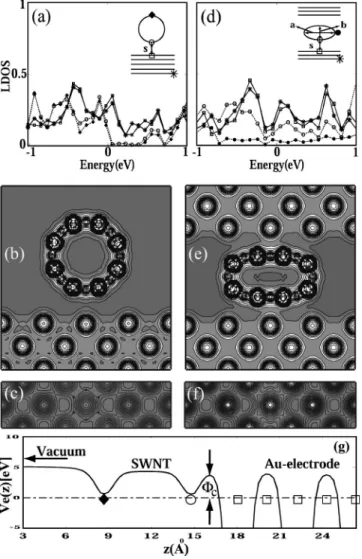
isolated band. The effect on the electronic structure can be revealed for the local density of state 共LDOS兲 calculations. The LDOS calculated for two Au atoms at different sites 共one is at the contact just below the SWNT hexagon; the second being farthest to SWNT mimics the clean Au surface兲 in Fig. 1共a兲 have finite state density at the Fermi level. These two LDOS are similar—there are only minute changes; whereas the LDOS of the carbon atoms at the contact still has a band gap. The Fermi level lies near the top of the valence band of SWNT and complies with a small⌽Bin the hole-doping picture. The LDOS at the carbon atom which is farthest from the metal electrode displays a state distribution similar to that of the carbon atom at the contact region. Cal-culated total charge density of SWNT bonded to the metal electrode, E; that is, 关SWNT⫹E兴, and difference charge density, ⌬⫽关SWNT⫹E兴⫺关E兴⫺关SWNT兴, shows minute charge rearrangement. These results indicate that the weak Au-electrode–SWNT interaction does not induce
sig-nificant changes in the electronic structure. The SCF elec-tronic potential between SWNT and Au electrode, Ve(r)
⫽Vion(r)⫹VH(r)⫹Vx(r), is presented on a vertical plane
and also on a horizontal plane bisecting s in Figs. 1共a兲 and 1共b兲. The shaded area shows that the electronic potential en-ergy at the contact yields a potential barrier ⌽c⫽Ve⫺EF
⬎0. At the contact midway between the SWNT and the Au共100兲 surface ⌽c is calculated to be ⬃3.9 eV, that is
comparable with the calculated work function (⌽⬃5 eV) of the Au slab. Figure 1共g兲 shows the variation of Ve(z) on a
line passing through the center of the SWNT and perpen-dicular to the Au共100兲 surface. The effective potential barrier ⌽c,eff can be even higher owing to the increased
confine-ment of electrons at the contact region. Therefore, electrons that are transferred from the metal to the semiconducting SWNT has to tunnel a potential barrier⌽c,eff(r).
By pressing the s-SWNT between two Au slabs, hence by imposing a radial deformation on the tube关see the inset in Fig 1共d兲兴, we examined the electronic structure and the con-tact potential. Normally, the semiconducting tubes undergo an insulator–metal transition, since the *-singlet states in the conduction band are lowered because of increased * ⫺* hybridization at the high curvature site and eventually overlap with the valence band.9–11In the present case, at a radial deformation, ⑀r⫽b/a⫽0.47, the state density of
SWNT⫹electrode system near EFhas increased partly due to increased state density of the metallized s-SWNT. The spacing s has decreased to 2.6 Å, and eventually potential barrier has collapsed 共i.e., Ve⬍EF) at specific sites at the
contact关see Figs. 1共e兲 and 1共f兲兴. Under these circumstances, the electron from the SWNT can be ballistically transferred to the gold electrodes.
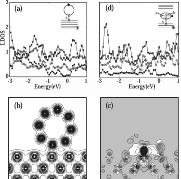
This situation is, however, different in the case of s-SWNT side-bonded to the Mo共110兲 surface, as shown in Fig. 2共a兲. Upon relaxation, the tube has rotated slightly so that C atoms tend to approach to Mo atoms. The interaction energy Ei has been calculated to be⬃3.5 eV. The LDOS at the Mo atom interacting with the C atoms of the SWNT is different from that at the clean Mo共110兲 surface. Moreover, the LDOS at the carbon atom closest to the Mo surface has a finite state density at EF. In particular, the peak near EF is
associated with the C–Mo bond states and hence may be identified as the metal-induced gap states 共MIGS兲. The LDOS of the C atoms farthest from the contact has a band gap near EF. This situation indicates that the site of SWNT
forming contact is conducting, while the opposite site far-thest from the contact remains semiconducting. Owing to the strong Mo–C bond, the spacing between SWNT and Mo electrode is smaller (s⫽1.96 Å) than that with the Au elec-trode. The strong C–Mo bond formation is clarified by the calculated total SCF charge density in Fig. 2共b兲. The differ-ence charge density⌬ presented on a vertical plane in Fig. 2共c兲 shows the strong charge transfer to the C–Mo bonds. The electronic potential calculated on the horizontal plane bisecting s and also on a line from the SWNT to the Mo共110兲 surface through the contact show that Ve(r)⬍EFat the
con-tact region. Accordingly, a potential barrier⌽cdoes not form
at the extended contact between the SWNT-Mo electrode. The radial deformation on the s-SWNT induced by squeez-ing it between two Mo共110兲 electrodes gives rise to the
met-FIG. 1. 共a兲 LDOS at different Au and C atoms of the 共8,0兲 zigzag SWNT side-bonded to the Au共100兲 surface. The location of atoms are described by inset. The zero of energy is taken at the Fermi energy EF. State densities shown by empty circle and filled diamonds correspond to six neighboring carbon atoms. Other densities are for single atoms.共b兲 Contour plots of the SCF electronic potential, Ve(r), on a vertical plane.共c兲 Same as in 共b兲 on a horizontal plane bisecting s. In the dark gray regions Ve(r)⬎EF.共d兲, 共e兲, and共f兲 correspond to the radially deformed 共8,0兲 SWNT pressed between two three-layer Au共100兲 slabs with b/a⫽0.47 as shown by inset. State den-sities shown by empty circles in共d兲 correspond to six neighboring carbon atoms. Other densities are for single atoms. 共g兲 Variation of Ve(z) on a perpendicular line passing through the center of SWNT.
3181
allization of the tube and hence to the increase of state den-sity at EF.
It appears that these results distinguish two different types of electronic structure for two different electrodes. A large spacing and sizable potential barrier between the tube and metal electrode, ⌽c⬃3.9 eV, are characteristics of the contact made with the Au surface. This explains why the devices made from Au electrodes have high contact resis-tance. Here, weak coupling of electronic states cannot lead to MIGS, and the共8,0兲 SWNT is identified to be semiconduct-ing even after the contact has been set with the Au surface. Because of weak coupling and hence finite ⌽c, the
s-SWNT–Au contact is reminiscent of the metal-oxide– semiconductor junction. A small ⌽B is estimated for the
p-type character. Upon radial deformation, s decreases and
eventually⌽ccollapses. Similar features have been observed
recently in scanning tunneling microscopy studies using a
multiwalled carbon nanotube tip and Au共111兲 sample.12 However, ⌽c has disappeared due to strong coupling
be-tween the states of s-SWNT and Mo共110兲.13 The height of the Schottky barrier ⌽B that forms at the SWNT-Mo共110兲
junction having a finite contact region followed by a free s-SWNT depends on the position where the Fermi level is pinned in the gap of s-SWNT. A crude estimate based on the LDOS suggests that ⌽B⬃0.4 eV for the p-type character.
The small cross section of the tube does not allow us to identify a band diagram across the diameter. However, the bands are normally bent along the axis of the s-SWNT and the height of the barrier is monitored by the applied gate voltage. Finally, we note that the electronic properties of present metal–SWNT junctions, in particular the Fermi level pinning exhibits marked differences from those of metal–Si heterostructures, which are known to be insensitive to the type of metal.
This work was partially supported by the National Science Foundation under Grant No. INT01-15021 and TU¨ BI´TAK under Grant No. TBAG-U/13共101T010兲. One of the authors共S.C.兲 acknowledges partial support from Acad-emy of Science of Turkey.
1S. J. Tans, A. R. M. Verscheuren, and C. Dekker, Nature共London兲 393, 49 共1998兲; A. Bachtold, P. Hadley, T. Nakanishi, and C. Dekker, Science 294, 1317共2001兲; T. Nakanishi, A. Bachtold, and C. Dekker, Phys. Rev. B 66, 073307共2002兲.
2H. T. Soh, C. Quate, A. F. Morpurgo, C. M. Marcus, J. Kong, and H. Dai, Appl. Phys. Lett. 75, 627共1999兲; C. Zhou, J. Kong, and H. Dai, ibid. 76, 1597共2000兲.
3R. Martel, V. Derycke, C. Lavoie, J. Appenzeller, K. K. Chan, J. Tersoff, and Ph. Avouris, Phys. Rev. Lett. 87, 256805 共2001兲; Ph. Avouris, R. Martel, V. Derycke, and J. Appenzeller, Physica B 323, 6共2002兲. 4
A. Rochefort, M. Di Vientra, and P. Avouris, Appl. Phys. Lett. 78, 2521 共2001兲.
5S. Heinze, J. Tersoff, R. Martel, V. Derycke, J. Appenzeller, and Ph. Avouris, Phys. Rev. Lett. 89, 106801共2002兲.
6
M. C. Payne, M. P. Teter, D. C. Allen, T. A. Arias, and J. D. Joannopoulos, Rev. Mod. Phys. 64, 1045共1992兲.
7J. P. Perdew and Y. Wang, Phys. Rev. B 46, 6671共1992兲.
8E. Durgun, S. Dag, V. K. Bagci, O. Gu¨lseren, T. Yildirim, and S. Ciraci, Phys. Rev. B 67, 201401共R兲 共2003兲.
9
C. Kilic, S. Ciraci, O. Gu¨lseren, and T. Yildirim, Phys. Rev. B 62, 16345 共2000兲.
10O. Gu¨lseren, T. Yildirim, and S. Ciraci, Phys. Rev. Lett. 87, 116802 共2001兲.
11
O. Gu¨lseren, T. Yildirim, S. Ciraci, and C. Kilic, Phys. Rev. B 65, 155410 共2002兲; O. Gu¨lseren, T. Yildirim, and S. Ciraci, ibid. 65, 153405 共2002兲. 12M. Luna, P. J. de Pablo, J. Colchero, J. Gomez-Herrero, A. M. Baro, H.
Tokumoto, and S. P. Jarvis, Ultramicroscopy 96, 83共2003兲.
13E. Tekman and S. Ciraci, Phys. Rev. B 43, 7145共1991兲; S. Ciraci, in Scanning Tunneling Microscopy III, edited by R. Wiesendanger and H.-J. Gu¨ntherodt共Springer, Berlin, 1993兲.
FIG. 2. 共a兲 LDOS at different Mo and C atoms of the 共8,0兲 zigzag SWNT side-bonded to the Mo共110兲 surface. The location of atoms are described by inset. The zero of energy is taken at the EF. State densities shown by empty circles and filled diamond correspond to eight neighboring carbon atoms, Others are for single atoms.共b兲 Contour plots of the total SCF charge den-sity on a vertical plane.共c兲 Difference charge density showing the charge depleted共white兲 regions and charge accumulate 共black兲 regions. 共d兲 LDOS corresponding to the共8,0兲 SWNT radially deformed between two three-layer Mo共110兲 slabs with b/a⫽0.56 as shown by the inset. State densities shown by empty circles correspond to 10 neighboring carbon atoms.