Fabrication, modeling and characterization of GaN HEMTs, and design of high power MMIC amplifiers
177
0
0
Tam metin
(2) I certify that I have read this thesis and that in my opinion it is fully adequate, in scope and in quality, as a thesis for the degree of Master of Science.. Prof. Dr. Ekmel Özbay (Supervisor). I certify that I have read this thesis and that in my opinion it is fully adequate, in scope and in quality, as a thesis for the degree of Master of Science.. Prof. Dr. Abdullah Atalar. I certify that I have read this thesis and that in my opinion it is fully adequate, in scope and in quality, as a thesis for the degree of Master of Science.. Assoc. Prof. Dr. Oğuz Gülseren. Approved for the Institute of Engineering and Sciences:. Prof. Dr. Mehmet B. Baray Director of Institute of Engineering and Sciences. ii.
(3) ABSTRACT FABRICATION, MODELING AND CHARACTERIZATION OF GaN HEMTs, AND DESIGN OF HIGH POWER MMIC AMPLIFIERS Muhammed A. ACAR M.S. in Electrical and Electronics Engineering Supervisor: Prof. Dr. Ekmel ÖZBAY November 2009. High power and high frequency requirements in advanced telecommunication systems become more stringent as faster and higher capacity wireless data transfer over long distances is getting a common need for both military and commercial applications. Present mature semiconductor technologies have already reached their performance limits in responding next generation needs of high power modules. Under these circumstances, further improvements seem to be possible via introducing more capable technology. GaN HEMT device technology promises high power performance in microwave and millimeterwave regimes at least an order of magnitude better than any other current counterparts. Research and development processes of this technology require deep understanding of theoretical fundamentals of HEMT device formation and should be supported by efficient epitaxial wafer growth and microfabrication facilities, and accurate large-signal nonlinear modeling capability. After all, GaN HEMT technology can be transformed to real applications of monolithic microwave integrated circuit (MMIC) power amplifiers (PAs). This work can be separated into three main parts. In the first part, we introduced bottom up approach to the GaN HEMT technology starting from GaN material properties, semiconductor physics and design of GaN HEMT devices, and MOCVD growth and characterization, completing with fabrication. iii.
(4) processes and large-signal nonlinear modeling issues of the active devices. 2DEG sheet carrier concentrations in the order of 1x1013 cm-2 and electron mobility values between 1500-2000 cm2/V·s are obtained from our GaN HEMT epiwafers. Furthermore, 900mA/mm of maximum drain current density, 32GHz of fT, and 40 GHz of fmax are achieved from a fabricated 6x150um GaN HEMT device. Large-signal nonlinear modeling is applied successfully for a 4x200um device with 1um gate length. In the second part, this model is used as a basis for two MMIC PA designs have center frequency of 2GHz and coplanar wave guide passive elements. ~2W and ~4W output power levels and ~42% and ~35% PAE values are generated from these MMIC PAs at 1dB compression point, respectively. In the final part, we applied our MMIC PA design experiences to a GaAs pHEMT process of UMS foundry. We introduced two-stage balanced PA topology in order to achieve wideband and high power response at the output. Aimed frequency range is 18-22GHz. According to the simulation results, output power of ~2W is obtained with 31%-35% PAE in this frequency band. Sparameter measurement data are quite in agreement with simulation results, even better. CW power measurement results are subjected to 1-2dB degradation in output power levels compared to HB simulation results since the design kit we used contains pulsed measurement based transistor models. The measurements results proved the efficiency and correctness of our design.. Keywords:. GaN. HEMT,. MMIC. PA. design,. MOCVD. growth,. microfabrication, large-signal nonlinear modeling, K-band balanced MMIC PA design, GaAs pHEMT.. iv.
(5) ÖZET GaN HEMT YAPILARININ ÜRETĐMĐ, MODELLENMESĐ VE ÖLÇÜMÜ, VE YÜKSEK GÜÇLÜ MMIC YÜKSELTEÇLERĐN TASARIMI Muhammed A. ACAR Elektrik ve Elektronik Mühendisliği Bölümü Yüksek Lisans Tez Yöneticisi: Prof. Dr. Ekmel ÖZBAY Kasım 2009. Daha hızlı ve daha yüksek kapasiteli uzun mesafe kablosuz veri iletimi, askeri ve sivil uygulamalarda yaygın bir ihtiyaç haline geldikçe; ileri düzey telekomunikasyon sistemlerindeki yüksek güç ve yüksek frekans gereksinimleri çok daha zor ulaşılabilir hale gelmiştir. Günümüzün gelişimini tamamlamış yarıiletken teknolojileri, yüksek güç birimlerinde belirlenen ihtiyaçları karşılama noktasında kendi limitlerine ulaşmış durumdadır. Bu koşullarda, bahsedilen sorunların çözümü ve daha ileri hedeflerin gerçekleştirilmesi ancak daha yüksek kapasiteli bir teknoloji aracılığı ile mümkün görülmektedir. GaN HEMT aygıt teknolojisi mikrodalga ve milimetre dalga frekanslarinda diğer eşdeğer teknolojilere kıyasla en az 10 kat daha fazla çıkış güç performansı vaadetmektedir. Bu teknolojinin araştırma geliştirme süreci, HEMT aygıt oluşumu altında yatan fiziksel prensiplere çok iyi derecede hakim olmayı gerektirmektedir; yine bu sürecin, elverişli epitaksiyel yapı büyütme ve mikrofabrikasyon ekipmanları, ve yüksek doğruluk derecesinde büyük-işaret modelleme becerileri ile desteklenmesi gerekmektedir. Bu şartlar yerine getirilip GaN HEMT. teknolojisi oluşturulduktan. sonra MMIC güç. yükselteç. uygulamaları gerçekleştirilebilir. Bu çalışma üç ana başlık altında toplanabilir. Đlk kısımda, GaN malzeme özellikleri, GaN HEMT aygıtların yarıiletken fiziği ve epitaksiyel tasarımı,. v.
(6) MOCVD büyütme ve karakterizasyonu, mikrofabrikasyon adımları ve büyük işaret modelleme konuları ele alınarak, GaN HEMT teknolojisine en temelden başlayan ve sonuç olarak modeli çıkarılmış aktif aygıt noktasına kadar inceleyen bir yaklaşım ortaya konmuştur. GaN HEMT epitaksiyel yapılarımızda tipik olarak, iki boyutlu elektron gazı (2DEG) taşıyıcı yoğunluğu 1x1013 cm-2 mertebesinde ve elektron mobilitesi değerleri 1500 ila 2000 cm2/V·s arasında elde edilmiştir. Fabrikasyonu tamamlanmış 6x150um’luk bir GaN HEMT aygıtında, 900mA/mm maksimum drain akım yoğunluğu, 32GHz fT, ve 40GHz fmax değerlerine ulaşılmıştır. Kapı uzunluğu 1um olan 4x200um’luk bir aygıtın büyük-işaret modeli başarılı bir şekilde elde edilmiştir. Đkinci kısımda, çıkarılan bu model, merkez frekansı 2GHz olan ve coplanar dalga kılavuzu yapısında pasif elemanlar içeren iki çeşit MMIC güç yülselteci tasarımında kullanılmıştır. Bu tasarımlarda 1dB kompresyon noktasında sırasıyla, ~2W ve ~4W çıkış gücü, ve ~%42 ve ~%35 güç katkılı verim (PAE) değerleri oluşturulmuştur. Son kısımda, tasarım tecrübelerimizi UMS firmasının GaAs pHEMT tasarım kitini kullanarak uygulamaya geçirdik. Hedeflenen geniş bant (18-22GHz) ve yüksek güç kapasitesine ulaşabilmek için iki aşamalı dengeli güç yükselteç topolojisi kullanılmıştır. Simulasyon sonuçlarına göre bu frekans bandında, yaklaşık 2W çıkış gücü ve %31 ila %35 arasında değişen PAE değerleri elde edilmiştir. Küçük işaret ölçümleri simulasyonlarla oldukça uyum içerisinde çıkmış hatta daha iyi sonuçlar vermiştir. CW çıkış gücü ölçüm sonuçları HB simulasyon sonuçlarının 1-2dB civarında altında kalmıştır. Bu durumun nedeni ise kullanılan tasarım kitinin atmalı ölçümlere dayalı transistor modelleri içermesidir. Ölçümler sonucunda yapılan MMIC PA tasarımının etkinliği ve doğruluğu ortaya konmuştur. Anahtar kelimeler: GaN HEMT, MMIC PA tasarımı, MOCVD büyütme, mikrofabrikasyon, büyük-işaret modelleme, K-bant dengeli MMIC PA tasarımı, GaAs pHEMT.. vi.
(7) Acknowledgements I would like to thank my supervisor Prof. Ekmel Özbay, for his great support and encouragement during the course of this work. It was an honor and a remarkable experience to participate in various advanced projects under his invaluable guidance. I would also like to express my deepest gratitude to Prof. Abdullah Atalar and Dr. Tarık Reyhan for their invaluable comments and advices on my MMIC PA designs. I learned a lot from their immense experiences. I am also grateful to Assoc. Prof. Oğuz Gülseren for reviewing this thesis. I am thankful to Mustafa Öztürk, Başar Bölükbaş, Özgür Kelekçi, Bayram Bütün, Kamil Bora Alıcı, and other NANOTAM and BilUzay members for their generous helps and favorable discussions which form the critical milestones of this work. Financial support of The Scientific and Technological Research Council of Turkey (TÜBĐTAK) related to the National Scholarship Programme for MSc Students is cordially acknowledged. Finally, my very special thanks belong to my sweetheart, my future wife, Sevgi, for making my life meaningful and enjoyable. Without her deep understanding, endless discretion and boundless love, I wouldn’t be able to take any progress in my challenging studies. I hereby dedicate this labor to my soulmate.. vii.
(8) Table of Contents ABSTRACT ...................................................................................... III ÖZET .................................................................................................V ACKNOWLEDGEMENTS .......................................................................VII TABLE OF CONTENTS ........................................................................VIII LIST OF FIGURES ..................................................................................X LIST OF TABLES .............................................................................. XVII 1. INTRODUCTION ............................................................................... 1 2. GAN HIGH ELECTRON MOBILITY TRANSISTORS .................. 8 2.1 GAN MATERIAL PROPERTIES ......................................................... 8 2.2 PRINCIPLE OF GAN HEMTS ......................................................... 14 2.3 EPITAXIAL STRUCTURE ................................................................ 20 2.4 MOCVD GROWTH....................................................................... 28 2.5 WAFER CHARACTERIZATION ........................................................ 35 3. FABRICATION TECHNOLOGY AND CHARACTERIZATION OF HEMTS........................................................................................ 44 3.1 MASK DESIGN.............................................................................. 44 3.2 LITHOGRAPHY TECHNIQUES USED ................................................ 47 3.3 METALLIZATION TECHNIQUES USED............................................. 53 3.4 FABRICATION STEPS ..................................................................... 56 3.5 CHARACTERIZATION OF THE FABRICATED GAN HEMTS ............... 69 4. COMPACT MODELING ISSUES OF HEMT DEVICES .............. 76 4.1 SMALL-SIGNAL LINEAR MODELING OF HEMTS ............................ 77 4.2 LARGE-SIGNAL NONLINEAR MODELING OF HEMT DEVICES ......... 80. viii.
(9) 4.3 LARGE-SIGNAL NONLINEAR MODEL EXTRACTION OF OUR GAN HEMT USING TOPAS SOFTWARE ..................................................... 83 4.4 VALIDATION OF THE LARGE-SIGNAL NONLINEAR GAN HEMT MODEL.............................................................................................. 89 5. 2GHZ GAN HEMT COPLANAR MMIC POWER AMPLIFIER DESIGNS ........................................................................................... 98 5.1 PA DESIGN CONSIDERATIONS ...................................................... 98 5.2 COPLAN SOFTWARE FOR CPW DESIGN .................................... 102 5.3 GAN HEMT CPW MMIC PA DESIGN STEPS ............................. 104 5.4 SIMULATION RESULTS OF THE MMIC PA DESIGNS ..................... 110 6. K-BAND GAAS PHEMT BALANCED MMIC POWER AMPLIFIER DESIGN .................................................................... 118 6.1 FOUNDRY SERVICE..................................................................... 120 6.2 K-BAND DESIGN CONSIDERATIONS ............................................. 123 6.3 LANGE COUPLER DESIGN ........................................................... 131 6.4 SIMULATION AND MEASUREMENT RESULTS OF THE K-BAND BALANCED MMIC PA..................................................................... 138 7. SUMMARY & FUTURE WORK ................................................... 149 APPENDIX-A ................................................................................... 151 APPENDIX-B.................................................................................... 152 BIBLIOGRAPHY........................................................................... 154. ix.
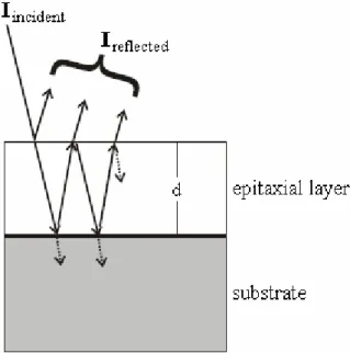
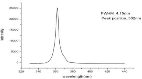
(10) List of Figures Figure 1.1 Cross section (a) and band diagram (b) of GaAs HEMT Structure. 2 Figure 2.1 Schematic illustration of GaN wurtzite crystal structure. The blue and green spheres indicate Ga and N, respectively. GaN with Ga-face polarity is shown on the top and GaN with N-face polarity is shown on the bottom of the figure. ....................................................................... 11 Figure 2.2 Spontaneous polarization fields and sheet charges occurred in GaN and AlGaN grown in [0001] direction................................................... 12 Figure 2.3 Piezoelectric polarization field and sheet charges in AlGaN layer.13 Figure 2.4 Illustration of piezoelectric and spontaneous polarization fields and sheet charges in AlGaN/GaN structure.................................................. 14 Figure 2.5 Basic GaN HEMT structure......................................................... 14 Figure 2.6 Band diagram of the AlGaN/GaN heterostructure and accumulated sheet charges in the system. .................................................................. 17 Figure 2.7 Illustration of surface donor model. ............................................. 19 Figure 2.8 Sample epilayer structure with low temperature AlN nucleation layer. .................................................................................................... 23 Figure 2.9 Conduction band profiles with and without a GaN cap layer. ....... 26 Figure 2.10 Epilayer structure with surface passivation layer of Si3N4. ......... 28 Figure 2.11 AIXTRON RF200/4 RF-S MOCVD system. ............................. 29 Figure 2.12 Reactor of the MOCVD system in NANOTAM......................... 29 Figure 2.13 Optimized epitaxial design of AlGaN/GaN HEMTs on sapphire. ............................................................................................................. 30 Figure 2.14 Illustration of incident and reflected beams of the optical reflectance measurements. .................................................................... 32. x.
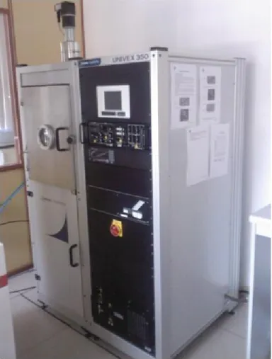
(11) Figure 2.15 Optical reflectance graphs of B-1540 wafer. .............................. 32 Figure 2.16 Optical reflectance graphs of B-1545 wafer. .............................. 34 Figure 2.17 Photograph of Jobin Yvon Triax 550ccd Photoluminescence System in NANOTAM. ........................................................................ 35 Figure 2.18 PL measurement graph of GaN layer of the B-1545 epiwafer. ... 36 Figure 2.19 Ocean Optics USB4000-UV-VIS and USB-ISS-UV-VIS modules. ............................................................................................................. 36 Figure 2.20 Optical transmission measurement of AlGaN barrier layer......... 37 Figure 2.21 Photograph of Veeco di CP-II multi mode AFM system in NANOTAM. ........................................................................................ 38 Figure 2.22 Contact-mode AFM scan graph of B-1545 epiwafer. ................. 38 Figure 2.23 EGK HEM-2000 Hall Effect measurement system in NANOTAM. ........................................................................................ 39 Figure 2.24 Illustration of a sample prepared for Hall Effect measurement. .. 40 Figure 2.25 Hall Effect measurements of B-1540 epiwafer. .......................... 42 Figure 2.26 Hall Effect measurements of B-1545 epiwafer. .......................... 43 Figure 3.1 HEMT photo-mask layout. .......................................................... 46 Figure 3.2 An 8x75µm HEMT layout........................................................... 47 Figure 3.3 Spin-coating steps........................................................................ 48 Figure 3.4 SCS Spincoat System. ................................................................. 48 Figure 3.5 Illustration of mask alignment scenarios. ..................................... 49 Figure 3.6 Photo of a Karl Suss MA6 Mask Aligner System......................... 50 Figure 3.7 Schematic illustration of negative (a) and positive (b) photolithography. ................................................................................. 50 Figure 3.8 Steps of etch-back process. .......................................................... 51 Figure 3.9 Steps of lift-off process................................................................ 52 Figure 3.10 Photo of an E-beam lithography system. .................................... 53 Figure 3.11 Photo of the Leybold Univex 350 E-beam evaporator in NANOTAM. ........................................................................................ 54 Figure 3.12 Schematic of our Au electroplating setup................................... 55. xi.
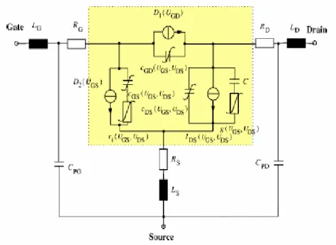
(12) Figure 3.13 Schematic illustration (a) and a photo (b) of the sample after mesa etching step. ......................................................................................... 57 Figure 3.14 Schematic illustration (a) and photos of the Ohmic contacts before (b) and after (c) the annealing process................................................... 59 Figure 3.15 Photo of the SSI Solaris 75 RTP system in NANOTAM. ........... 60 Figure 3.16 RTP temperature vs. time graph................................................. 60 Figure 3.17 Schematic illustration of the TLM pattern.................................. 61 Figure 3.18 TLM measurement data and corresponding graph...................... 61 Figure 3.19 Band diagrams of a metal and a semiconductor (a) and Schottky contact after connection (b)................................................................... 62 Figure 3.20 Schematic illustration (a) and photos (b-c) of the device after gate metallization. ........................................................................................ 63 Figure 3.21 Schematic illustration of virtual gate formation in GaN HEMT devices. ................................................................................................ 64 Figure 3.22 An air-bridge post profile before (a) and after (b) reflow process. ............................................................................................................. 65 Figure 3.23 Some device photos after the air-bridge post step....................... 66 Figure 3.24 Photo of a device after the seed layer removal step. ................... 67 Figure 3.25 SEM photos of the fabricated air-bridges. .................................. 68 Figure 3.26 A photo of a fabricated HEMT device taken by microscope....... 69 Figure 3.27 Schematic view of our DC characterization setup. ..................... 70 Figure 3.28 A typical DC-IV graph of GaN HEMT device. .......................... 70 Figure 3.29 DC characterization results of a 6x150µm GaN HEMT device. . 72 Figure 3.30 DC characterization results of a 4x150µ m GaN HEMT device. . 72 Figure 3.31 Schematic view of an AC measurement setup............................ 73 Figure 3.32 Current gain (a) and unilateral power gain (b) graphs of a 6x150µm GaN HEMT. ......................................................................... 75 Figure 3.33 Current gain (a) and unilateral power gain (b) graphs of a 4x150µm GaN HEMT. ......................................................................... 75 Figure 4.1 The bias dependent small-signal equivalent circuit of the HEMT device. .................................................................................................. 77. xii.
(13) Figure 4.2 Summary of extrinsic element extraction procedure, and corresponding EECs under (a) “pinched-cold” and (b) “gate forward cold” conditions.................................................................................... 78 Figure 4.3 Steps of extrinsic elements de-embedding.................................... 79 Figure 4.4 The large-signal electrical equivalent circuit of the HEMT device. ............................................................................................................. 82 Figure 4.5 Schematic illustration of the single-pulse type measurement setup in IMST GmbH. ................................................................................... 84 Figure 4.6 Photo of the Rohde & Schwarz ZVA high speed VNA used in IMST GmbH ........................................................................................ 85 Figure 4.7 Screenshot of the extrinsic element optimization window on TOPAS................................................................................................. 86 Figure 4.8 Screenshot of the intrinsic elements settings window on TOPAS. 87 Figure 4.9 Output I-V Curves of the modeled GaN HEMT........................... 89 Figure 4.10 Comparison of measured (red curves) and simulated (blue curves) (using nonlinear TOPAS model) S-parameters at bias point “m1” (VGS=0V, VDS=4V). .............................................................................. 90 Figure 4.11 Comparison of measured (red curves) and simulated (blue curves) (using nonlinear TOPAS model) S-parameters at bias point “m2” (VGS=1.5V, VDS=1.5V)................................................................................... 91 Figure 4.12 Comparison of measured (red curves) and simulated (blue curves) (using nonlinear TOPAS model) S-parameters at bias point “m3” (VGS=3V, VDS=3V)......................................................................................... 92 Figure 4.13 Comparison of measured (red curves) and simulated (blue curves) (using nonlinear TOPAS model) S-parameters at bias point “m4” (VGS=2V, VDS=12V)....................................................................................... 93 Figure 4.14 Comparison of measured (red curves) and simulated (blue curves) (using nonlinear TOPAS model) S-parameters at bias point “m5” (VGS=2V, VDS=17V)....................................................................................... 94. xiii.
(14) Figure 4.15 Comparison of measured (red curves) and simulated (blue curves) (using nonlinear TOPAS model) S-parameters at bias point “m6” (VGS=5.5V, VDS=20V).................................................................................... 95 Figure 4.16 Output power and power gain comparisons between our GaN HEMT “pulsed” large-signal model and CW power measurements....... 97 Figure 5.1 Important properties of various PA classes of operation............... 99 Figure 5.2 Illustration of input and output signals and load line for Class A PA. ..................................................................................................... 100 Figure 5.3 Basic schematic of single stage amplifier................................... 101 Figure 5.4 Broadband equivalent circuit model of coplanar spiral inductor implemented in COPLAN software. ................................................... 103 Figure 5.5 Modeling steps of coplanar structures used in COPLAN software. ........................................................................................................... 103 Figure 5.6 Load-pull simulation result of our GaN HEMT model. .............. 104 Figure 5.7 Source-pull simulation result of our GaN HEMT model. ........... 105 Figure 5.8 GBN layout of the first design. .................................................. 106 Figure 5.9 S-parameter simulation results of the GBN. ............................... 106 Figure 5.10 DBN layout of the first design. ................................................ 106 Figure 5.11 S-parameter simulation results of the DBN. ............................. 107 Figure 5.12 Schematic of the first CPW GaN HEMT MMIC PA. ............... 107 Figure 5.13 Layout of the first CPW GaN HEMT MMIC PA. .................... 108 Figure 5.14 Schematic of the second CPW GaN HEMT MMIC PA............ 108 Figure 5.15 Layout of the second CPW GaN HEMT MMIC PA................. 109 Figure 5.16 Power gain (red) and output power (blue) vs. input power sweep for the first design............................................................................... 111 Figure 5.17 PAE vs. Input power sweep for the first design. ....................... 111 Figure 5.18 Forward transmission (S21) of the first design. ........................ 112 Figure 5.19 Input and output matching of the first design. .......................... 113 Figure 5.20 Stability factor of the first design. ............................................ 113 Figure 5.21 Power gain (red) and output power (blue) vs. input power sweep for the second design. ......................................................................... 114. xiv.
(15) Figure 5.22 PAE vs. input power sweep for the second design.................... 115 Figure 5.23 Forward transmission (S21) of the second design..................... 115 Figure 5.24 Input and output matching of the second design....................... 116 Figure 5.25 Stability factor of the second design......................................... 117 Figure 6.1 Block diagram of the balanced MMIC PA design. ..................... 119 Figure 6.2 Typical UMS foundry service steps in order. Steps surrounded with dashed lines are optional. .................................................................... 121 Figure 6.3 Load-pull simulation result of an 8x125um UMS GaAs pHEMT device. ................................................................................................ 124 Figure 6.4 Source-pull simulation result of an 8x125um UMS GaAs pHEMT device. ................................................................................................ 124 Figure 6.5 Layout of on chip MIM by-pass capacitor with via hole............. 126 Figure 6.6 S-parameter simulation results of the shunt by-pass capacitor. ... 126 Figure 6.7 Schematic of the single branch of our balanced MMIC PA. ....... 128 Figure 6.8 Layout of the single branch of our balanced MMIC PA. ............ 129 Figure 6.9 Layout of the Momentum test structure...................................... 130 Figure 6.10 S-parameter comparison of schematic and Momentum simulations of the test structure with 5 ports. ......................................................... 131 Figure 6.11 Typical Lange coupler geometry with four fingers................... 132 Figure 6.12 First draft layout of the Lange coupler ..................................... 133 Figure 6.13 Various simulation results of the S-parameter magnitudes at direct and coupled ports................................................................................ 134 Figure 6.14 Various simulation results of the S-parameter phase values at direct and coupled ports...................................................................... 134 Figure 6.15 Final layout of the Lange coupler............................................. 135 Figure 6.16 Momentum simulation results of the final Lange coupler design ........................................................................................................... 136 Figure 6.17 Final layout of the K-band GaAs pHEMT balanced MMIC PA. ........................................................................................................... 137 Figure 6.18 S-parameter simulation results of the single branch two-stage MMIC PA. ......................................................................................... 138. xv.
(16) Figure 6.19 Layout of the DC board of the MMIC chip. ............................. 139 Figure 6.20 Photo of our S-parameter measurement setup. ......................... 140 Figure 6.21 Gain comparison between measurements and simulations........ 141 Figure 6.22 I/O Reflection comparison between measurements and simulations. ........................................................................................ 141 Figure 6.23 Reverse isolation comparison between measurements and simulations. ........................................................................................ 142 Figure 6.24 Stability factor comparison between measurements and simulations. ........................................................................................ 142 Figure 6.25 Photo of our CW power measurement setup. ........................... 143 Figure 6.26 HB simulation results of our MMIC chip under 16dBm input signal level. ........................................................................................ 144 Figure 6.27 Power dissipation at input and output Lange coupler 50 Ohm resistors. ............................................................................................. 144 Figure 6.28 Output power and power gain simulation and measurement results at 18GHz. ........................................................................................... 145 Figure 6.29 Output power and power gain simulation and measurement results at 20GHz. ........................................................................................... 145 Figure 6.30 Output power and power gain simulation and measurement results at 22GHz. ........................................................................................... 146 Figure 6.31 Microscope image of the GaAs MMIC PA chip....................... 147 Figure 6.32 Photo of the MMIC chip on the DC board under probe station. 148 Figure 6.33 100pF single layer by-pass capacitors next to the MMIC chip.. 148. xvi.
(17) List of Tables Table 1.1 GaN-based micro-electronics applications. ..................................... 3 Table 1.2 Important figures-of-merit for GaAs, 4H-SiC, 6H-SiC and GaN relative to Si. .......................................................................................... 4 Table 2.1 Important material properties of selected semiconductors. .............. 9 Table 2.2 c0/a0 ratio and spontaneous polarization values of wurtzite crystal GaN and AlN........................................................................................ 12 Table 2.3 Required material properties of GaN and AlN for 2DEG calculations........................................................................................... 15 Table 6.1 Important properties of UMS processes....................................... 122. xvii.
(18) Chapter 1 Introduction Invention of the solid-state transistor, in 1947, became a major milestone in evolution of modern electronics since transistor is the inevitable key component of almost all electronic circuits. Later on, semiconductor technology has been increasingly improved to achieve mass production and higher capacity transistors. Today, this trend still continues to have faster, powerful and reliable transistors. To do so, people try to explore and study on new material systems rather than conventional mature technologies. One might ask why we need better transistors and say just be contented with today’s mature technology since it is safe and cheap. There are two answers to this question, first one is logical and second one is technical. Logical one is that we wouldn’t able to reach current mature technology if newer materials and technologies were not studied. In order to figure out the technical answer let’s consider an explanatory example, that is telecommunication. Need for telecommunication is apparent since without it no one can configure and reestablish. needs. of. humanity. in. modern. world.. Usage. area. of. telecommunication covers everything from civil to military applications and transistor quality determines the limits of the telecommunication capacity. If we develop higher performance transistors, we can reduce the product volumes and weights,. and. built. up. more. energy. efficient. and. more. reliable. telecommunication systems compared to previous technologies. All these mean that we will achieve safer and cheaper electronic equipments.. 1.
(19) Micro-electronics has been evolved with the usage of Germanium (Ge), Silicon (Si), Silicon Germanium (SiGe), and Gallium Arsenide (GaAs) semiconductor materials. In 1979, invention of the GaAs high electron mobility transistors (HEMTs) was very important breakpoint in the near electronics history [1]. Very high sheet carrier densities and mobility values were achieved with this invention. GaAs HEMT structure is basically formed by a non-doped GaAs channel layer and a highly doped n-type AlGaAs donor-supply layer. This heterojunction of different band-gap materials constitutes a triangular-like quantum well on the GaAs side of the conduction band which allows electrons move freely parallel to the heterojunction plane without any impurity collision. This collection of high mobility electrons inside the quantum well is called two dimensional electron gas (2DEG). Basic epitaxial structure and band diagram of GaAs HEMT are shown in Figure 1.1a and Figure 1.1b, respectively. GaAs HEMT technology has reached its mature state after many improvements in the epitaxial structure and material quality. HEMT structure was transferred to Gallium Nitride (GaN) material system in order to seek for higher performance transistors.. Figure 1.1 Cross section (a) and band diagram (b) of GaAs HEMT Structure.. 2.
(20) GaN, which is wide band-gap III-V compound, is the latest semiconductor that has been extensively studied on for high power applications. In 1994, first AlGaN/GaN high electron mobility transistor (HEMT) is demonstrated by Khan et al. [2]. Researches on GaN indicate very promising results compared to other semiconductor technologies. This improvement belongs to the superior material properties of AlGaN/GaN material system. GaN HEMT structure is investigated comprehensively throughout next chapter. Table 1.1 lists fundamental application areas of GaN technology. Application. Field RF Power Transistors. Wireless Base Stations. High Frequency MMICs. Wireless Broadband Access. Military. Radar/Communication Links. Power Transmission Lines. High Voltage Electronics. Power Conditioning. Mixed-signal Integration. Switches. Plasma Display Panels. High-temperature Sensors. Engine Electronics. Hall Sensors. Automotive Applications. MEMS. Pressure Sensors Table 1.1 GaN-based micro-electronics applications.. We focused on high power characteristics of transistors in this thesis. GaN is known to be the most suitable semiconductor for high power applications compared to other materials. Some figures-of-merit have been proposed to quantify the performance limits of the materials using their important parameters related to specific applications. Keyes’ figure-of-merit describes the thermal limitations for switching behavior of high speed transistors used in integrated circuits. High frequency and high power operation capability of a material is estimated by Johnson’s figure of merit. Baliga high-frequency figure of merit. 3.
(21) predicts switching power loss of a material at high frequency. Baliga figure-ofmerit defines the capacity of having minimum conduction losses in power transistors [3].. Table 1.2 lists Keyes, Johnson, Baliga high-frequency and. Baliga figures-of-merit for Si, GaAs, 4H-SiC, 6H-SiC and GaN materials normalized to Si [4]. As can be seen from these figures-of-merit values, GaN proves its promising high power capacity. Keyes. Johnson. Baliga HF. Baliga. [κ(vsat/εr)1/2]. [(Ecr·vsat/π)2]. [µ n·Ecr2]. [εr·µ n·Ecr3]. Si. 1. 1. 1. 1. GaAs. 0.45. 7.1. 10.8. 15.6. 4H-SiC. 4.61. 180. 22.9. 130. 6H-SiC. 4.68. 260. 16.9. 110. GaN. 1.6. 760. 77.8. 650. Material. Table 1.2 Important figures-of-merit for GaAs, 4H-SiC, 6H-SiC and GaN relative to Si.. Growing IC market and increasing demand for stringent electronic circuit specifications pushed researchers to develop genius, effective and ‘all-in-one’ solution, monolithic microwave integrated circuit (MMIC). In 1975, R. S. Pengelly reported first MMIC which is GaAs FET based low noise amplifier [5]. As the name implies MMICs contain all circuit elements as planar on same substrate without any external interconnections and bonds. This nature of MMICs allows operation of higher frequencies with lower losses and makes it more feasible and reliable compared to previous hybrid technology. In terms of simple integrity to the outer electrical environment, MMICs are internally matched to 50 Ohm in general. Today, MMICs are the fundamental components of the microwave electronic systems e.g. cell phones, WiMAX applications, and satellite transceivers.. 4.
(22) In this work, we pursued the steps of achieving MMIC power amplifiers from bare transistor investigation stage to extensive MMIC design phase. Firstly, GaN HEMT epitaxial structure was designed and grown using metal organic chemical vapor deposition (MOCVD) system. At next stage, transistor layout was defined and fabrication was carried out on epiwafers. Fabricated samples were characterized and selected to be modeled. Since we are interested in high power characteristics, we need nonlinear large signal modeling of transistors. For this purpose we used TOPAS software of IMST GmbH [6]. After obtaining the model of our GaN HEMTs, we designed 2W and 4W coplanar MMIC power amplifiers at 2GHz. Coplanar capacitors, inductors, transmission lines, and junctions were modeled using COPLAN software (from IMST) that is compatible with Advanced Design Software (ADS) [7]. In order to gain further experience in MMIC design at higher frequencies, we used UMS foundry service and designed K-band GaAs pHEMT MMIC balanced power amplifier. Chapter 2 gives the background information on GaN HEMTs. First, GaN material properties and their influence on high power characteristics of GaN HEMTs are described. Then, principle of GaN HEMTs is explained including theory of 2DEG formation. Next, epitaxial structure of GaN HEMT is investigated. Finally, second chapter concludes with the illustration of MOCVD growth details of GaN HEMT structure together with data taken from MOCVD system, and characterization results of grown wafers. Chapter 3 deals with fabrication technology and characterization of GaN HEMTs. First, mask design issue is covered. Then, lithography and metallization techniques which we have used in our fabrication process are explained. Next, GaN HEMT fabrication process is described step by step, namely, mesa etching, Ohmic contact metallization, Ohmic contact annealing, gate metallization using e-beam lithography system, SiN passivation, air-bridge post, seed layer of electroplating, air-bridge metallization, and seed layer. 5.
(23) removal steps. This chapter concludes with the DC and RF characterization results of the fabricated GaN HEMT devices. Chapter 4 starts with describing small signal linear modeling of the HEMT devices, and then continues with representing nonlinear large-signal modeling techniques i.e. physical models, analytical models and table-based models. Next, modeling of GaN HEMTs using TOPAS software (IMST GmbH) is explained. Nonlinear large signal model extraction from S-parameter measurements at multi-bias points is described in detail. Comparison of extracted model and measurement is given and accuracy of the model is discussed. Chapter 5 contains detailed work on coplanar MMIC power amplifier design at 2GHz using our own GaN HEMT model and COPLAN software of IMST GmbH. Description of design methodology is given for two different designs. COPLAN software is investigated deeply in order to understand physical background and use it in more efficient way. Design steps including load pull simulations, DC bias circuits, input & output matching networks are explained. At the end of fifth chapter, simulation results of the designs are shown and commented. Chapter 6 is devoted to K-band GaAs pHEMT MMIC balanced power amplifier design using UMS foundry design kit. First, information about the UMS foundry service is given. Then, balanced design methodology is introduced. Design details and critical considerations are explained. Wideband matching techniques are discussed. Electromagnetic coupling effect is investigated throughout the circuit especially for Lange couplers. 2.5D and 3D EM simulation results of critical parts are given. Simulation results of whole circuit are illustrated. Next, measurement board design for our MMIC is explained. Finally, on wafer measurement data are compared with simulation results.. 6.
(24) Chapter 7 summarizes works done and results obtained in the thesis. Future work vision towards more powerful, efficient and reliable transistors and power amplifiers is described.. 7.
(25) Chapter 2 GaN High Electron Mobility Transistors This chapter provides general physical understanding of GaN high electron mobility transistors (HEMTs) starting from material properties of GaN. Then, principle of GaN HEMT operation including fundamental of two dimensional electron gas (2DEG) formation is given. Next, epitaxial structure behind the HEMT device is examined. Further, MOCVD growth of GaN HEMTs is described and characterization results of epiwafer are illustrated.. 2.1 GaN Material Properties Over the last decades, GaN has been very promising research topic and candidate for high power applications due to its superior material properties over conventional ones. Important material properties of GaN and some other semiconductors are listed in Table 2.1. GaN is a wide band-gap material so that it can stand at extreme environmental conditions such as high temperatures and voltages [8], [9], [10], [11]. Radiation hardness of the GaN is comparable with SiC and higher than GaAs [12]. This fact makes GaN very attractive for space applications. Thermal conductivity of GaN is significantly higher than that of GaAs. This is another measure that makes GaN more suitable for high power operation needs compared to GaAs power devices. Furthermore, saturated. 8.
(26) electron drift velocity of GaN is higher than that of Si, SiC and GaAs. This puts GaN into better position for high saturation current and high frequency applications compared to its competitors.. Property. Si. GaAs. 4H-SiC. 6H-SiC. GaN. Bandgap, (eV). 1.12. 1.42. 3.27. 3.02. 3.4. Breakdown Electric Field, (MV/cm). 0.3. 0.4. 3. 3.2. 3.3. Relative dielectric constant. 11.7. 12.9. 9.7. 9.66. 8.9. Thermal Conductivity κ, (W/cm·K). 1.3. 0.55. 3.7. 4.9. 1.3. Electron Mobility µn , (cm2/V·s). 1400. 8500. 900. 400. 1000. Hole Mobility, (cm2/V·s). 450. 400. 120. 90. 200. 1. 1. 2. 2. 2.5. 1415. 1238. 2827. Saturated Electron Drift Velocity, (x107 cm/s) Melting Point, K. 2791. Table 2.1 Important material properties of selected semiconductors [13], [14], [15].. On-resistance of an active device defines conduction losses during on-state operation. Thus, it is very important parameter for power capacity and efficiency criteria. On-resistance of vertical device structure with a uniform doping profile is represented as follows [16]; Ron = 4Vbr2 / εr µn Ecr3 ,. 9. (2.1).
(27) where Vbr is the breakdown voltage, εr is the relative permittivity, µn is the electron mobility and Ecr is the critical electric field for breakdown. This equation gives 5 times lower on-resistance value for GaN compared to 4H-SiC considering same breakdown voltage. Actually, as an active device, GaN is used in HEMT structure that has lateral device configuration. On-resistance formula which is driven for GaN HEMT structure is [17]; Ron = Vbr2 / ξ µn Ecr (Ecr2-Ep2) ,. (2.2). where Ep is the net polarization field in the GaN HEMT structure and ξ is the specific constant with a unit of (F/cm) which relates the critical electric field and sheet electron carrier density of the device channel. Revised formula for GaN HEMT results in 50 times better on-resistance values compared to SiC devices for the same breakdown voltage. There are three available crystal structures for compound semiconductors GaN and its ternary alloys AlGaN and InGaN, which are wurtzite, zinc-blende and rock salt structures. In this work, we deal with wurtzite structure since it is thermodynamically more stable than other two structures and have strong polarization properties [18]. The GaN wurtzite structure can be grown with two polarities along the c-axis depending on the atomic order through growth direction, namely, Ga-face and N-face [19]. They have different piezoelectric properties and surface stability [20]. In Figure 2.1 two different growth directions of wurtzite crystal structure for GaN is shown. GaN is very stiff material that makes it mechanically easy to handle. It is also electrically stable at very high temperatures up to 1200 ºC under atmospheric pressures [21]. In addition, Ga-face GaN crystal has very robust chemical inertness against strong acids and bases [22]. Nitrogen is the smallest and the most electronegative Group V element. High electro-negativity of nitrogen makes III-nitrides special compared to other III-V. 10.
(28) materials, i.e. strong ionicity of metal-nitrogen covalent bond causes microscopic polarization. This microscopic polarization results in a macroscopic polarization if the crystal has no inversion symmetry.. Figure 2.1 Schematic illustration of GaN wurtzite crystal structure. The blue and green spheres indicate Ga and N, respectively. GaN with Ga-face polarity is shown on the top and GaN with Nface polarity is shown on the bottom of the figure [23].. Hexagonal wurtzite III-nitride crystal structure has no inversion symmetry and therefore it has strong macroscopic polarization along growth direction. This kind of polarization occurrence is called spontaneous polarization because. 11.
(29) no external intervention takes place on the structure hence crystal lattice stays in equilibrium position [24]. In Figure 2.2, spontaneous polarization in GaN and AlGaN compound semiconductors is shown for [0001] growth direction, which is also the common direction for MOCVD growths. This direction is also called Ga-face polarity for GaN as mentioned before.. Figure 2.2 Spontaneous polarization fields and sheet charges occurred in GaN and AlGaN grown in [0001] direction.. As well as the ionicity of the crystal lattice, deviation from the ideal crystal lattice parameters also affects the magnitude of spontaneous polarization. Equilibrium lattice parameters for wurtzite crystal structure parallel and perpendicular to growth direction are called c0 and a0, respectively. The c0/a0 ratio and the spontaneous polarization values of GaN and AlN are given in Table 2.2 [24], [25], [26], [27], [28], [29], [30]. Increment in discrepancy of c0/a0 ratio from the ideal value 1.633 causes enhancement in spontaneous polarization. parameter. ideal. GaN. AlN. c0/a0. 1.633. 1.6266. 1.6009. –. -0.029. -0.081. 2. PSP, (C/m ). Table 2.2 c0/a0 ratio and spontaneous polarization values of wurtzite crystal GaN and AlN.. In addition to the natural non-ideality of the crystal lattice, external interventions have also effect on lattice parameters. Heterostructure formation is a good practical example to this kind of change in crystal organization. Due to the lattice mismatch between the two materials, strain is occurred at the. 12.
(30) heterostructure interface. Consequently, axial stress takes place on the plane of intersection. This stress is absorbed via the change in the lattice parameters a0 and c0 of the crystal structures. Quite similarly to the spontaneous polarization case new equilibrium state causes alteration in polarization strength in the materials. Aforementioned type of change in polarization is called piezoelectric polarization [24]. Let’s consider wurtzite AlGaN/GaN heterostructure grown in [0001] direction. Since lattice parameters of AlGaN compound are slightly smaller than those of GaN, AlGaN layer is under tensile stress and inversely, GaN layer is under compressive stress. The tensile stress on AlGaN layer decreases c0/a0 ratio and therefore generates a piezoelectric polarization in AlGaN layer which has same direction with the spontaneous polarization as shown in Figure 2.3. For the case of thick enough GaN layer, the compressive stress is relaxed and absorbed by the whole GaN structure. As a result, no piezoelectric effects are observed in GaN buffer.. Figure 2.3 Piezoelectric polarization field and sheet charges in AlGaN layer.. Considering the piezoelectric effects, we ended up with higher polarization field in the AlGaN layer than in the thick GaN layer. Thus electric field becomes severely discontinuous at the heterostructure interface which leads to a very high positive sheet charge density at AlGaN side as shown in Figure 2.4. Owing to surface donor-like traps [31], [32], [37], piezoelectric polarization brings 2DEG idea, which is a sheet of electrons at the GaN side of the interface, into existence. Calculation of the density of this negative charge accumulation and more detailed work will be carried on under next subsection.. 13.
(31) Figure 2.4 Illustration of piezoelectric and spontaneous polarization fields and sheet charges in AlGaN/GaN structure.. 2.2 Principle of GaN HEMTs For many years, active device need in microwave applications has been fulfilled by the metal-semiconductor field effect transistor (MESFET) technology; however, MESFET has already reached its performance limits. Higher capacity active devices are under investigation and HEMT is the current promising candidate due to its novel electron transport properties. The HEMT is basically based on MESFET operation principle. It has three terminals, drain (D), source (S), and gate (G). Basic GaN HEMT schematic is illustrated in Figure 2.5. There is a conducting channel called 2DEG between drain and source contacts. The channel density is controlled by applied voltage on gate. Thus, HEMT acts as a voltage controlled current source in principle.. Figure 2.5 Basic GaN HEMT structure.. 14.
(32) We have already investigated the properties of AlGaN/GaN heterostructure in previous subsection. Here, we will focus on derivation of 2DEG density. To do so, we need to know the physical properties of the AlxGa1-xN compound as a function of its aluminum (Al) mole fraction (x). Lattice parameters, piezoelectric constants, elasticity constants, and spontaneous polarization for GaN and AlN are given in Table 2.3 [33], [34]. As a first order approximation, the AlxGa1-xN physical properties can be linearly extrapolated using corresponding values for GaN and AlN. Parameter. GaN. AlN. a0, (Å). 3.189. 3.112. e31, (C/m ). -0.49. -0.60. e33, (C/m2). 0.73. 1.46. C13, (GPa). 103. 108. C33, (GPa). 405. 373. PSP, (C/m2). -0.029. -0.081. 2. Table 2.3 Required material properties of GaN and AlN for 2DEG calculations.. Let’s consider there is no external electric field applied on the AlGaN/GaN heterostructure. The total macroscopic polarization (P) of the system is represented by the addition of spontaneous polarization (PSP) and piezoelectric polarization (PPE). Since all polarization vectors are directed to z-axis for our case. We do not need to use vector notation any more. For AlGaN layer total macroscopic polarization is given by. P = PSP + PPE ⋅. (2.3). As we explained earlier, thick GaN layer contains only spontaneous polarization. Based on Gauss’ law, discontinuity of polarization at the interface causes a bound sheet charge density (σP) given by;. 15.
(33) σ P = PPE, AlGaN + PSP,AlGaN − PSP,GaN ⋅. (2.4). Next step is the derivation of the piezoelectric polarization expression in order to calculate the sheet charge density. For our special case, piezoelectric polarization relationship is as follows;. PPE = e33ε z + e31 (ε x + ε y ) ⋅. (2.5). where e33 (z-direction) and e31 (x and y directions) are piezoelectric constants,. εz = (c-c0)/c0 and εx = εy = (a-a0)/a0 are the strain along z-axis and the isotropic in-plane strain, respectively. In wurtzite crystal structure, the two strain expressions are related by elastic constants, C13 and C33. This relation is given by;. ε z = −2 ε x, y. C13 ⋅ C33. (2.6). Using equations (2.5) and (2.6) the piezoelectric polarization in AlGaN layer can be expressed by;. PPE = 2. a − a0 a0. C e31 − e33 13 ⋅ C33 . (2.7). Combining equations (2.4) and (2.7) the polarization induced sheet charge density σP at AlxGa1-xN/GaN interface can be calculated by;. σP = 2. a − a0 C13 e − e 31 33 + PSP, AlGaN − PSP,GaN ⋅ a0 C33 . (2.8). Calculations show that the sheet charge density increases with the increment of Al composition rate of AlGaN [35]. On the other hand, grown material quality puts practical limit to the Al mole fraction (x). According to equation (2.8), AlGaN/GaN heterostructure generates 10 times higher sheet charge. 16.
(34) density compared to other counterparts [36], which promotes higher HEMT device performances. Together with polarization properties, band offset at conduction band makes AlGaN/GaN heterostructure special for high current and high power microwave applications. After reaching a critical thickness of undoped AlGaN layer, aforementioned discontinuity at the conduction band forces energy level to fall below the Fermi level and forms a triangular-like quantum well at the AlGaN/GaN heterojunction interface as shown below in Figure 2.6.. Figure 2.6 Band diagram of the AlGaN/GaN heterostructure and accumulated sheet charges in the system [35].. We can express this critical thickness of AlGaN layer using a straightforward solution of the Poisson equation neglecting the width of the Fermi distribution as follows;. 17.
(35) ε d cr = (ED − ∆EC ) ⋅ AlGaN σ , e P . (2.9). which depends on the surface donor energy ED and the band offset of the AlGaN/GaN heterojunction ∆EC as well as the on the polarization induced sheet charge density σP and the dielectric constant of AlGaN εAlGaN. This equation has been validated by experimental studies. 35Å critical thickness for the AlGaN layer and ~1.65eV surface donor energy level below the conduction band was reported [37]. Beyond a critical thickness of AlGaN layer polarization fields become high enough to ionize surface donor states. These ionized electrons move toward the AlGaN/GaN interface under the effect of internal fields and fill the triangular like quantum well. This negative charge assembled at the interface called twodimensional electron gas, 2DEG. Accordingly, the ionized surface donor states form a positive charge σcomp at the surface of AlGaN layer as shown in Figure 2.6, which tends to compensate the negative sheet charge σsurf generated due polarization induced sheet charge σP. A simple semi-classical electrostatic analysis assuming charge neutrality in order to hold between the sheet charge densities at the surface and the interface, leads to the following analytical expression (2.10) for the 2DEG sheet carrier concentration (ns) as a function of the Al alloy composition x of the AlGaN barrier layer;. ns ( x ) =. σ P (x ) ε 0ε AlGaN ( x ) − e. . (eφ ( x ) + E − ∆E ( x )) , (2.10) F c de 2 b. where σP is the polarization induced sheet charge density at the interface of AlGaN/GaN heterojunction, e is the electron charge, ε0 is the permittivity of free space, εAlGaN is the relative dielectric constant and d is the thickness of the AlGaN barrier layer, φb is the Schottky barrier height, EF is the Fermi level at. 18.
(36) the heterojunction with respect to the GaN conduction band edge, and finally ∆Ec is the conduction band offset at the AlGaN/GaN interface. The most accurate and consistent model for 2DEG formation is the surface donor model [37] which asserts that surface donors are the source of electrons in the 2DEG channel as we explained before. Using critical distance dcr expression (2.9) which is based on surface donor model we can write down ns in close form as follows;. ns =. σP e. ⋅ (1 − d cr / d ) ⋅. (2.11). According to surface donor model, formation of 2DEG and the effect of critical thickness are summarized in Figure 2.7. We do not observe 2DEG formation up to the critical thickness of AlGaN layer as shown in Figure 2.7. (a). On the other hand, 2DEG formation occurs for AlGaN layer thickness higher than dcr as illustrated in Figure 2.7. (b).. Figure 2.7 Illustration of surface donor model [37].. Conductivity of the 2DEG channel is crucial parameter for HEMT operation, which depends on sheet carrier concentration and mobility of the electrons in the channel. The conductivity σ can be expressed by following formula [38];. 19.
(37) σ = e ns µ n ,. (2.12). where e is the electron charge and µn is the mobility of electrons in the channel. There is a trade-off between the sheet carrier concentration and the electron mobility which should be carefully controlled. Increasing ns deteriorates µn since additional scattering mechanisms come into the picture. Surface quality of the HEMT structure is very important since 2DEG characteristic is based on surface donor-like states, which constitutes the core of the HEMT operation. Surface can be affected by several internal and environmental factors. Epitaxial structure is one of the basic factors that plays important role in determination of surface quality. Through the next subsection we will investigate epitaxial structure steps in detail and search for improvements in order to acquire better material quality.. 2.3 Epitaxial Structure Here, we will examine the epitaxial layer structure layer by layer, from bottom to top. Firstly, we will mention about substrate choices of the GaN HEMT structure. Unfortunately, GaN HEMTs are not grown on GaN substrates since growth of high quality GaN substrate is still under development and very expensive [39]. Although native substrate for GaN is not commonly available to date, several other substrate types are practically used in literature such as sapphire (Al2O3), semi-insulating (S.I.) silicon carbide (SiC), and silicon (Si). There is also a new developed substrate type SopSiC (Silicon on poly-crystalline Silicon Carbide) [40].. Sapphire substrate: Traditionally, sapphire, single crystal Aluminum Oxide (Al2O3), is the most commonly used substrate for GaN hetero-epitaxy. At development stage of our GaN HEMT wafer growths we also mostly used sapphire as a substrate.. 20.
(38) Sapphire is an interesting choice because it is semi-insulating, it can withstand the required high growth temperatures, and it is relatively cheap ($40-$50 for a 2-inch wafer). However, its very low thermal conductivity (0.47 W/cm·K at 300 K), large lattice mismatch (16%), and large thermal expansion coefficient (TEC) mismatch (34%) with the GaN epilayers make it the worst choice for high-power applications. Nevertheless, the power results for GaN HEMTs on sapphire substrates are surprising and are more than 10 times as high as can be achieved by GaAs HEMTs.. Silicon (Si) substrate: Silicon preserves its importance and is still the most common and widely used semiconductor material for electronics applications. Despite the very large lattice mismatch (17%) and enormous TEC mismatch (56%), the advantages of low substrate cost, excellent availability of large substrate diameters, acceptable thermal conductivity (1.5 W/cm·K at 300 K), and integration possibilities with Si electronics make Si substrates interesting candidate for GaN hetero-epitaxy. Very promising results have been reported in literature for GaN HEMTs on silicon substrate [41], [42], [43], [44].. Silicon Carbide (SiC) substrate: The high thermal conductivity (3.7-4.5 W/cm·K at 300 K), low lattice mismatch (3.4%), and relatively low TEC mismatch (25%) are the main reasons for the superior material quality of GaN epilayers grown on S.I. SiC compared to those grown on sapphire and silicon. As a consequence, the 2DEG transport properties of GaN epilayers on S.I. SiC are much better and it is very clear that at the moment S.I. SiC is the best substrate choice for GaN HEMT based microwave high-power applications. On the other hand, it is very expensive compared to its competitors (~4000$ for a 75mm wafer). Increasing demand for high power GaN HEMTs will obviously push market to enhance mass production which in turn pulls down SiC substrate prices. Since we focused on. 21.
(39) high-power applications, S.I. 4H-SiC is used as a substrate of our GaN HEMTs in this work.. Silicon on poly-crystalline Silicon Carbide (SopSiC) substrate: Silicon on poly-crystalline Silicon Carbide substrate structure combines the advantages of Si and SiC materials [40]. Compared to the conventional SiC single crystal approach, this approach offers a larger diameter substrate and a lower cost solution. The SopSiC is expected to show thermal capabilities close to those of polycrystalline SiC. Compared to bulk silicon, this substrate exhibits a major improvement in terms of heat dissipation. SopSiC substrates are fully compatible with the compounds semiconductor device manufacturing. SopSiC material is expected to be the solution to bring low cost approach and high performances necessary for high power and high frequency devices [45], [46], [47].. Nucleation layer: After completing the substrate types we can move on to the nucleation layer stays between the substrate and GaN buffer layers. Nucleation layer can be made of GaN, AlN, AlGaN or graded AlGaN layers. This layer is required due to the high mismatch in lattice constant and dissimilarity between GaN and the substrate materials which results in low-quality material with high surface roughness. Nucleation layer reduces the density of threading dislocations in the GaN buffer layer. GaN buffer should be highly resistive; nucleation conditions also influence the GaN buffer resistivity. For different substrate types, different materials are chosen for nucleation layer and they have different optimization values such as growth temperature and thickness. For instance, low temperature GaN or AlN nucleation layers can be used for sapphire and SiC substrate. In Figure 2.8, sample epitaxial structure containing low temperature AlN nucleation layer is shown. In practice, low. 22.
(40) temperature GaN is preferable because the large lattice mismatch between the low-temperature AlN nucleation layer and the following GaN buffer layer can cause defect generation.. Figure 2.8 Sample epilayer structure with low temperature AlN nucleation layer.. On the other hand, step-graded AlGaN nucleation layer can be used for Si substrates. Compared to single nucleation layer, step-graded structure allows smoother transitions between different lattice dimensions which result in better GaN buffer quality with lower dislocation density.. GaN buffer layer: In this part, we will examine the GaN buffer layer as the next layer in the structure. In order to achieve optimal device performance it is crucial that the GaN buffer layer is of a very high quality, i.e. low defect density and high resistivity (semi-insulating behavior) to avoid both charge trapping of 2DEG electrons, which causes drain current collapse and hence output power reduction, and high buffer leakage, which makes it very difficult or even impossible to pinch-off a device and achieve a high breakdown voltage. The inability of effectively pinching-off a device also reduces the available current swing and therefore the achievable microwave output power. In addition, buffer. 23.
(41) leakage can cause interaction between active devices on the same chip even if they are isolated by mesa structures. Furthermore, the surface of the GaN buffer layer should be smooth to render a good interface between itself and the AlGaN barrier layer. A smooth and sharp interface is required to obtain a high mobility and good confinement of the 2DEG electrons. Good carrier confinement also enables effective device pinchoff. Increasing GaN buffer thickness provides improvements including smoother growth fronts (improved interface roughness of the heterostructure), reducing dislocations, and further removal of the active regions of the device from the defective nucleation layers and substrate. 2DEG mobility values also increase with buffer layer thickness due to improvements in the AlGaN/GaN interface quality [48].. Spacer layer: In the epitaxial design of GaN HEMT structures, there is a thin improvement layer, between GaN buffer layer and AlGaN supply layer, which is called spacer layer. This layer can be made of AlN or non-intentionally doped (n.i.d.) AlGaN usually with the same Al alloy composition as AlGaN supply layer is inserted. Spacer layer strongly decreases Coulomb scattering between the 2DEG electrons and their ionized parent atoms in the supply layer. Hence the mobility of the 2DEG electrons is significantly increased to typical values ranging from 1200 - 2000 cm2/Vs at room temperature (RT). Thickness of the spacer layer has a critical importance on the 2DEG properties and sheet resistance so it needs to be very well controlled. It is reported that the growth duration of AlN spacer layer is resulted in 10 seconds under approximately 0.5 nm/s growth rate condition, in order to achieve optimum 2DEG mobility and sheet resistance levels [49].. 24.
(42) AlGaN supply layer: AlGaN layer is used to supply sufficient electrons to the 2DEG and it is usually Si-doped. Al alloy concentration and thickness of AlGaN layer affect sheet carrier concentration. As we increase Al alloy concentration, 2DEG density also increases. Moreover, as the thickness of the supply layer increases, 2DEG density increases slower than the previous case. Therefore, to achieve a high 2DEG density it should be tried to incorporate as much aluminum as possible without causing relaxation of the AlGaN layer. An additional restriction on the maximum thickness of the AlGaN layer is imposed by a very important device structural design concept, which is known as the high-aspect-ratio design concept that puts a limit on the maximum AlGaN thickness. For microwave high-power applications the most important device figures-ofmerit are the unity current gain frequency or cut-off frequency (fT), and the unity power gain frequency or maximum oscillation frequency (fmax). Under the assumptions that all electrons in the 2DEG travel at the saturation velocity and that any intrinsic feedback due to the gate-drain capacitance (Cgd) can be neglected, cut-off frequency is inversely proportional to the effective gate length, i.e. including lateral depletion between the gate and drain regions. The aspect ratio in the aforementioned design concept is the ratio of the effective gate length and the distance between the Schottky gate metal and the 2DEG. It has been shown that for good microwave device performance this ratio should not drop below 10. According to this design concept, corresponding thickness is typically around 25nm. Theoretically, there is also a lower limit for AlGaN supply layer thickness that we have mentioned under previous subsection. Up to the critical thickness there is no formation of 2DEG. Figure 2.7 should be addressed to see that 2DEG. 25.
(43) formation begins at the AlGaN/GaN heterostructure interface after surface donor states reach Fermi level.. Cap layer: In order to reduce gate leakage and increase the Schottky barrier height, thin GaN cap layer can be introduced to the structure. The conduction band profile of HEMT structures with and without a GaN cap is shown in Figure 2.9. The enhanced barrier height increases the flat-band voltage. Experimental results show that if we use thick cap layer then we will not need surface passivation [50]. Alternatively, in order to accommodate lattice mismatch between AlGaN and GaN, we can use graded AlGaN cap layer instead of GaN. Furthermore, AlGaN can sustain larger electric fields and has higher Schottky barrier than GaN.. Figure 2.9 Conduction band profiles with and without a GaN cap layer [48].. Current research results introduce novel piezoelectric-induced cap structure consists of a thin GaN/AlN/GaN triple-layer [51], [52]. With this new advancement lower sheet resistance and higher gate-to-drain breakdown voltages could be achieved.. 26.
(44) The bottom thin GaN layer in the aforementioned cap structure has a duty of Schottky gate contact formation just like classical AlGaN/GaN HEMTs with GaN cap layer. The thin AlN layer increases 2DEG density by conduction band bending caused by strong polarization-induced electric field between AlN and GaN layers. The top GaN layer is added in order to have a smooth surface morphology and lower sheet resistance.. Surface Passivation layer: There are several options for surface passivation layer such as Si3N4, SiO2, SiON, Sc2O3, MgO, Ni, NiO and Ozone. Among this list, Si3N4 is the most commonly used one for passivation. Sample structure of AlGaN/GaN HEMT with SiN passivation layer is shown in Figure 2.10. Proper surface passivation prevents the surface states from being neutralized by trapped electrons and therefore maintains the positive surface charge and prevents the formation of virtual gate. Consequently, better transport properties, higher peak value of transconductance, higher peak drain current, higher gate-to-drain breakdown voltage, reduced DC-RF dispersion, and higher output power density have been achieved using passivation techniques compared to unpassivated devices [53], [54] [55] [56], [57], [58], [59], [60], [61], [62]. On the other hand, passivation technique critically depends on the deposition conditions of the dielectric, as well as on surface cleaning techniques. Care must be taken to reproduce the same surface condition, with varying AlxGa1-xN contamination levels resulting from different processing steps, exposure to air, etc. If the passivation process is imperfect, then electrons, leaking from the gate metal under the influence of a large electric field present during high power operation, can get trapped.. 27.
(45) Figure 2.10 Epilayer structure with surface passivation layer of Si3N4.. The AlGaN/GaN HEMT epitaxial design is basically completed up to this point. Every layer in the structure is explained according to the literature works reported. Now, MOCVD growth details will be explained in the next subsection.. 2.4 MOCVD Growth In this subsection, we will mention about epitaxial structure design parameters and MOCVD growth steps of AlGaN/GaN HEMTs on sapphire substrate for two samples labeled as B-1540 and B-1545. MOCVD growths were carried out in Bilkent University Nanotechnology Research Center (NANOTAM) using AIXTRON RF200/4 RF-S MOCVD system which is shown in Figure 2.11. Photograph of the reactor of this MOCVD system is given in Figure 2.12. As we mentioned before, sapphire has a 16% lattice mismatch with GaN which causes high dislocation density and a 34% thermal expansion coefficient (TEC) mismatch with GaN which is the source of cracks in the epiwafer. Moreover, very low thermal conductivity of the sapphire (0.47 W/cm·K at 300K) requires finely optimized nucleation layer implemented between sapphire substrate and GaN in order to heal the effects of lattice mismatch and TEC. 28.
(46) mismatch and provide high resistive and high quality GaN buffer layer with acceptable dislocation density. Besides low thermal conductivity, high stiffness and high chemical and thermal stability of sapphire make it suitable for cleaning at high temperatures (1000 °C-1200 °C) under hydrogen flow. Substrate cleaning is very important pretreatment step before the growth.. Figure 2.11 AIXTRON RF200/4 RF-S MOCVD system.. Figure 2.12 Reactor of the MOCVD system in NANOTAM.. Nucleation layer is vital for achieving required surface roughness and 2DEG formation. Optimized nucleation layer and whole epitaxial design structures for B-1540 and B-1545 are given in Figure 2.13.. 29.
(47) B-1540. B-1545. GaN cap layer ~ 3 nm. GaN cap layer ~ 3 nm. AlGaN ~ 30 nm. AlGaN ~ 30 nm. AlN interlayer 1-2 nm. AlN interlayer 1-2 nm. GaN Buffer Layer (4) ~ 160 nm. GaN Buffer Layer (4) ~ 160 nm. GaN Buffer Layer (3) ~ 160 nm. GaN Buffer Layer (3) ~ 480 nm. u.i.d.-GaN Layer (2) ~ 100 nm. u.i.d.-GaN Layer (2) ~ 860 nm. u.i.d.-GaN Layer (1) ~ 1,13 µm. u.i.d.-GaN Layer (1) ~ 290 nm. GaN Buffer Layer ~ 150 nm. HT AlN Buffer Layer ~ 320 nm. LT GaN NL (250 sec.). AlN NL (90 sec.). Sapphire. Sapphire. Figure 2.13 Optimized epitaxial design of AlGaN/GaN HEMTs on sapphire.. Before the growth of B-1540 wafer, sapphire substrate is kept under hydrogen flow at 1100 °C for 10 minutes. Then, temperature is decreased to 500 °C after 60 seconds nitridation step. At that temperature and 200mbar pressure, GaN nucleation layer is grown for 250 seconds under 1500sccm NH3 and 5sccm trimethylgallium (TMGa) flows. Next, temperature is raised to 1030 °C while pressure is kept constant and 150nm GaN layer, which is the first high temperature GaN layer, is grown under 1350sccm NH3 and 10sccm TMGa flows. For the second high temperature GaN layer, temperature is further increased to 1050 °C, TMGa flow is kept constant and NH3 flow is defined as 1600sccm. This GaN layer is comparatively thick, 1.13µm. Next, temperature is gradually increased from 1060 °C to 1100 °C for the next 3 GaN buffer layers grown under 1800sccm NH3 and 17sccm TMGa flows, and 200mbar pressure. Increasing GaN crystal quality from bottom to surface is aimed with the steps explained above.. 30.
Şekil
![Figure 2.6 Band diagram of the AlGaN/GaN heterostructure and accumulated sheet charges in the system [35]](https://thumb-eu.123doks.com/thumbv2/9libnet/5746248.115828/34.892.266.690.492.933/figure-band-diagram-algan-heterostructure-accumulated-sheet-charges.webp)

+7


Benzer Belgeler
However, the complexity of the structure and the fact that the piezoelectric we use is a ring rather than a full disk necessitate the use of finite ele- ment analysis to determine
The scaled expression of the differentially expressed microRNAs for 111 samples and the relationship among the samples in terms of microRNAs found to be differentially expressed for
We find that that electricity prices have long term correlation structure for the first and third time zones indicating that market participants bid hyperbolically and not at
MAWE provides good results also in high frequency regions as it uses the shifted mo- ments, which provide the necessary information about the frequency range of
Should terrorism be defined as a legal concept or, is it preferable to define the criminal acts that take part in the actions taken by terrorist organizations separately
We asked four observers to compare the glossiness of pairs of surfaces under two different real- word light fields, and used this data to estimate a transfer function that captures
For the same switching frequencies (carrier signal frequency), the use of the unipolar voltage switching method will result in a better frequency response at the output,
Finally the proposed architecture is compared with a convolutional turbo code (CTC) decoder for WiMAX taken from a Xilinx Product Speci cation and seen that polar codes are superior
