FPGA BASED PULSE WIDTH
MODULATION DRIVE FOR UNDERWATER
LOW FREQUENCY MAGNETIC FIELD
GENERATION
A THESIS
SUBMITTED TO THE DEPARTMENT OF ELECTRICAL AND ELECTRONICS ENGINEERING
AND THE GRADUATE SCHOOL OF ENGINEERING AND SCIENCE
OF BILKENT UNIVERSITY
IN THE PARTIAL FULFILLMENT OF THE REQUIREMENTS FOR THE DEGREE OF
MASTER OF SCIENCE
By
Taha Ufuk TAŞCI
I certify that I have read this thesis and that in my opinion it is fully adequate, in scope and in quality, as a thesis for the degree of Master of Science.
___________________________ Prof. Dr. Yusuf Ziya İder (Supervisor)
I certify that I have read this thesis and that in my opinion it is fully adequate, in scope and in quality, as a thesis for the degree of Master of Science.
__________________________ Prof. Dr. Hayrettin Köymen
I certify that I have read this thesis and that in my opinion it is fully adequate, in scope and in quality, as a thesis for the degree of Master of Science.
__________________________ Assist. Prof. Dr. Satılmış Topçu
Approved for the Graduate School of Engineering and Science:
__________________________ Prof. Dr. Levent Onural Director of the Graduate School
ABSTRACT
FPGA BASED PULSE WIDTH MODULATION DRIVE FOR
UNDERWATER LOW FREQUENCY MAGNETIC FIELD
GENERATION
Taha Ufuk TAŞCIM.S in Electrical and Electronics Engineering Supervisor: Prof. Dr. Yusuf Ziya İder
January 2014
Main focus is to design an electronic circuit which drives a coil for producing underwater magnetic fields at aimed distances. This circuit should handle AC, DC drive individually and both at the same time. After some trials of quite lossy analogue circuitry, the switching converter & inverter structure is determined to be the framework. Although that brings extra complexity of controlling switches digitally with a processor circuitry; it is quite flexible for modes of operations. H-bridge with MOSFETs as switches, is the drive circuitry and with proper software selection, the hardware serves a DC-DC converter or a DC-AC inverter. In addition, because switches do operate at "saturation", it is much more efficient than the previous design.
Besides EMI handicap and some switching losses of the structure, controlling the switches is also somewhat cumbersome. The asynchronous double-edge natural sampling pulse width modulation is employed as the switching scheme of DC-AC inverter mode. With this technique, the output waveform has none of fundamental frequency harmonics which are of prime concern. However, digital application of such analog circuit compatible method will be problematic. There may occur "glitches" at PWM drive signals, because of the mismatch between sampling rates of fixed carrier and variable modulating signal frequencies. In addition, the finite switching duration also is another issue to be considered. For both inverter and
converter mode of operation, some precautions must be taken to prevent DC supply from being shoot-through.
For removing the previously mentioned "glitch", re-adjusting the sampling rate of the comparator to a suitable value seems practical. For preventing the shorting of the DC supply, an idle time along switching duration, “dead-time” is generated. For EMI and carrier harmonics in the output waveforms, no snubber or such switching-aid network is planned to be used because these high frequency components of the load current pass through the self-capacitance of the load coil. The magnetic field generating inductive part only has negligible ripple at the switching frequency. Even this situation is ignored; such high frequency alternating fields cannot penetrate through much distance underwater. They are attenuated sufficiently according to underwater characteristics of the magnetic fields propagations. Thus, magnetic field of the fundamental frequency at the target will not be distorted.
Keywords: Full-Bridge, Class-D, Underwater Magnetic Field, PWM, dead-time, natural sampling, uniform sampling, switching converter & inverter, class-D EMI
ÖZET
SUALTI MANYETİK ALAN YARATIMLARI İÇİN FPGA
TABANLI DARBE GENİŞLİK MODÜLASYON SÜRÜŞÜ
Taha Ufuk TAŞCI
Elektrik ve Elektronik Mühendisliği, Yüksek Lisans Tez Yöneticisi: Prof. Dr. Yusuf Ziya İder
Ocak 2014
Araştırmanın temel odağı belirli bir mesafede manyetik alan üretebilmek için elektonik devre tasarımı yapmaktır. Bu devre AC ve DC işaretlerle sürülebildiği gibi aynı zamanda bu iki işaretin tipinin birleşimlerinde de çalışabilmelidir. Bir hayli verimsiz bir kaç analog devre denemesinden sonra, anahtarlanan dönüştürücü devre yapıları seçilmiştir. Bu yapıdaki anahtarların, bir mikroişlemci gibi dijital ortamlarda kontrol edilemesi ilave bir külfet getirir. Fakat bu, kontrol devrenin aynı zamanda farklı operasyonlar için esnek olmasını sağlar. Buna ek olarak "satürasyon" alanlarında kullanılan transistörler, devrenin ilk opsiyona gore çok daha verimli olmasını sağlar. Bu tez kapsamında, güç MOSFET’lerinin anahtar olarak kullanıldığı bir H-köprüsü kurulmuş ve uygun sürüş sinyalleriyle bu donanım hem DC-DC hem de DC-AC çevirici olarak kullanılmıştır.
Elektromanyetik enterferans ve önemsiz anahtarlama kayplarına ek olarak, devredeki anahtarların durum kontrolleri de bi derece karmaşıktır. Asenkronize çift-kenarlı doğal örneklemeli darbe genişlik modülasyon tekniği, DC-AC çeviriminde kullanılacak anahtarlama kontrolü için seçilmiştir. Bu tekniğin seçiminde temel sinyal harmoniklerinin çıkış dalga formunda gözükmemesi esas alınmıştır. Fakat analog sistem çıkışlı böyle bir tekniğin dijital ortamlarda işletilmesi bazı problemleri beraberinde getirebilir. Anahtarları süren kontrol sinyalleri yaratılırken istenmeyen küçük zamanlı darbeler ortaya çıkabilir. Bu durum modüle edilen ve taşıyıcı sinyal örnekleme frekanslarındaki uyumsuzluklardan ileri gelir. İlk sinyalin frekansının değişken ikincisin sabit olması böyle bir uyumsuzluğa neden olur. Bundan başka,
transistörlerin sonlu anahtarlanma süreleri dikkat edilmesi gereken başka bir konudur. Bu nedenle hem DC-DC hem DC-AC çevrim sırasında, DC güç kaynağının kısa devre olmasının engellenmesi için bazı tedbirler alınmalıdır.
Bahsi geçen problemlerden sinyal örnekleme frekans uyumsuzluğu ve sonucunda istenmeyen darbelerin sürüş işaretelerinde ortaya çıkması, taşıyıcı sinyal frekansının düşürülmesiyle önlenir. DC güç kaynağının kısa devre olması ise anahtarlama işaretlerine ölü zaman eklenerek önlenebilir. Buna karşın elektromanyetik interferans ve taşıyıcı sinyal harmonikleri için herhangi bir söndürücü devre yapısı kullanılmamıştır. Çünkü böylesine yüksek frekanslardaki yük akım bileşenleri, indüktif yükün iç kapasitansı üzerinden akar. Manyetik alan yaratımından sorumlu indüktif kısımda sadece önemsenmeyecek büyüklüklerde anahtarlama frekansı bileşeni gözlenir. Bu durumun göz önünde bulundurulmasa bile, bu frekanslardaki manyetik alanlar sualtında fazla bir mesafeye nüfuz edemezler. Sualtı manyetik yayılım karakterine göre yeterince sönümlenirler. Bu şekilde, çalışmada belirlenen hedef uzaklıkta, temel frekanstaki alan bozulmaz.
Anahtar sözcükler: tam-köprü, D-tip amfi, sualtı manyerik alan, darbe genlikli modülasyon, ölü-zaman, doğal örnekleme, tekdüze örnekleme, anahtarlanan çevirici, D-tip amfi elektromanyetik enterferans.
Acknowledgment
I would like to express my gratitude to my supervisor Prof. Dr. Yusuf Ziya İder for his instructive comments, invaluable guidance and continuing support in the supervision of the thesis.
I would like to express my special thanks and gratitude to Prof. Dr. Hayrettin Köymen and Dr. Satılmış Topçu for showing keen interest to the subject and accepting to read and review the thesis.
There are some friends who directly or indirectly contributed to my completion of this thesis. I thank my colleagues Fatih Emre Şimşek, Ali Alp Akyol, Güneş Bayır for their understanding and support.
Finally, but forever I would express my thank to my parents, Mehmet Taşcı and Neziha Tangal, for their love, encouragement and endless moral support. I also thank my brothers Göksel Taşcı and Talha Emre Taşcı for always being there to listen and motivate.
Contents
1 Introduction ... 1
1.1 Purpose of the Study ... 1
1.2 Scope of the Study ... 1
1.3 Literature Survey ... 2
1.3.1 Full Bridge (H-Bridge) ... 2
1.3.2 What is Pulse Width Modulation (PWM)? ... 3
2 Design of the System ... 38
2.1 System Layout ... 38
2.2 Driver Circuitry – Full Bridge (H-Bridge) ... 39
2.2.1 Circuit Simulations ... 40
2.3 Choice of PWM Method ... 44
2.4 Digital Signal Generation at FPGA with VHDL ... 48
2.4.1 Glitch Avoidance ... 49
2.4.2 Dead-Time Requirement ... 56
3 VHDL MODULES ... 63
3.2.1 Square ... 66 3.2.2 Triangle ... 66 3.2.3 Mod_Signal ... 66 3.2.4 Comparator ... 67 3.2.5 Modslct ... 68 3.2.6 Freq_change ... 69 3.2.7 Deadtime ... 70 3.2.8 Sseg ... 71 3.3 Module Simulations ... 72 3.3.1 DC Mode ... 72 3.3.2 AC Mode ... 73 3.4 Measurements ... 76 3.4.1 DC Mode ... 76 3.4.2 AC Mode ... 77
3.4.3 BIT (Built-In Test) Mode ... 78
4 Results and Discussion ... 79
4.1 Load Inductor Current and PWM Voltage Waveform Measurements ... 79
4.1.1 DC Mode Measurements ... 79
4.1.2 AC Mode Measurements ... 82
4.2 Load Current Analysis with the Coil Impedance ... 87
4.2.1 Spice Simulations of the Equivalent Circuit Model of the Inductor .... 94
4.3 Magnetic Field Measurements ... 100
4.3.1 DC Fields ... 101
List of Figures
Figure 1 - Full Bridge (H-Bridge) ... 2
Figure 2 - Pulse Width Modulation Procedure ... 4
Figure 3 - DC-DC Conversion by Bipolar Switching ... 5
Figure 4 - DC-DC Conversion by Unipolar Switching ... 7
Figure 5 - Comparison Between Rms Output Voltage Ripple of Unipolar and Bipolar Switching ... 9
Figure 6 - Output Voltage and Its Spectrum of AC-DC Inverter With Bipolar Sinusoidal Pwm Switching ... 11
Figure 7 - Spectrum Performance of Over-Modulation ... 16
Figure 8 - Fundamental Component Variation with ‘ma’ ... 17
Figure 9 - DC-AC Uni-Polar Pwm Switching ... 18
Figure 10 - A. Symmetrical Natural Sampling, B. Uniform Sampling ... 21
Figure 11 - Uniform Sampling Types ... 22
Figure 12 - Linear Interpolated Natural Sampling ... 23
Figure 14 - Dead-Time Effect on The Output Voltage Level with Load Current
Direction ... 26
Figure 15 - Output Voltage Dead-Time Variation at Zero Crossings of the Output .. 28
Figure 16 - Dead Time Effect on Fundamental Output Voltage ... 30
Figure 17 - Phasor Representation of Dead Time Effect ... 31
Figure 18 - Dead-Time Effect With Respect to Load Power Factor Angle ... 32
Figure 19 - Dead-Time Insertion Method ... 33
Figure 20 – The “Kth” Pulse Characteristics ... 34
Figure 21 - Low-Order Odd Harmonics vs. the Ratio of the Dead-Time Duration to the Switching Period ... 36
Figure 22 - Low-Order Even Harmonics vs. the Ratio of the Dead-Time Duration to Fundamental Period for Even Frequency Ratios ... 37
Figure 23 - System Layout ... 38
Figure 24 - Simulation Circuit ... 41
Figure 25 - Load Inductor Frequency Response ... 42
Figure 26 - Load Inductor Current ... 43
Figure 27 - Load Inductor Current AC Mode ... 44
Figure 28 - Modulation Under Signals Sampling Rate Mismatch ... 50
Figure 29 - Glitch Avoiding Calculations ... 52
Figure 30 – Natural Sampling Modulated Signal Normalized Spectrum ... 53 Figure 31 - Natural Sampling Modulated Signal Normalized Fundamental
Figure 32 – Uniform Sampling Modulated Signal Normalized Spectrum ... 55
Figure 33 - Uniform Sampling Modulated Signal Normalized Fundamental Component ... 55
Figure 34 - Dead-Time Application on Pwm Drive Signals ... 57
Figure 35 - Circuit Timing Measurements ... 58
Figure 36 - The Load Current Path During the Dead Time ... 59
Figure 37 – Variation of the Full-Bridge Output Voltage in Dead-Time Intervals with the Output Current Direction ... 59
Figure 38 - Voltage Error Waveform Spectrum ... 60
Figure 39 - Output Voltage Spectrum (Dead-Time Involved) ... 61
Figure 40 - Top Module I/Os ... 64
Figure 41 - Rtl Schematic ... 65
Figure 42 – Square Module ... 66
Figure 43 – Triangle Module ... 66
Figure 44 - Mod_Signal Module ... 67
Figure 45 – Comparator Module ... 68
Figure 46 – Modslct Module ... 69
Figure 47 - Freq_Change Module ... 70
Figure 48 – Dead-Time Module ... 71
Figure 49 – Sseg Module ... 72
Figure 51 - AC Mode Simulation with Modulation Index=98% & Modulating
Frequency=600hz ... 74
Figure 52 - AC Mode Simulations with Modulation Index=50% & Modulating Frequency=700hz ... 75
Figure 53 - DC Mode with 30% Duty Cycle ... 76
Figure 54 - Dead-Band ... 76
Figure 55 - Dead-Band of Complementary Signal ... 77
Figure 56 - Ac Mode Measurement with 98% Modulation Index ... 77
Figure 57 - Ac Mode Measurement with 25% Modulation Index ... 78
Figure 58 - Bit Mode ... 78
Figure 59 - DC Mode Measuremen#1 ... 80
Figure 60 - DC Mode Measurement#2 ... 80
Figure 61 - DC Mode Measuremen#3 ... 80
Figure 62 - DC Mode Measuremen#4 ... 80
Figure 63 - DC Mode Measuremen#5 ... 81
Figure 64 - DC Mode Measuremen#6 ... 81
Figure 65 - DC Mode Measuremen#7 ... 81
Figure 66 - DC Mode Measuremen#8 ... 81
Figure 67 - DC Mode Measuremen#9 ... 81
Figure 70 - AC Mode Measuremen#2 / Load Voltage ... 83
Figure 71 - AC Mode Measuremen#2 / Load Current ... 83
Figure 72 - AC Mode Measuremen#3 / Load Voltage ... 83
Figure 73 - AC Mode Measuremen#3 / Load Current ... 83
Figure 74 - AC Mode Measuremen#4 / Load Voltage ... 83
Figure 75 - AC Mode Measuremen#4 / Load Current ... 83
Figure 76 - AC Mode Measuremen#5 / Load Voltage ... 84
Figure 77 - AC Mode Measuremen#5 / Load Current ... 84
Figure 78 - AC Mode Measuremen#6 / Load Voltage ... 84
Figure 79 - AC Mode Measuremen#6 / Load Current ... 84
Figure 80 - AC Mode Measuremen#7 / Load Voltage ... 84
Figure 81 - AC Mode Measuremen#7 / Load Current ... 84
Figure 82 - AC Mode Measuremen#8 / Load Voltage ... 85
Figure 83 - AC Mode Measuremen#8 / Load Current ... 85
Figure 84 - AC Mode Measuremen#9 / Load Voltage ... 85
Figure 85 - AC Mode Measuremen#9 / Load Current ... 85
Figure 86 - AC Mode Measuremen#10 / Load Voltage ... 85
Figure 87 - AC Mode Measuremen#10 / Load Current ... 85
Figure 88 - AC Mode Measuremen#11 / Load Voltage ... 86
Figure 89 - AC Mode Measuremen#11 / Load Current ... 86
Figure 91 - AC Mode Measuremen#12 / Load Current ... 86
Figure 92 - Resistance of the Coil vs. Frequency (100hz-100khz) ... 88
Figure 93 - Reactance of the Coil vs. Frequency (100hz-100khz) ... 89
Figure 94 - Resistance of the Coil vs. Frequency (100khz-10mhz) ... 89
Figure 95 - Reactance of the Coil vs. Frequency (100khz-10mhz) ... 90
Figure 96 - Impedance Magnitude of the Coil vs. Frequency (100hz-100khz) ... 90
Figure 97 - Phase Of Impedance of the Coil vs. Frequency (100hz-100khz) ... 91
Figure 98 - Impedance of the Coil vs Frequency (100khz-10mhz) ... 91
Figure 99 - Phase Of Impedance of the Coil vs. Frequency (100khz-10mhz) ... 92
Figure 100 - Load Current Amplitude vs. Frequency (100hz-100khz) ... 93
Figure 101 - Load Current Amplitude vs. Frequency (100khz-10mhz) ... 93
Figure 102 - Inductor Equivalent Circuit Model Simulations ... 94
Figure 103 - Inductive and Capacitive Currents of the Real Inductor ... 95
Figure 104 - AC Analysis of the Real Inductor Model ... 96
Figure 105 - Frequency Response of the Model ... 97
Figure 106 - DC Magnetic Flux Density X Component At 80 Degree ... 102
Figure 107 - DC Magnetic Flux Density Y Component At 80 Degree ... 102
Figure 108 - DC Magnetic Flux Density Z Component At 80 Degree ... 103
Figure 109 - AC Magnetic Flux Density X Component At 80 Degree ... 105
Figure 112 - First Circuit Structure Choice ... 117
Figure 113 - Circuit Schematic-1/H-Bridge and Gate Driver ICs Connections ... 120
Figure 114 - Circuit Schematics-2/DC Power Supply Interface, 5V Regulator Circuit and PWM Buffer Stage ... 121
Figure 115 - PCB Component Side Layout ... 122
Figure 116 - PCB Solder Side Layout ... 123
Figure 117 - PCB Component References ... 124
Figure 118 - FPGA Board/Driver Circuitry Pwm Interface ... 125
Figure 119 - Load Inductor & Driver Circuit ... 126
List of Tables
table 1 - Normalized Harmonic Levels ... 14
Table 2 - Duty Cycle Values for "Duty(4:0)" ... 66
Table 3 - Magnetic Flux Density Norm at 1m And 5m Distances on the Radial Axis ... 99
Table 4 – DC Magnetic Field Flux Density Values for Angles ... 104
Table 5 - AC Magnetic Field Flux Density Values for Angles ... 106
Chapter 1
Introduction
1.1 Purpose of the Study
This thesis is the result of work for constructing an underwater magnetic and electromagnetic field generator circuitry. Basically, it consists of two main parts: a signal amplification stage (driver circuit) and a load which is a pre-designed inductor out of the scope of the study has been made here. Briefly, the casing concerns and reaching proper levels of target (in a 1m radius) magnetic field levels have determined the form of this coil. As the name of the work suggests, the driver circuit provides the required amounts of DC and AC currents. The type of the amplifier is selected to be a full-bridge Class-D amplifier which can be used as either a DC-DC converter or a DC-AC inverter. The pulse width modulation (PWM), which is the essential drive technique for this type of circuits, has been employed as the drive method and a Xilinx FPGA chip is used as the digital application platform.
1.2 Scope of the Study
This work has mainly dealt with issues which appear while deploying a pulse width modulation at a digital platform. The pulse width modulated signal generation has been discussed here with some modifications involved in for the proper operation of the circuitry. The hardware part, the driver circuit, has also been analyzed by simulations. In addition, the load signal characteristics have been investigated for their great influence on the spectrum of the generated target magnetic field.
1.3 Literature Survey
1.3.1 Full Bridge (H-Bridge)
A full bridge is a kind of a circuit structure used for the purpose of either an AC signal amplification (DC-AC inversion) or a DC voltage conversion [1]. As its name implies, a full bridge consists of four switches which are arranged in a bridge formation. The structure is like the letter “H” and this is why the circuitry is also called “H-bridge”. As seen in “Figure 1” below, a load is connected between two arms of the bridge right in the middle of switches.
Figure 1 - Full Bridge (H-Bridge)
special technique called “Pulse Width Modulation” (PWM) is used to produce drive voltage signals for the supervision of states of voltage controlled switches. In this work, the full bridge can be used either as a DC-DC converter or a DC-AC inverter by only modifying these PWM drive signals. This is accomplished by changing the type of the signal, called “modulating signal”, which is subjected to the modulation. If pulse widths of drive signals are determined by modulation of a DC signal, these pulse durations will be constant through the entire operation and the circuitry behaves as a DC-DC converter [1]. In case of the modulating signal to be an AC type, the amplitude information of this signal will be encoded into changing pulse widths of drive signals, then the circuit serves as a DC-AC inverter [1].
PWM signals are produced digitally at microprocessors which have simple digital logic voltage levels. The low state level is able to make a switch (transistor) not to conduct however; the high state is only able to make upper sides switches to conduct after proper voltage level adjustments. These are done by some electronic networks, called driver circuits. The reason behind this is either TTL or CMOS logic voltage levels are not sufficient to be higher than the source voltage plus the gate-to-source threshold of a transistor which resides at a high side of a bridge.
1.3.2 What is Pulse Width Modulation (PWM)?
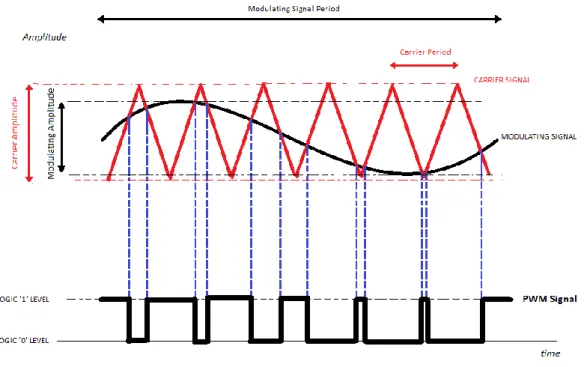
The “Pulse Width Modulation” is a devoted drive technique for “Class-D” amplifiers and bridge type DC-DC converters. The essence of the method relies on modulating a signal by coding its amplitude variations in time (phase angles) into pulse widths of the produced PWM signal as a pulse train [1]. This resulting signal is called “modulated signal” [1]. Obviously, the signal of which amplitude levels are used is called “modulating signal” [1]. The modulation procedure also needs another signal called “carrier signal” in addition to a modulating signal. This is mostly triangular or saw-tooth shaped and compared with the modulating signal with respect to the amplitude [1]. The resulting modulated signal pulse widths are determined by the duration where the modulating signal is bigger than the carrier in amplitude [1]. This scenario is illustrated in “Figure 2” below.
Figure 2 - Pulse Width Modulation Procedure 1.3.2.1 DC-DC Converter
In this type of use of a full-bridge, desired DC voltage levels at the output of the circuitry are produced from an independent level of a supply voltage [1]. In other words, a DC level is converted to another DC level. The modulating signal used here to produce the PWM signals is just a DC level. It is adjusted according to the carrier signal amplitude to get desired levels at the output. The fundamental component level of the voltage across the output load will then be the supply voltage multiplied with the ratio of the modulating DC signal level to the carrier peak [1].
There are two main switching schemes which are called PWM with a bipolar and PWM with a uni-polar voltage switching. For the bipolar case; “switch 1 (TA+)” with “switch 4 (TB-)” and “switch 3 (TB+)” with “switch 2 (TA-)” in “Figure 1” forms two switch pairs. Each switch of the couples, conducts or not simultaneously with their pairs [1]. In addition, the couples also work complementarily among themselves, not
at the same arm operate complementarily. However, for the unipolar switching, only the switches at same arms operate in that fashion. There is no relation in the working of the switches which belong to the different pairs [1].
1.3.2.1.1 PWM with Bipolar Voltage Switching
At the bipolar switching, either one of the pre-defined switch pairs conducts at switching periods (Following calculations are made by no dead time, which is going to be mentioned afterwards, is assumed to be involved.) [1].
As can be seen in “Figure 3” above:
It is found that the conducting duration “ton”of the “switch pair 1” is:
then the duty cycle of the same pair will be:
(
) [1]
The duty cycle of the other pair, pair 2 , which works complementarily with first one is then:
and, the average voltage across the output terminals will be:
[1] Substituting “D1”:
[1] and “
” implies that the average output voltage changes linearly with the input control signal, as it is the case for a linear amplifier [1].
1.3.2.1.2 PWM with Unipolar Voltage Switching
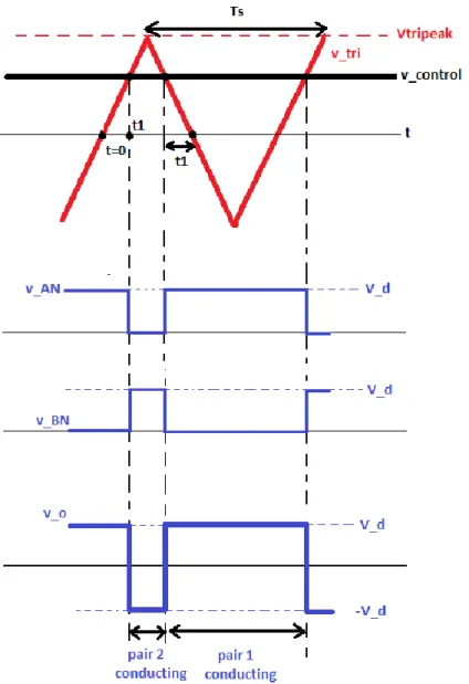
Figure 4 - DC-DC Conversion by Unipolar Switching
In “Figure 4” above, a triangular carrier signal is compared with both the control voltage (modulating signal) “vcontrol” and “-vcontrol” for producing PWM drive signals for the switches resides at first and second arm of the bridge, respectively [1]. States of these switches are determined then as the following comparison suggest:
– [1]
By analyzing the “Figure 4”, it is intuited that the duty cycle values are very similar to the ones bipolar PWM has:
( ) [1]
Thus, the results shows that the average output voltage “Vo” of the unipolar switching PWM is same with the bipolar voltage-switching scheme’s and again it varies linearly with the input control (modulating) signal, “vcontrol” [1].
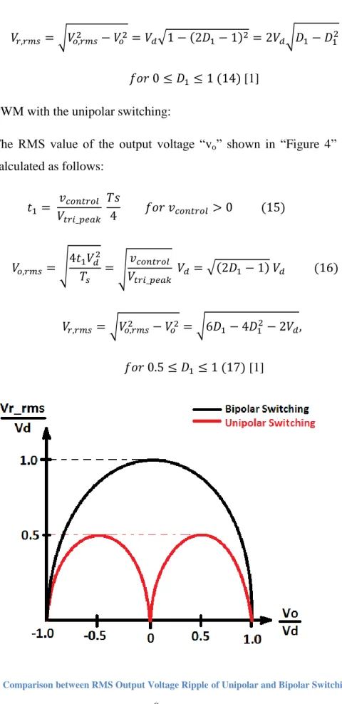
For the same switching frequencies (carrier signal frequency), the use of the unipolar voltage switching method will result in a better frequency response at the output, a spectrum with lowered levels of unwanted harmonics [1]. In other words, ripple magnitudes at output waveforms will be reduced [1]. This is because of the “effective” switching frequency of the output voltage signal is twice the one belongs to bipolar case [1].
The output voltage of the two methods is assumed to be independent of the output load current “io”, because a “dead-time”, which will explained at the following sections, is not involved in PWM drive signals of switches [1]. Then the RMS value of the voltage ripple “Vr” across output terminals in terms of the average “Vo” can be calculated for [1]:
a) PWM with the bipolar switching:
The RMS value of the output voltage signal “vo” shown in “Figure 3” is calculated as follows:
√ √ √ [1]
b) PWM with the unipolar switching:
The RMS value of the output voltage “vo” shown in “Figure 4” can be calculated as follows: √ √ √ √ √ [1]
1.3.2.2 DC-AC Inverter (Class-D Amplifier)
As its name suggests DC-AC inverters are used to produce AC signals from DC levels. This can be done by the use of proper AC modulating (control) signals to produce PWM signals. So, pulse widths vary for different switching periods with respect to the magnitude levels of the control signal sampled at the corresponding switching interval. Desired AC waveforms can be acquired by driving a full-bridge with this PWM signals. Before providing a more detailed explanation of full-bridge DC-AC inverters, a few points should be considered. The ratio of the amplitude of the modulating (control) signal to carrier’s is called the “modulation index”:
This index differs from ‘0’ to ‘1’ in general but also may exceed ‘1’ in some special cases which are called the “over modulation” [1]. The other important ratio is made up from frequencies and it is the ratio of the modulating signal frequency to the carrier’s and called the “frequency ratio” of the pulse width modulation:
[1].
This is another important indicator of modulated signal characteristics accompanied with the modulation index. These characteristic, like the spectrum content, will be explained in further chapters.
The pulse-width modulation techniques which are used to generate drive signals for DC-AC inverters differ from analog to digital systems. Methods used in analog applications can be adapted to digital platforms. This means that the following remarks which have been given for analog systems are also valid for digital ones as well. However, solely digital methods have peculiar features and approaches. 1.3.2.2.1 Analog Technique
comparator which output PWM signals. Although this seems easy in implementation, it is also very sensitive towards small amplitude variations of the input signal because switching instants are determined by detecting exact intersections of continuous signal amplitudes [2]. In theory, this results in a frequency spectrum of output PWM signals with lower levels of harmonics, but the method itself is very error prone under the practical situation of noisy signals. It is not surprising to encounter glitches and spikes in the output waveforms.
1.3.2.2.1.1 PWM with bipolar switching for Full-Bridge
“Figure 6” above shows the procedure of generating bipolar PWM signals for the DC-AC inversion purpose. The only difference from the DC-DC bipolar case is the control signal. Here, it is an AC signal which is a “sinusoid” in this. The third part of the same figure shows a section of the spectrum of the output voltage and it is obvious that the amplitude of the fundamental-frequency component “(Vo)1_peak” is equal to “ma” times “Vd” [1]. This can be analyzed for the sinusoidal PWM by first assuming that “vcontrol” is constant during a switching period where “mf” is provided to be very large [1]. Then the situation here is very similar to the one as in the DC-DC converter bipolar switching scheme, where the average output voltage (the output voltage averaged over switching period Ts) “Vo” depends on the ratio of the “vcontrol” to the “Vtri”for a given “Vd”:
It can also be assumed (though not necessarily) that the “vcontrol”signal changes very little during a switching period, which necessitates “mf”to be large [1]. So, with the assumption made over the “vcontrol”, the above equation indicates the variation of “the instantaneous average value” of the “vo” from one switching instant to the following [1]. This “instantaneous average” is the fundamental component of the “vo” [1]. If the “vcontrol” term at the above equation is substituted with the modulating signal peak value “Vcontrol_peak”, the result will be the peak of the fundamental component of the “vo”, (Vo)1:
[1].
This implies that in a sinusoidal PWM, the fundamental component of the output voltage changes linearly with the “ma” (for ma≤1) in other words with the input control signal level (modulating signal) as in linear amplifiers [1].The range of “0≤ma≤1” is called the linear region [1].
At the output voltage spectrum, harmonics appear at the switching frequency, its multiples and also at their sidebands [1]. This generalization is valid for “ma” values in between 0 and 1 [1]. Theoretically, the harmonic frequencies can be calculated as:
( )
which can be turned into the harmonic order by dividing to the fundamental frequency [1]. Then, it corresponds to the “kth” sideband of the harmonic which is centered at “j” times the frequency modulation ratio “mf”:
( )
where “ ” means the fundamental component [1]. When the “j” is odd, the “k” may only takes even values; for even “j”s, the harmonics occurs only when the “k” is odd [1]. The reason for this will be explained later.
The equation, which is used to calculate the levels of the harmonic components at the output for sinusoidal PWM, is the following output voltage waveform equation (24):
∑ ∑ ( ) ( )
where the is the angular frequency of the control signal and the is the angular frequency of the carrier signal [3].
In “Table 1”, the normalized harmonic levels “( ) ” are given with respect to the amplitude modulation ratio “ma” under the constraint of “mf≥9” [1]. Harmonics up to “j=4” at the “equation (23)” with amplitude levels comparable to the fundamental component are given by using equation (24) [1].
ma 0.2 0.4 0.6 0.8 1.0 h 1-Fundamental 0.2 0.4 0.6 0.8 1.0 mf 1.242 1.15 1.006 0.818 0.601 mf±2 0.016 0.061 0.131 0.22 0.318 mf±4 0.018 2mf±1 0.19 0.326 0.37 0.314 0.181 2mf±3 0.024 0.071 0.139 0.212 2mf±5 0.013 0.033 3mf 0.335 0.123 0.083 0.171 0.113 3mf±2 0.044 0.139 0.203 0.176 0.062 3mf±4 0.012 0.047 0.104 0.157 3mf±6 0.016 0.044 4mf±1 0.163 0.157 0.008 0.105 0.068 4mf±3 0.012 0.07 0.132 0.115 0.009 4mf±5 0.034 0.084 0.119 4mf±7 0.017 0.05
Table 1 - Normalized Harmonic Levels
The “mf” value should be chosen to be as an odd integer for the bipolar PWM to have an odd symmetry “ ” as well as a half-wave symmetry “[ ( )]” as it is the case at “Figure 6” plotted for the “mf = 15” [1]. Therefore, no even harmonics occur at the spectrum of the output voltage signal “vo“ but only the odd ones do [1]. Thus, the “j” and the “k” values can be either odd or even oppositely for an odd “mf” when only non-zero harmonic levels occur at odd harmonic orders.
For selecting the switching frequency, the relative ease in the filtering high frequency harmonics should be considered [1]. For this purpose, it is preferable to determine a high switching frequency as much as possible, with keeping in mind an important resulting drawback: switching losses which is the only significant dissipation source of the inverter which increase proportionally with the switching frequency “fs” [1].
Therefore, in most applications, the switching frequency is chosen to be 20kHz, above the audible range [1].
The discussion of the switching frequency selection is carried on by analyzing situations under specific frequency ratio, “mf”, values. Arbitrarily; frequency ratios under the “21” are specified as small and above this level they are said to be large [1]. For the following evaluations, the amplitude modulation ratio “ma” is assumed to be in the linear region, in between “0” and “1” [1].
Small mf (mf≤21):
1.Synchronous PWM: For the low values of the “mf”, the frequency of the carrier signal should be an integer multiple of the modulating signal’s and the resulting PWM technique will be qualified as the synchronous PWM as shown in “Figure 6” [1]. The reason for the using synchronous PWM rather than the asynchronous (where the “mf” is not an integer) is for avoiding from sub-harmonics which appears close to the fundamental component and should be avoided in most applications [1](book p. 208).
2. Not to have the even orders of harmonics at the output waveforms as discussed previously, the “mf” should be an odd integer for single-phase inverter applications with the bipolar switching PWM [1].
Large mf (mf>21):
The sub-harmonic levels which are observed using the asynchronous PWM as the switching scheme are small at large values of the non-integer “mf“ [1]. Therefore, it is not inconvenient to use the asynchronous PWM with the large values of the “mf”; as it is the case for constant carrier frequency applications where the modulating frequency varies [1].
Over-modulation (ma≥1.0): For linear region values of “ma≤1.0”, harmonics
are shifted towards the switching frequency and its multiples with the drawback of the having fundamental component amplitude at the output
voltage not as great as desired [1]. As explained before, its amplitude varies linearly with the modulation index “ma”. Therefore, to increase the amplitude of the fundamental at the output further, the “ma“ can be increased beyond its linear range to be bigger than “1.0” [1]. The situation is described as the “over-modulation” [1]. However, this results in many more harmonics, even ones at the fundamental frequency multiples, to occur in the output voltage spectrum with respect to the case with “ma≤1.0” [1].
Moreover, not only the fundamental component amplitude quits changing linearly with the modulation index as in the linear range but also it starts to be affected from the frequency ratio “mf“ additionally [1]. This is shown in “Figure 7” below:
Figure 7 - Spectrum Performance of Over-modulation
As it can be seen in “Figure 8” below, increasing the “ma” after a certain value outside the over-modulation range does not increase the fundamental amplitude any more. Since drive signals deteriorate from a PWM waveform and turns into a square wave with the frequency of the modulating signal [1].
As a result, the normalized fundamental component amplitude saturates to “ ” for the “mf=15” [1].
1.3.2.2.1.2 PWM with unipolar switching (double phase)
Figure 9 - DC-AC Uni-polar PWM Switching
As mentioned before, the unipolar PWM switching scheme suggests only the switches at the same arm of the full-bridge work complementarily. In this case, PWM signals are created from a modulating signal and its 180o phase shifted version for controlling the legs A and B separately [1]. The switching instants which are shown
vcontrol > vtri: TA+ on and VAN =Vd vcontrol < vtri: TA- on and VAN =0 (-vcontrol )>vtri: TB+ on and VBN =Vd (-vcontrol )< vtri: TB- on and VBN =0 [1]
For this switching scheme there are not any switch couples acts in the same way as in the bipolar case. Then, there occur four combinations of switch states rather than two. Except the simultaneous conduction and the non-conduction states for the switches at the same arm, every other state is valid as below:
TA+ TB- on: vAN = Vd, vBN=0; vo=Vd TA- TB+ on: vAN = 0, vBN= Vd; vo=-Vd
TA+ TB+ on: vAN = Vd, vBN= Vd; vo=0 TA- TB- on: vAN = 0, vBN=0; vo=0
[1].
The output voltage can has three voltage levels as given above and the only transitions are either between the zero and the “+Vd” or between the zero and the “–Vd” voltage levels [1]. This is why this type of PWM technique is called the unipolar voltage switching [1]. The crucial superiority of this scheme over the bipolar switching is its “effectively” doubling the switching frequency in the output waveforms [1]. Thus, the switching harmonics in the corresponding signal spectrums only occur at the even multiples of the switching frequency and their sidebands. [1].
If the frequency modulation ratio “mf” is selected as an even integer (odd for the PWM with bipolar switching), the harmonics at the exact switching frequency multiples are further disappeared in a single-phase inverter [1]. The fundamental components of the output terminal voltages, the “vAN” and the “VBN” are displaced by 180o from each other’s [1]. Therefore, the harmonic components of these signals
at the switching frequency are in-phase ((ΦAN- ΦBN =180o) * mf =0o, because the “mf” is chosen even) [1]. As a result, the odd number order harmonics of the switching frequency will not appear in the output voltage, “vo= vAN - vBN”, spectrum [1].
For the unipolar voltage switching, the harmonic order “h” is: ( )
the order of the harmonics which occur at the multiples of the “2mf” and its sidebands [1]. Additionally, because the “h” is odd, the “k” can only have odd values for the harmonic order to be odd [1].
If a comparison between the unipolar and the bipolar voltage switching should be made; then it can be said that, in both of the methods, the voltage levels of the fundamental-frequency component of the produced PWM signals are same for the use of equal “ma” values [1]. However, in the unipolar voltage switching with proper selection of the “mf”, no harmonic components occur at odd multiples of “mf” and their sidebands and results in a remarkable reduction in the harmonic content [1]. 1.3.2.2.2 Digital Techniques
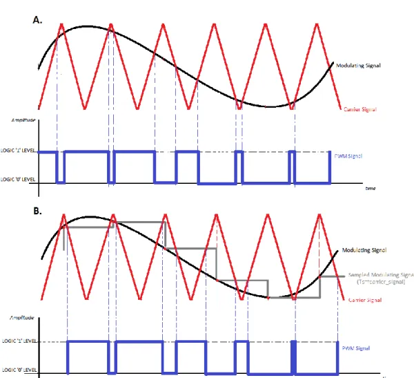
For digital systems, as well as the natural sampling is an option with proper precautions taken, the most basic digital method of the PWM generation is the “uniform sampling”. A similar trouble arises in the digital case of the “natural sampling” as in the analog one and it is caused by the unwanted amplitude variations at the modulating and carrier signals. This time the discrete structure of the signals makes it hard to compare them directly when they are sampled at different rates. As a result, glitches may occur at produced PWM signals. For avoiding this, one solution is to sample the modulating signal with the carrier signal frequency and make the comparison afterwards [4]. This corresponds to the sampling method of the “uniform sampling” [4]. However, this causes to miss the exact intersections of two signals. Therefore, erroneous pulse widths as well as increments in harmonics levels will
these two methods can be seen in “Figure 10” below. If the PWM signals are inspected carefully, it is seen that their widths do differ.
1.3.2.2.2.1 Asymmetrical and Symmetrical Uniform Sampling
Figure 11 - Uniform Sampling Types
In “Figure 11” above, uniform sampling types are illustrated. These are separated into two as the “single sided” (c.) and the “double sided” (a., b.) with respect to the carrier signal shape. For the single sided uniform sampling, the modulating signal is compared with a saw-tooth type carrier signal [4]. This causes only the one of the two switching edges in each switching periods to be determined with the comparison process [4]. The other is just at the instant when the corresponding switching period ends [4]. The shape of the carrier waveform is triangular in the case of the double sided type which requires two comparison operations for deciding the switching instants [4]. This method has the two different implementations of using either one or two samples for determining the switching edges at a switching period [4]. The method is called the “asynchronous uniform sampling” in the case of the use of two samples. This implies the modulating signal should be sampled with the rate of twice the carrier (switching) frequency. The synchronous implementation involves the use of one sample and the modulating signal which is sampled at the switching rate. The output voltage waveform of the asymmetrical uniform sampling of a sinusoid is as the following equation suggests:
∑ ( ) ( ) ( ) … ∑ ∑ ( ( )) ( ) ( ) ( ) [3].
The PWM signal generation is easy and practical with digital platforms. Therefore, there are many different digital modulation techniques with different features [5]. One is the optimizing PWM signals of which switching angles are pre-determined with minimization algorithms for lowering harmonic levels in the output waveforms [5]. The “enhanced uniform PWM”, which will be analyzed following, is the one of these examples among many digital PWM application methods.
1.3.2.2.2.2 Enhanced Uniform PWM – Interpolation (An Alternative Digital Sampling Process)
For producing PWM signals digitally, one proposed solution which emulates the natural sampling is called the “Linear Interpolated Natural Sampling” [3]. This method interpolates the levels of the two consecutive samples of the modulating signal. So, the switching instants are determined more precisely as it is illustrated in “Figure 12” above [3].
The switching time instants which are shown in the figure above the “ ” and the “ ” can be calculated by using the amplitude values of the samples :
where the “T” is the sampling interval which is equal to the half of the carrier signal period [3].
This type of modification improves the uniform PWM by lowering the harmonics levels in the output voltage spectrum [3]. However, their magnitudes do not decay rapidly with the increasing carrier frequency [3] .
For improving this method even more, a weight coefficient of the “ ” in the interval from “0” to “1” can be introduced to modify switching instants [3]. It changes the effect of the sample which determines the following switching instant in a switching period [3]. The pulse edge instants are now calculated as follows:
Figure 13 - Enhanced Uniform Sampling
The function of the weight “ is illustrated in “Figure 13” above. It is deduced that when the “ ”, the method turns out to be the linear interpolated natural sampling [3]. Moreover, setting the “ ” equals to “1” will result with the uniform sampling [3]. The analysis of the spectrum of the enhanced sampling method shows the magnitude of the third harmonic distortion is a function of the coefficient “ ” [3].The minimum distortion caused by this third harmonic is observed for the “ ” to be around “0.35” and this value does not depend on the signal or carrier frequencies [3]. With the use of this new method, it results in that, up to a 30dB decrease can be reached at the third harmonic level with respect to the conventional uniform sampling [3].
1.3.2.3 Dead-Time for Single Phase Inverters
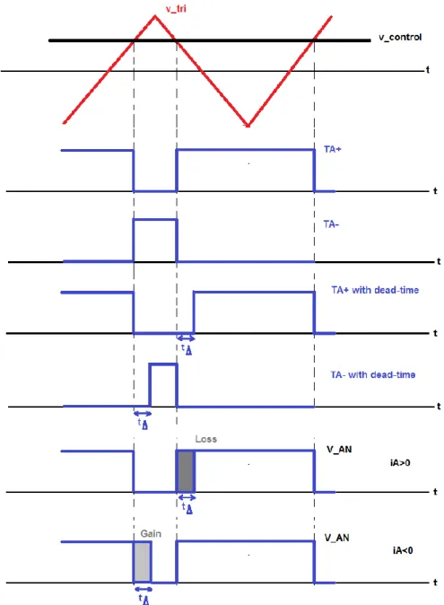
In practice, since the switches used at the bridge have finite turn-off and turn-on times, the switching timings will be updated [1]. The instants of transistors’ going into the conduction state will be delayed for a significant duration of time as can be seen in “Figure 14” [1]. This time durations which are called “dead-time”, “tΔ”,
should be chosen conservatively to prevent the phenomena called “shoot through” [1]. This refers to the cross-conduction when DC supply is shorted through the arms of the bridge [1]. The amount of the dead-time is advised to be chosen a few microseconds for the fast responding MOSFETs [1].
During the dead-time, the switches of the same arm are in non-conducting state, and the output terminal voltage levels “vAN“ or “vBN“ are determined according to the direction of the output load current “iA” as shown in the figure above [1]. For the single phase inverters, the voltage level of the output terminal “A” becomes “Vd” when the “iA<0” and “0” for the “iA<0” because of the path which is provided by the conducting fly-back diodes for the load current. If the ideal voltage waveform of the output terminal “A”, the “vAN“, in which no dead-time is imposed is subtracted from the actual waveform with the dead time, it results in an output voltage error function:
[1].
The variations (defined as a drop if positive) at the output voltage level because of “tΔ” and the average voltage error over a switching period can be calculated as follows:
{
[1].
The “ ” only depends on the direction of the output current but not on its magnitude as can be seen in the equation above [1]. Moreover, it is deduced from the same equation that the “ ” is proportional to the dead-time duration “ ” and the switching frequency “ ” [1]. This is interpreted as the necessity of using fast responding devices which can operate with small dead-time durations in bridge inverter applications which require fast switching (high “ ”) [1].
The same analysis of the output voltage level variations can be made for the output terminal “B” as well, with considering “ ”:
{
Because ” and “ ”, the instantaneous average value of the output error voltage over one switching period “ ” is:
{ [1].
For the application of a full-bridge with the single phase sinusoidal PWM, the instantaneous average output voltage “ ” is given in the “Figure 15” above. The dead-time causes an average voltage distortion in the output when the output current change its direction [1]. This can be modeled as seen in the same figure above and will results in low order fundamental frequency harmonics to appear: like third, fifth, seventh, and so forth [1].
1.3.2.3.1 The Analysis of Dead-Time Effect in PWM Inverter
It is discussed following that the effect of the dead-time on the output voltage spectrum of a full-bridge inverter in detail. A decrement at the fundamental component level as well as an increase in the low-order harmonics levels is observed [6]. It is also shown that these effects of the dead-time duration are highly related with the load power factor [6].
As mentioned before, the output voltage during the dead-time is determined by the output load current direction and it opposes the current flow in either direction [6]. In other words, there occurs such a voltage alteration which makes the current magnitude to be smaller than it should [6].
The following assumptions are made for the analysis:
1-The switching frequency is sufficiently large in comparison with the fundamental frequency,
2-The output current is nearly sinusoidal [6].
These assumptions make possible to calculate the cumulative effect of the dead –time durations, “Td”, by averaging the voltage variations, which occur in these time intervals, over the fundamental period of the output current [6].
At the each switching period, the variation at the output voltage “ ” is calculated by
and its average, “ , over a half cycle of the inverter output current is:
where the “M” is the number of switching per one fundamental cycle and “T” is the fundamental component period [6].
Figure 16 - Dead Time Effect On Fundamental Output Voltage
In “Figure 16” above, the “ ” is the output voltage fundamental component of the inverter in the case of no dead-time effect is ever involved. Additionally, it is assumed that the load is inductive and the current lags the “ ” with the “Φ' ” [6]. The average voltage deviation over an entire fundamental cycle can be treated as the square wave “ ” shown in the figure above [6]. It is shifted 180o
in phase with respect to the output current [6]. The “ ” is the fundamental component of that representative voltage deviation square wave and its RMS value “ ” is calculated as:
In the pre-determined assumption, it is said that the output current is nearly sinusoidal. So its harmonic components are neglected; and the phase difference “Φ” among the and the “I” is defined as the load fundamental power factor [6].
Figure 17 - Phasor Representation of Dead Time Effect
In “Figure 17” above, a phasor diagram is provided which shows that the “ ” and the output current has a 180o phase difference between each other’s [6]. The fundamental component of the output voltage with the dead-time imposed on, “ ”, leads the current with a phase angle of “Φ” [6]. Therefore, a phase difference of “ ” appears between the “ ” and the “ ” [6]. Using the trigonometrical identity for the triangles which has sides of the “ ” and the “ ”, an equation for finding the unknown variable “ ” can be derived:
where the “ ”, the “ ” and the “ ” are the RMS values of the “ ”, the “ ” and the “ ” [6]. Then the solution for the “ ” is:
√ [6].
√
where the “
” is the normalized voltage deviation which is observed at the fundamental component of the output voltage waveform and is in the range of “0< <1” [6].
The RMS value of the “ ” is:
√
where “ ” is the modulation index [6]. Then the normalized voltage deviation can be written in terms of the “M”, the “Td” and the “ ” as:
As pointed before, the power factor does affect the output fundamental voltage level. It can be seen in “Figure 18” above that as the power factor increases, the voltage deviation becomes smaller and the decrement in fundamental current component will be less [6]. The “ √ ” is the ideal value of the output voltage when modulation index is unity [6].
1.3.2.3.2 Harmonic distortion of Dead-Time Effect in PWM inverter output waveforms
Figure 19 - Dead-time Insertion Method
The dead-time durations are inserted into the drive signals in such a way that; the “turn-off” instants are advanced and the “turn-on” instants are delayed for the half of the dead-time duration from the ideal instants [7]. This result in the total dead-time period of the as can be seen in the first part of the “Figure 19” above[7]. In the second part of the same figure the conventional way of the dead-time insertion is illustrated. The method depends on delaying only the turn-on switching edges for the exact amount of the dead-time [7]. Therefore the switching edges will be shifted right in each switching period with respect to the first method proposes [7]. The amount of this duration is the half of the dead-time [7]. As a result the harmonic levels at the switching frequency multiples and at its sidebands will be differ because of the ruining the pulse symmetries in such a way [7]. However, the
low-order harmonics of the fundamental frequency which are considered important mainly will be substantially unchanged [7].
1.3.2.3.2.1 Method of analysis
The analysis of the spectrum is made for the output waveform which is produced with the asymmetrical double-edge uniform sampling pulse-width-modulation is the PWM [7]. This waveform consists of “p” pulses with the characteristics shown in the “Figure 20” below [7]. Then the amplitude of the harmonic which is originated by the pulse can be calculated as follows:
{ } where the “ ” is the supply voltage, the is the switching period, the is the position within the fundamental period of the midpoint of the “kth” pulse [7]. The and the are the normalized half-widths of the pulse; the and the are the ideal half-widths of the same pulse and can be calculated by:
[7].
The harmonic amplitude level is calculated by considering the contributions of all “p” pulses in the fundamental period:
∑ [7].
The dead-time changes the values of the and the into the and the with the employment of the method of the dead-time insertion as proposed in the first part of the “Figure 19” as:
For the positive load current direction: o o For the negative load current direction:
o o [7]
For both of the current directions, these half cycles can be found by calculating “ ” as stated in the section “1.2.3.2-The Analysis of Dead-Time Effect in PWM Inverter ” [7].
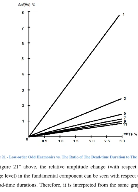
“Figure 21” and “Figure 22” below show that the levels of the low-order harmonics at the output voltage waveforms increase linearly with dead time duration [7]. For example, the calculated 5th harmonic level increases from 1.1% to 5.5% while the dead time duration increases from 5 to 25 us for the corresponding switching period [7].
Figure 21 - Low-order Odd Harmonics vs. The Ratio of The Dead-time Duration to The Switching Period In “Figure 21” above, the relative amplitude change (with respect to the supply voltage level) in the fundamental component can be seen with respect to the amounts of dead-time durations. Therefore, it is interpreted from the same graph that the net amplitude level of the fundamental component at the output voltage waveform decreases linearly while the increasing dead time durations [7].
“Figure 21” also shows that the low-order odd harmonic amplitudes vary linearly with the ratio of the dead-time duration to the switching period “td/Ts” [7]. Therefore, this implies that harmonic levels will not change for the cases of the “td” and the “Ts” values change as long as their ratio stays the same [7]. Then the odd low-order harmonic content of the cases of 10us dead time with a switching frequency of 2 kHz and a dead time of 1us with a switching frequency of 20 kHz will
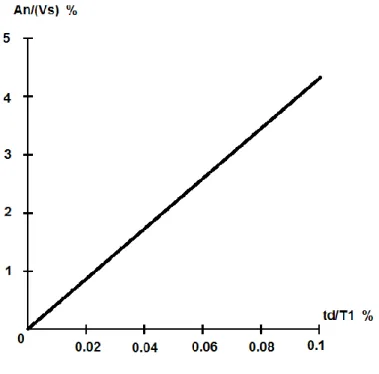
Figure 22 - Low-order Even Harmonics vs. The Ratio of the Dead-time Duration to Fundamental Period for Even Frequency Ratios
The amplitude levels of the even order fundamental frequency harmonics in the output voltage varies with the ratio of the dead-time duration to the fundamental period “td/T1” [7]. It can also be deduced that these levels of the even harmonics do not depend on the switching frequency directly [7].
Chapter 2
Design of the System
2.1 System Layout
The overall system layout is like the one in “Figure 23” below. As for the hardware, an H-bridge has been designed for the driver circuitry. However, before the design was finalized, some alternative designs were tried for this power stage. A detailed analysis is provided in “Appendix A” and the reasons are given in very same section why the alternative design was not successful.
Figure 23 - System Layout
As previously mentioned, a BASYS2 FPGA demo board is used for producing PWM signals. The signals “PWM_A” and “PWM_B” are the complementary PWM signals. The “PWM_A” is the reference for determining the “duty cycle” value. These signals
inverter IC supplied with 5V. This is necessary for the MOS gate driver ICs’ to be able to input signals. Driver ICs are also required to increase PWM signals to full-bridge network supply voltages. For high side transistors to be able to conduct, their gate voltages should be higher than their source voltages which should be either ground reference or circuit supply level. The “PWM_OUT_A” and the “PWM_OUT_B” are the final output voltages of the full-bridge class-D amplifier outputs’. They should be either ground reference or 45V amplifier supply voltage.
2.2 Driver Circuitry – Full Bridge (H-Bridge)
Class-D type amplifiers are very flexible for different operations; by varying drive signals, hardware becomes either a DC-DC converter or a DC-AC inverter [5]. Because these drive signals are mostly produced by microprocessors or controllers; therefore, the operation of the circuitry is a matter of changing of a few lines of the software without altering the hardware [5].
The design of the processor circuitries and codes are extra tasks which the alternative design requires none of it. However, it can be interpreted as a pay for overcoming the troubles which the alternative circuit structure has. This alternative circuit structure is widely used and its responses are known from the many studies that have been done on this. Additionally, the structure itself is simple and not as big as the first option’s Class-A stage. Power transistors are driven as switches by either turning on or off at their SAT regions, as a result only significant power will be dissipated at the switching instants [8]. Therefore, this provides high power efficiency greater than 90% for a large output swing in case of a high modulation index [9]. The reason behind this is the small “SAT” region drain-to-source resistance with respect to the power transistor’s “RDS” of the first option which is used in the active region. This saves designers from using bulky coolers and concern about thermal stability. Although it seems efficient, an extra electrical energy loss occurs from transistors switching as mentioned. However, this will not negatively impact high efficiency; losses are much less than the previous case.
The digital class-D type amplifiers have also astonishingly linear responses and are very immune against noise. Moreover, the circuitry has a wide operation band, as from DC in DC-DC conversion applications and up-to one half of the sampling frequency when it is used as a DC-AC inverter [8]. While providing these advantages, the amplifier can be constructed to be compact which is a crucial feature for mobile systems as here [4].
Among other digital D-type amplifier structures like the half-bridge, the full-bridge is selected in this work despite space concerns because of the additional number of its components. Because the maximum output voltage swing that can be provided by a full-bridge inverter is twice that of the half-bridge under the same supply voltage levels, the full-bridge is selected [1]. This means that more output current levels and as well as higher electromagnetic fields can be reached. Also with the use of the full-bridge there is no need for dual polarity power supplying as in the half-full-bridge in order to have DC free output waveforms.
In addition, for the microprocessor side, a Xilinx FPGA is used to produce PWM signals digitally. The choice is favorable because FPGA promises concurrent operation, less hardware (demo boards), comparatively low cost for a complex circuitry and quick prototyping [10].
2.2.1 Circuit Simulations
Simulated analogue circuitry is as seen in “Figure 24 - Simulation Circuit” below. The “U1” and the “U2” are MOS gate drivers. The typical application circuitry provided in the datasheet of this product is set up with other passive components. Power MOSFETs are named as the “Q1, Q2, Q3 and Q4” and the load inductor is modeled with “L1”. Digital PWM signal inputs of the gate drivers are pulse trains with 20 kHz frequency and constant duty cycle of 95% (5% complementary signal). They are also produced with a fundamental frequency of 600 Hz by using analog comparator and 20 kHz carrier with a 600Hz sinusoidal signal.
Figure 24 - Simulation Circuit
The full bridge is constructed from two arms of transistor couples. “Q1 and “Q2” couples reside at the 1st arm and the “Q3 and Q4” couple at the 2nd. Also term high side transistors or switches are used for pointing the “Q1 and Q3” couple while low side mean “Q2 and Q4”. As will be explained in the section employed PWM techniques, for both AC and DC cases (PWM with variable or constant duty cycle) only one transistor conducts at each arm and side. This type of drive is called “Bipolar PWM”.
The load inductor at the output of the bridge circuit filters the PWM voltage signal and provides electrical current with a fundamental frequency of same PWM signal. Its low pass filtering characteristic can be modeled by considering a 126mH inductance and a 22.6 Ω serial resistance as seen in “Figure 25” below. In practice, the inter-winding capacitance disturbs this response. At much higher frequencies than the range of the graph below, low pass filtering characteristic of the inductor degrades. Thus, current ripples are observed in the output, originated from the switching frequency harmonics in PWM drive signals.
Figure 25 - Load Inductor Frequency Response
As stated before, transistors in the circuitry operate like switches changing between on and off. In other words transistors are used outside their active regions of I-V characteristics. This situation provides efficiency and keeps transistors from dissipating much energy which requires thermal precautions.
As mentioned before, MOS gate drivers are required to make high side transistors able to open. This is because the conducting high side transistor has a source voltage of “Vcc-VDS(SAT)”. Then for these transistors to be able open, their gatevoltage must be higher than the source voltage plus the gate-to-source threshold voltage. Thus to be able pull FPGA PWM output voltage signal levels to such high levels like Vcc, gate drivers are used.
As mentioned before, when PWM drive signals with constant duty cycles (DC [modulation] case) are used, the average voltage across the circuit output is: “ ”. If this value is divided by the serial resistance of the inductor, it will be found that the fundamental DC current flows through the inductor. For the supply voltage “Vcc” of 48V, if 95% duty cycle PWM voltage signal is applied across the load inductor with a 22.6 Ω internal resistance, the load current will be approximately:
like the simulation result in “Figure 26” below.
In this case, the power driven from the DC supply is approximately:
Figure 26 - Load Inductor Current
The PWM drive signals with variable duty cycle are produced in the AC mode. In this simulation, a sinusoid with 600Hz frequency is modulated in 95% modulation index with a 20 kHz carrier and fed into the gate drivers. From “Figure 25”, it can be seen that the load inductor model has a cut-off frequency of 28.3 kHz and attenuation at 600 Hz frequency is "-53.5dB". Therefore the output current flowing through the inductor is similar to the simulation result in “Figure 27” below.
Figure 27 - Load Inductor Current AC Mode
In the graph above, the current ripple can be observed significantly. As mentioned before this is because of the switching frequency harmonics which cannot be attenuated fully.
2.3 Choice of PWM Method
The circuit structure choice is explained in the previous section and now the employed method of the PWM generation will be discussed following.
The frequency spectrum of the PWM drive signals can be analyzed by using the equations (24) and (26) which was given previously for the sinusoidal PWM waveforms generated with the “double-edged natural” and the “asymmetrical uniform sampling” methods respectively [3]. After an evaluation of these expressions, it results in that the harmonic levels and their distribution over the frequency spectrum differ between the two PWM techniques and yet these harmonics can be specified as the two different kinds of distortion components:
1) The forward harmonic components which appear at the odd multiples of
the modulating signal frequency are confined within the first term of the equation (26) [3]. These belong to the uniform sampling and do not exist in the natural sampling [3].