Silicon and III-V compound nanotubes: Structural and electronic properties
E. Durgun, S. Tongay, and S. Ciraci*Department of Physics, Bilkent University, Ankara 06800, Turkey
共Received 22 October 2004; revised manuscript received 27 April 2005; published 12 August 2005兲
Unusual physical properties of single-wall carbon nanotubes have started a search for similar tubular struc-tures of other elements. In this paper, we present a theoretical analysis of single-wall nanotubes of silicon and group-III-V compounds. Starting from precursor graphenelike structures we investigated the stability, energet-ics, and electronic structure of zigzag and armchair tubes using the first-principles pseudopotential plane wave method and finite temperature ab initio molecular dynamics calculations. We showed that 共n,0兲 zigzag and 共n,n兲 armchair nanotubes of silicon having n艌6 are stable but those with n⬍6 can be stabilized by internal or external adsorption of transition metal elements. Some of these tubes have a magnetic ground state leading to spintronic properties. We also examined the stability of nanotubes under radial and axial deformation. Owing to the weakness of radial restoring force, stable Si nanotubes are radially soft. Undeformed zigzag nanotubes are found to be metallic for 6艋n艋11 due to the curvature effect; but a gap starts to open for n 艌12. Furthermore, we identified stable tubular structures formed by the stacking of Si polygons. We found AlP, GaAs, and GaN共8,0兲 single-wall nanotubes stable and semiconducting. Our results are compared with those of single-wall carbon nanotubes.
DOI:10.1103/PhysRevB.72.075420 PACS number共s兲: 73.22.⫺f, 68.43.Bc, 73.20.Hb, 68.43.Fg
I. INTRODUCTION
Carbon nanotubes are unique one-dimensional nanostructures1 with their exceptional mechanical,
elec-tronic, and magnetic properties.2–5While the use of
single-wall carbon nanotubes共SWCNTs兲 requires a completely dif-ferent paradigm in the development of nanodevices, Si still continues to attract interest for electronic applications in nanotechnology. Therefore, Si-based nanotubes have been the subject of experimental and theoretical analysis.
Even if a single-wall Si nanotube 共SWSiNT兲 has never been observed, theoretical predictions have been performed for various kinds of Si tubes. Fagan et al.6,7have investigated
the structural and electronic properties of chiral SWSiNTs based on density functional theory 共DFT兲. Barnard and Russo8have examined the dependence of the heat of
forma-tion and the binding energy of SWSiNTs on their radius and chirality. The stability of共10,0兲 SWSiNT has been examined by using the empirical Monte Carlo molecular dynamics method and found that it is stable at finite temperature.7
Ivanovskaya et al.9 investigated hypothetical Si nanotubes containing regular chains of metallocarbonedrenes using a one-dimensional tight-binding model within the Hückel ap-proximation. By using ab initio calculations, Dumitrica et
al.10 described how the smallest 共2,2兲 and 共3,0兲 SiNTs are
stabilized by the axially placed metal atoms from different groups of the Periodic Table. Ponomarenko et al.11 studied
the energetics and relative stability of infinite and finite, clean, and hydrogenated open-ended Si nanotubes by using the extended Brenner potential. The existence of H-doped stable tube-shaped finite SiNTs have been predicted12 and
their electronic structures have been compared with those of carbon nanotubes.13 Seifert et al.14 have argued that
struc-tures of silicate and SiH nanotubes are more stable than bare Si nanotubes. Singh et al.15have investigated the stability of
finite and infinite hexagonal prismatic structures of Si with 3d magnetic elements and predicted that such structures can
be stabilized through doping by the transition metal 共TM兲 elements. Fullerene-structured Si tubulars, possibly based on Si24 have been produced.16 More recently, the successful
synthesis of multiwalled Si nanotubes has been reported.17
Now, SWSiNTs are no longer hypothetical structures and it is not unrealistic to expect their fabrication with controllable size and diameter. Similarly, achievements of the synthesis of single-wall BN nanotubes18and GaN共Refs. 19 and 20兲 and
AlN 共Ref. 21兲 thick-wall tubular forms has increased the interest in the theoretical analysis of compound nanotubes.22–25In addition, the synthesis of Mo and W
chal-cogenide nanotubes26–28 and also NiCl tubular and cage structures have been realized.29
In this paper we present a theoretical analysis of Si nano-tubes and III-V compound nanonano-tubes based on state-of-the-art first-principles calculations. Our work is concentrated mainly on the tube structures which can be viewed as the rolling of graphenelike honeycomb planes of Si or III-V el-ements on a cylinder of radius R. Starting from the precursor graphenelike honeycomb structures we investigated their sta-bility, energetics, and electronic properties of these nano-tubes. Since O, O2, Si, Au, and H are critical elements for
various processes on Si, we also examined the adsorption of these atoms on SWSiNT. Finally, we studied the stabilization of unstable, small-diameter SWSiNTs through the internal and external adsorption of transition metal elements. In ad-dition, we found that tubular structures which are generated by stacking of triangles, pentagons, and hexagons of Si are stable and metallic. The共8,0兲 zigzag tubes of AlP, GaN, and GaAs are stable and semiconducting. The results obtained from the present study have been compared systematically with those of SWCNT. The stable tube structures predicted in this study are hoped to motivate experimental research aiming at the synthesis of various tubular structures of group-IV elements and III-V and II-VI compounds.
II. METHOD
We have performed first-principles plane wave calculations30,31 within DFT32 using ultrasoft
pseudopotentials.31,33The exchange correlation potential has
been approximated by the generalized gradient approxima-tion共GGA兲.34Structures incorporating TM atoms have been
calculated using spin-polarized GGA. For partial occupan-cies we use the Methfessel-Paxton smearing method.35 The
width of smearing is chosen between 0.01– 0.1 eV, depend-ing on the system. All structures have been treated by super-cell geometry using the periodic boundary conditions. To prevent interactions between adjacent structures, a large spacing共⬃10 Å兲 has been taken. Convergence with respect to the number of plane waves used in expanding Bloch func-tions and k points in sampling the Brillouin zone are tested for the parent bulk crystals as well as tubular structures. In the self-consistent potential and total energy calculations, the Brillouin zone of nanotubes has been sampled by 共1⫻1⫻19兲 mesh points in k space within the Monkhorst-Pack scheme.36Calculations of graphene and graphite
struc-tures have been carried out using 共19⫻19⫻1兲 and 共8⫻8 ⫻6兲 k point samplings, respectively. A plane-wave basis set with kinetic energy cutoff 200 eV艋ប2兩k+G兩2/ 2m艋330 eV
has been used. All atomic positions and lattice parameters are optimized by using the conjugate gradient method where total energy and atomic forces are minimized. The conver-gence for energy is chosen as 10−5eV between two ionic
steps, and the maximum force allowed on each atom is 0.05 eV/ Å.
It should be noted that DFT-based methods provide reli-able predictions, for the ground state properties, but band gaps are usually underestimated. Hence the energy band structure obtained from the single-particle energy eigenval-ues of Kohn-Sham equations are only approximations to the real energy bands. Proper many-body self-energy corrections can be made by using the GW method.37 Recently, GW
en-ergies are compared with DFT local-density-approximation 共LDA兲 results of 共n,0兲 SWCNTs, which indicate shifts of valence and conduction bands and a considerable increase of the LDA band gap from 0.2 eV to 0.6 eV.38 It is suggested
that GW corrections are small for large radius SWCNTs. Per-forming first-principles many-body Green’s function calcula-tions Spataru et al.39 showed that the optical spectrum of both semiconducting and metallic small-radius SWCNTs ex-hibit important excitonic effects due to quasi-one-dimensional nature. It is interesting to note that while the band gaps of共9,0兲, 共12,0兲, and 共15,0兲 zigzag SWCNTs have been measured by scanning tunneling spectroscopy40 to be
80, 42, and 29 meV, respectively, the same band gaps have been predicted by GGA calculations41 to be 93, 78, and
28 meV, respectively.
The stability of the structures we studied is the most cru-cial aspect of our work, since it provides valuable informa-tion for the synthesis of these materials in the future. In this respect an extensive analysis of stability has been carried out for various nanotubes. First, we applied a radial deformation to certain nanotubes and optimized their structures to see whether they relax to their original, undeformed circular
forms under zero external force. Furthermore, we have per-formed, finite-temperature ab initio molecular dynamics cal-culations up to 1000 K using the Nosé thermostat42 for 250
time steps共0.5 ps兲 to check whether the optimized structure will be affected from random thermal motion of atoms or whether they maintain their tubular form at high tempera-tures. We believe that if there were any kind of structural instability, it would be initiated and also enhanced within these time steps at high temperatures.
III. HONEYCOMB STRUCTURE OF SILICON AND III-V COMPOUNDS
One of the main difficulties for synthesizing Si nanotubes seems to be the absence of a two-dimensional 共2D兲 silicon layer similar to the graphene structure of carbon. This is traced to the fact that in contrast to carbon, sp3hybridization in Si is more stable than sp2hybridization.43 In view of this
situation, we examined whether the graphenelike 2D sheet of silicon can be stable. Two-dimensional hexagonal lattice forming a honeycomb structure in the xy plane has been periodically repeated along the z axis with 10 Å spacing to minimize interlayer interactions. In order to reduce the ef-fects of the constraints to be imposed by using the primitive unit cell, we performed structure optimizations on the 共2⫻2兲 cell in the xy plane. Our calculations revealed that the planar structure 共where all atoms lie in the same plane兲 is metastable, but it is buckled by a 0.45 Å relative vertical displacement of alternate atoms on the hexagons. The gain of energy upon buckling is 30 meV/ atom. The binding energy is calculated to be 4.9 eV/ atom which is 0.6 eV lower than the Si diamond structure and the average distance between nearest Si atoms is 2.2 Å. In the rest of the paper, this graphenelike structure will be specified as the buckled hon-eycomb structure. As shown in Fig. 1, the detailed band structure and total density of states共TDOS兲 analysis indicate that both buckled and planar systems have large band gaps along ⌫K and MK directions, but conduction and valence bands cross the Fermi level at the k point of the Brillouin
FIG. 1. 共Color online兲 Band structure and TDOS analysis for planar and HC of Si. Light lines correspond to planar 共having
P6 / MMM symmetry兲 and dark lines correspond to buckled
struc-ture共having P-3M1 symmetry兲. The zero of energy is set to the Fermi level EF. The inset shows the 1 / 12 of hexagonal Brillouin
zone. The electronic structure of the system does not change significantly as a result of buckling, except some of the bands split due to the lowering of the rotation symmetry. Using a similar method but different pseudopotentials and an exchange correlation potential, Takeda and Shiraishi44 have
examined planar and buckled honeycomb structures of Si. Our results, obtained in a four times larger cell, hence allow-ing more variational freedom, are in overall agreement with the results in Ref. 44. Moreover, we performed an ab initio molecular dynamics calculations on a 2⫻2 supercell, pro-viding further evidence that the buckled honeycomb struc-ture is stable at 500 K for 250 time steps.
Next we address whether a graphitelike structure of Si共or graphitic Si兲 can form. Our study distinguished chemisorp-tion and physisorpchemisorp-tion states in the interlayer interacchemisorp-tion, in contrast to only the physisorption state in graphite.45 The
chemisorption state corresponding to a smaller lattice param-eter c = 6 Å is energetically more favorable, namely the bind-ing is 5.1 eV, which is 0.4 eV smaller than that of the bulk Si. We note, however, that lattice parameters and binding energies depend on the approximation of exchange-correlation potential.46,47 Present GGA calculations yield relatively larger interlayer distance and require the incorpo-ration of long-range Van der Waals共VdW兲 interaction. Such an analysis showing that the lattice parameter of graphite calculated by GGA is improved by including the VdW at-traction, has been presented elsewhere.48
Similar to Si, the honeycomb structures of AlP, GaAs, and GaN are found to be stable also, but less energetic relative to the bulk crystal by 0.8, 1.1, and 0.6 eV per basis, respec-tively. However, the buckling is not favored in order to hinder the formation of a dipole layer.
IV. SINGLE-WALL SILICON NANOTUBES A. Energetics and stability
Having discussed the stability of buckled Si honeycomb structure共Si-HC兲, now we present our systematic analysis of 共n,0兲 zigzag and 共n,n兲 armchair SWSiNTs for different n values; namely n = 3 – 14 for zigzag and n = 3 , 6 , 9 for arm-chair structures. The 共3,0兲 zigzag SWSiNT has clustered upon structure relaxation, indicating that it is not stable even at T = 0 K. While the structure optimization has resulted in regular 共4,0兲 and 共5,0兲 tubular structures, the ab initio mo-lecular dynamics共MD兲 calculations showed that these nano-tubes eventually transform into clusters at higher tempera-tures as shown in Fig. 2. Significant distortions can be easily noticed in共6,0兲 and also 共7,0兲 SWSiNTs, but tubular charac-ter and hexagonal structures on the surface have remained. The共6,0兲 zigzag tube, which has a radius of R=3.8 Å as well as those with larger radii remain stable at temperatures up to 800 K. Barnard and Russo8 also reported the instability of
共3,0兲 SWSiNT in their first-principles study, but they consid-ered共4,0兲 and 共5,0兲 SWSiNTs as stable structures, depending on their geometry optimization performed at T = 0 K. Present results set a limit for fabricating small radius SWSiNTs. The first and second nearest-neighbor interactions between Si at-oms become relevant for the stability of small radius nano-tubes and causes clusterings, if R⬍3.8 Å. Similar behavior
is also obtained for共n,n兲 armchair SWSiNTs. For example 共3,3兲 SWSiNT is clustered at 800 K in spite of the fact that geometry optimization yields tubular structure at T = 0 K. On the other hand, the共6,6兲 tube with a relatively larger radius remained stable at 800 K after 250 time steps. In contrast to 共n,n兲 SWSiNTs, which are found unstable for n⬍6, the 共3,3兲 SWCNT is known to be stable and experimentally fabricated.49,50The difference in the chemical behavior of C
and Si can be traced to the difference in their -bonding capabilities. Si tends to utilize all of its three valence p or-bitals, resulting in sp3 hybridization. In contrast, the
rela-tively large promotion energy from C-2s to C-2p orbitals explains how carbon will activate one valence p orbital at a time leading, in turn, to sp, sp2, sp3 hybridizations in one-dimensional 共1D兲, 2D, and three-dimensional 共3D兲 struc-tures. This is the explanation why tubular structures of C are more stable than those of Si.13 Moreover, since the
inter-atomic distance increases significantly in going from C to Si, the - overlap decreases accordingly, resulting in much weaker bonding for Si tubes in comparison with that for carbon tubes.
After the discussion of stability, we next analyze the en-ergetics, namely the behavior of binding energy 共Eb兲 as a FIG. 2. Structures of共4,0兲, 共8,0兲, and 共6,6兲 SWSiNTs at T=0 and T = 500 K after 250 time steps. A tubular structure has remained in共6,6兲 and 共8,0兲 SWSiNT, but the 共4,0兲 structure has clustered.
function of the radius 共or n兲 of the tube. Eb per atom is
calculated using the expression,
Eb=兵ET关SWSiNT兴 − N共ET关Si兴兲其/N 共1兲
in terms of the total energy of the optimized SWSiNT having
N Si atoms per unit cell, ET关SWSiNT兴, and the total energy
of N, free Si atom ET关Si兴. It is found that Eb⬃4.9 eV and
slightly increases as the radius R 共or n兲 increases for both zigzag and armchair SWSiNTs as displayed in Fig. 3. The energy increase with n is small. According to our results Ebs
of共n,n兲 armchair SWSiNTs are ⬃0.05 eV larger than those of共n,0兲 zigzag ones because of their relatively larger radius at a given n. Corresponding Ebfor SWCNTs is calculated to
be 9.1 eV,51 theoretically.
Finally, the strain energy per atom is calculated relative to the energy of the honeycomb structure,
ES= Eb关SWSiNT兴 − 共Eb关Si-HC兴兲, 共2兲
by subtracting the binding energy 共per atom兲 of optimized honeycomb structure, Eb关Si-HC兴 from the binding energy of
SWSiNT. A slight increase in strain energy is observed as the radius R or n decreases. This is an expected result, since the structure becomes more graphenelike with the increasing ra-dius. Calculated strain energies given by the inset in Fig. 3 are also in agreement with the results obtained by Fagan et
al.7 and Barnard and Russo.8 The calculated value of the
strain energy of a zigzag SWSiNT is smaller than the strain energy of a zigzag SWCNT with a comparable radius.41 In
the classical theory of elasticity, the strain共or curvature兲 en-ergy of a tubular structure is given by the expression ES
=␣/ R2, where␣is a function of Young’s modulus and
thick-ness of the tube’s wall.5,52The results of the present
calcula-tions in Fig. 3 gives a fair fit to the expression,␣/ R2 with
␣⬃2.07 eV/Å2.
B. Mechanical properties
Radial flexibility is a criterion for the stability of tubular structure. SWCNTs are known to be flexible for the defor-mations in radial directions:53,54they can sustain severe
ra-dial deformation transforming the circular cross section into an elliptical one with minor 共b兲 and major 共a兲 axes. The radial deformation on a bare tube of radius R is specified in terms of the strain associated with the pressing of the tube along the minor axis,⑀yy=共b−R兲/R and the strain associated
with the expansion of the tube along the perpendicular major axis ⑀xx=共a−R兲/R. Theoretical and experimental research
has shown that radially deformed tubes relax reversibly to the original circular cross section whenever the external ra-dial force is lifted.55 Moreover, radial deformation can modify the electronic structure reversibly, which leads to a tunable band gap engineering.55,56 For example, a
semicon-ducting共n,0兲 can be metallic under radial deformation. Our results indicate that SWSiNTs display a behavior different than that of SWCNTs. We performed a systematic analysis of radial strain for 共8,0兲 zigzag and 共6,6兲 armchair SWSiNTs. First, these tubes have been deformed by applying ⑀yy
= −0.1, −0.2, and −0.3. Then the stress共or constraint兲 impos-ing these radial strains has been lifted and the structure has been optimized. Contrary to the situation in carbon nano-tubes, up to the applied strain⑀yy艋−0.2 the SWSiNTs have
remained in the deformed state. For example, 共8,0兲 tubes with an initial radial strain of⑀yy= −0.1 and −0.2 are relaxed
to a plastic deformation corresponding to ⑀yy= −0.09 and
⑀yy= −0.14, respectively. Similar results have been obtained
for 共6,6兲 armchair SWSiNT with initial radial strain of ⑀yy
= −0.1 and −0.2. In contrast, the tubes, which initially strained by⑀yy= −0.25 and −0.3 have relaxed to a state with
negligible residual strain. The total energy of the undeformed SWSiNT ET
o
have been found to be lower 共more energetic兲 than the total energy ET
r共⑀
yy兲 of tubes which were relaxed
upon radial deformation −0.3艋⑀yy艋0. However, the energy
difference⌬E=ET r共⑀
yy兲−ET
o⬎0 is very small. The weakness
ofbonds of Si as compared to carbon nanotubes is possi-bly a reason why the restoring forces are not strong enough to derive the deformed state to relax back to the original undeformed state. Once the applied radial deformation gets significant 共兩⑀yy兩⬎0.2兲 the restoring forces become strong
enough to derive the relaxation towards circular cross sec-tion. On the other hand, after a severe radial strain that causes a significant coupling between opposite internal sur-faces, the deformed state may be more energetic 关i.e.,
ET r共⑀
yy兲⬍ET
o兴 or it may relax to different structures such as
clusters. This situation constitutes an important difference between Si and C single-wall nanotubes.
The axial strength of SWSiNT, or the elastic stiffness along tube axis, is defined as the second derivative of the strain energy per atom with respect to the axial strain ⑀zz,
namely = d2E
T/ d⑀zz2. The elastic stiffness of the 共8,0兲
SWSiNT along its axis is calculated to be 23 eV. This value is significant, but smaller than that of SWCNT which is cal-culated to be 52– 60 eV.57
C. Electronic structure
A systematic analysis of the electronic structure indicates that metallic zigzag SWSiNTs 6艋n艋11 have three bands
FIG. 3. 共Color online兲 The calculated binding energy per atom for共n,0兲 zigzag and 共n,n兲 armchair SWSiNTs. The dark region indicates that tubular structures are unstable at finite temperature. The calculated strain energies ES per atom for 共n,0兲 and 共n,n兲
crossing the Fermi level, but a band gap between the valence and conduction bands opens when n艌12. A similar effect has been obtained for zigzag SWCNTs when n艌7.5,41This
metal-semiconductor transition was attributed to the energy shift of the singlet * band which is normally empty, but becomes filled due to increased *-* hybridization at a
small radius.41,58 In the present case it appears that *-*
hybridization becomes significant at a relatively larger ra-dius. The conductance of all these infinite, perfect tubes 共6 艋n艋11兲 is predicted to be equal to 3Go 共Go= 2e2/ប兲. A
similar metallic behavior is also obtained for armchair types, namely for 共6,6兲 and 共9,9兲 SWSiNTs. The conductance of ideal infinite共n,n兲 tubes is 2Go, but not 3Go, as in metallic
共n,0兲 zigzag tubes. Figure 4 presents the systematic analysis of共n,0兲 tubes for 7艋n艋14 and clearly shows how the sin-glet* band gradually raises as R increases.
Based on LDA calculations, Fagan et al.6,7 also found
共6,6兲 and 共6,0兲 SWSiNTs metallic, but they predicted 共10,0兲 and共12,0兲 zigzag nanotubes are semiconductors with a small band gap of 0.1 eV. The disagreement between the present one and those of Fagan et al.6,7may be due to the differences in pseudopotentials and in the approximation of exchange correlation potential. Note that the transition of 共n,0兲 SWSiNTs from the metallic to the semiconducting state through the gap opening may occur at n, which is smaller than predicted by the present study as well as by Fagan et
al.,6,7if self-energy corrections are taken into account by the
GW method.37 Electronic structure analysis performed for
the tubes under strain both radially and axially showed that the metallic character is not altered but the position of the Fermi level is slightly changed due to deformation. The modification of the electronic structure with chirality may offer the possibility of fabrication of nanodevices using SWSiNT junctions. On the other hand, SWSiNTs can be used as metallic interconnects, since their conductance is not severely affected by deformation.
D. Interaction of SWSiNT with atoms and molecules
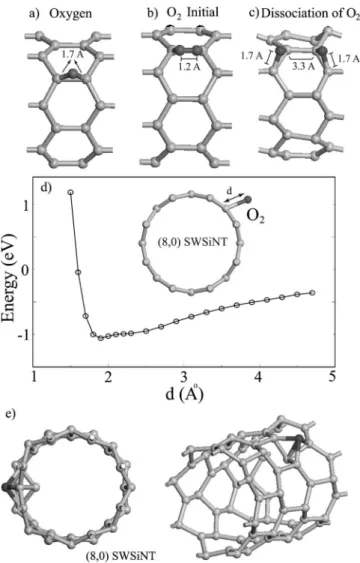
The interaction of Si nanotubes with an oxygen atom and an oxygen molecule is extremely important for technological applications. The adsorption of an oxygen atom is studied by placing it initially above a Si– Si bond parallel to the axis of a共8,0兲 SWSiNT. The optimized structure shown in Fig. 5共a兲 has a very strong chemical bonding between O and SWSiNT with Eb= 8.1 eV and the nearest Si– O distance 1.7 Å. The
resulting geometry showed that SWSiNT is slightly distorted upon O adsorption.
The interaction between O2 and SWSiNT has been re-vealed by calculating the binding energy as a function of the separation d from the axial Si– Si bond of the tube as shown in Fig. 5共b兲. The O2 molecule is kept unrelaxed and taken
parallel to the Si– Si bond. The calculated energy versus dis-tance curve E共d兲 in Fig. 5共d兲 shows that O2can be attracted
to the tube, but there is no physisorption state as in O2 FIG. 4. 共Color online兲 The energy bands calculated for 共7,0兲,
共9,0兲, 共10,0兲, 共11,0兲, 共12,0兲, and 共14,0兲 SWSiNTs using GGA. The lowest conduction band, or singlet*band, is indicated. The zeros
of energy are set at the Fermi level.
FIG. 5.共a兲 The optimized geometry of an O atom adsorbed over the axial site of共8,0兲 SWSiNT. 共b兲 Initial adsorption geometry of O2over the axial site. 共c兲 Dissociation of O2after relaxation and
formation of Si– O – Si bridge bands over the adjacent zigzag Si– Si bonds.共d兲 Variation of interaction energy as a function of the dis-tance d of an O2molecule from the parallel axial Si– Si band.共e兲 Optimized geometry of a single Si atom adsorbed on the top site 共indicated by a dark ball兲.
+ SWCNT.48 The minimum of E共d兲 occurs at 1.9 Å. Upon
relaxation of the tube and O2 near this minimum, the
mol-ecule has been dissociated to form two Si– O – Si bridge bonds over the zigzag Si– Si bonds, and concomitantly SWS-iNT has been distorted locally as illustrated in Fig. 5共c兲. The distances between nearest Si– O and O – O are 1.7 and 3.3 Å, respectively. We repeated the structure relaxation by initially placing O2at a larger distance d = 2.5 Å from the surface of the tube and we obtained the same dissociated state. Our results indicate that there will be a strong interaction between the Si nanotube and the oxygen molecule in open air appli-cations.
The SWSiNT surface is found to be reactive against Si, H, and Au atoms. The Si atom attached to the top site is bound by Eb⬃5 eV. One Si atom of the tube is plunged inside the
tube and a small cluster is formed at the surface 关see Fig. 5共e兲兴. The chemisorption energy of H and Au atoms is strong and found to be 4.4 eV and 3.4 eV, respectively.
V. STABILIZATION OF SILICON NANOTUBES BY TRANSITION METAL ATOM DOPING
Recently, Singh et al.15 showed that Si-cluster structures
and Si-tubular structures formed by top-to-top stacking of Si hexagons can be stabilized by the implementation of TM atoms inside these structures. Those structures are not only stabilized, but also acquired magnetic properties. Earlier, TM atoms are shown to form rather strong bonds with the carbon atoms on the surface of SWCNTs.51 Motivated by the work
of Singh et al.,15we investigated whether共3,0兲 SWSiNT can
be stabilized in the same manner. The共3,0兲 tube has radius
R⬃2.4 Å in which interaction between the atoms located at
the opposite walls of the tube as well as excess strain on the Si– Si bonds are the prime causes of structural instability even at T = 0 K. On the other hand, the radius of 共3,0兲 is comparable to the sum of the ionic radii of V and Si, i.e.,
RV+ RSi= 2.27 Å, and hence V atoms can easily be
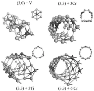
accom-modated inside the tube. We considered a 共3,0兲 SWSiNT, which has V atoms implemented inside and periodically ar-ranged along the tube axis. Because of the supercell geom-etry used in the calculations both linear chains 共LC兲 of V atoms共V-LC兲 and 共3,0兲 tube have a common lattice param-eter共see Fig. 6兲. The optimized structure which that consists of planar hexagons is stacked with V-LC passing through its center, and has been found to be stable. The energy of the V-stabilized structures is lowered by 12.9 eV relative to the energies of the V-LC and the Si tube without V-LC in it but they have the same atomic structures as Si tube with V-LC. Spin-relaxed calculations resulted in zero magnetic moment = 0. The p-d hybridization between Si and V atomic orbit-als is the cause of stability and lowering the total energy.
The radius of the unrelaxed共3,3兲 SWSiNT of 3.7 Å is too large and may not be suitable for its stabilization through the implementation of an atomic chain. Perhaps it may be better suited to accommodate a small clusters of atoms. We consid-ered the possibility whether the共3,3兲 SWSiNT is stabilized by TM atoms adsorbed on the external surface of the tube. To this end, we studied Ti and Cr atoms adsorbed on the hollow sites共i.e., above the hexagons formed by Si atoms兲.
As shown in Fig. 6, we examined three different 共3,3兲 + TM structures: namely, 3 Ti-LC, 3 Cr-LC, and 6 Cr-LC are adsorbed on the 共3,3兲 SWSiNT surface. Spin-relaxed GGA calculations are carried out to optimize the geometric struc-ture. The external absorption 3 Ti-LC关or three Ti atoms per unit cell of 共3,3兲 tube兴 prevented the tube from collapsing into a cluster, but the circular cross section changed to a polygonal one. The ground state has been predicted to be nonmagnetic with= 0. The external adsorption of 3 Cr-LC also resulted in a polygonal cross section, but a ferromag-netic ground state with the net magferromag-netic moment = 9.7B
共Bohr magneton兲. The circular cross section is maintained by the adsorption of 6 Cr-LC. This latter structure has also fer-romagnetic ground state with= 17.2B.
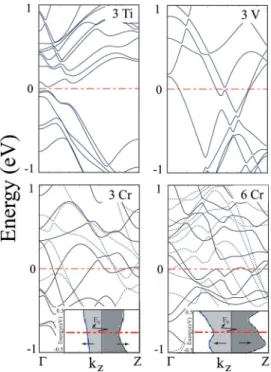
Calculated energy band structures of 共3,0兲+V, 共3,3兲 + Ti, 共3,3兲+3 Cr, and 共3,3兲+6 Cr are presented in Fig. 7. The 共3,0兲+V structure is a metal. Six bands crossing the Fermi level yield quantum ballistic conductance of G = 6G0.
The partial density of states indicates that V-3d and Si-3p orbital character dominate the states at the Fermi level. The 共3,3兲+3 Ti structure is a semiconductor with a very narrow band gap. In the case of共3,3兲+3 Cr and 共3,3兲+6 Cr several majority共spin-up ↑兲 and minority 共spin-down ↓兲 bands are crossing the Fermi level. Hence both structures are metals with finite density of majority D共E=EF,↑兲 and minority
D共E=EF,↓兲 spin states at EF. However, D共E=EF,↑兲
− D共E=EF,↓兲 is significant. These properties, which also
de-pend on the decoration of the tubes, can be used in nanospin-tronic device applications. Recently Dumitrica et al.10 have
investigated the stabilization共3,0兲 zigzag and 共2,2兲 armchair SWSiNTs by various atoms共Zr, Sc, Ti, Cr, Fe, Ni, Be, and Co兲 axially placed inside the tube. However, they consider neither the magnetic ground state due to specific TM atoms nor the stabilization of tubes that have a relatively larger radius.
FIG. 6. Perspective and top共cross section兲 view of the fully relaxed V doped共3,0兲, Ti-doped, and Cr-doped 共3,3兲 SWSiNTs. Our results revealed that small radius SWSiNTs can be stabilized by a doping transition metal element.
VI. OTHER TUBULAR STRUCTURES OF SILICON
We now consider different tubular structures which are formed by the stacking of atomic polygons as presented in Fig. 8. Three tubular structures given in the first row, i.e., T1,
T2, T3, are made of triangles of silicon atoms, which are
stacked along the axis of the tube. In T1, triangles are iden-tical and placed in a top-to-top共or eclipsed兲 position; in T2
the triangles are staggered; a T3 structure is constructed by
the insertion of a Si linear chain共Si-LC兲 into the T1structure
as such that the chain atoms are centered in between the layers. The same convention is followed in labeling the tu-bular silicon nanowires with pentagonal 共P1, P2, P3兲 and
hexagonal共H1, H2, H3兲 cross sections.
Starting with those geometries, structural optimizations in large supercells yielded T2, T3, and H3 as unstable, which
deformed into clusters. The structural parameters, the bind-ing energies, and equilibrium conductance values of stable tubular structures are summarized in Table I. All the stable silicon tubes have comparable binding energy values, with the P1 structure being slightly more favorable energetically.
Also within each set of tubular structures the top-to-top ar-rangement provides the highest cohesive energy. In Fig. 9 the energy band structure and equilibrium conductance plots of
T1, P1, and H1structures are presented. All of them are found
metallic with calculated ideal conductance values of 6G0,
10G0, and 6G0, respectively. A common feature noticed in the energy band structures of T1, P1, and H1 tubes is that there are almost filled bands available in close vicinity of the Fermi levels, which may lead to drastic conductance
varia-tions due to small structural perturbavaria-tions in the tubes or small bias voltage.
Earlier, the pentagonal nanowires of Si and also those of several metals such as Na, Al, Cu, Pb, Au, Fe, Ni, and Xe were investigated by Sen et al.59 using similar calculation
methods. The results for a specific structure, P3, which is
common in both studies, is in agreement. The stability of the
P3is further strengthened by the finite-temperature ab initio
molecular dynamics calculation carried out in the present study. Recently, Bai et al.60 have studied the stability of in-finite and in-finite S1共top-to-top square兲, P1 and H1 structures
by performing ab initio calculations using different methods, including pseudopotential plane waves and classical
molecu-FIG. 7.共Color online兲 The energy band structures of 共3,0兲+V, 共3,3兲+3 Ti, 共3,3兲+3 Cr, and 共3,3兲+6 Cr calculated by using the self-consistent-field spin-polarized GGA method. Solid lines and dotted lines are for majority and minority states, respectively. The inset shows the density of majority共dark兲 and minority 共light兲 spin states at the Fermi level of共3,3兲+3 Cr and 共3,3兲+6 Cr structures.
FIG. 8. Some tubular structures of Si. The tubes are formed by the stacking of Si polygons; the labels T, P, and H stand for trian-gular, pentagonal, and hexagonal configurations, respectively. T1, P1, and H1tubes have top-to-top arrangement of layers. In T2, P2, and H2the layers are staggered. T3, P3, and H3structures have extra
atoms centered in between the layers.
TABLE I. Structural and conductance properties of silicon tu-bular structures that are found stable. Ebis the binding energy per
atom, c is the unit cell length of the periodic structure, and d is the in-plane bond lengths of the polygonal atomic layers. Equilibrium conductance values are given by G in units of conductance quan-tum, Go= 2e2/ h.
Structure Eb共eV兲 c共Å兲 d共Å兲 G共2e2/ h兲
T1 4.62 2.37 2.38 6 T2 T3 P1 4.79 2.37 2.37 10 P2 4.68 2.70 2.46 10 P3 4.66 4.10 2.58 6 H1 4.77 2.29 2.37 6 H2 4.74 2.52 2.42 9 H3
lar dynamics calculations at 2000 K. Their stability analysis for P1and H1are in agreement with present results. In addi-tion to P1 and H1, the present study deals with T1 and also
staggered ones.
VII. SINGLE-WALL NANOTUBES OF III-V COMPOUNDS
Motivated by interesting properties of SW共BN兲NT and opto-electronic and field emitting properties of GaN and AlN tubular forms,21,25 we choose 共8,0兲 AlP, GaAs, and GaN
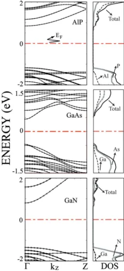
single-wall nanotubes as prototypes to investigate the stabil-ity and electronic properties of III-V compound nanotubes. Even if the single-wall nanotubes of these compounds have not been sythesized yet, the predictions of the present work are essential for further efforts to achieve. The initial bond lengths are chosen as the distance between nearest cation and anion atoms in bulk structure. After relaxation of all atomic positions, as well as lattice constant c, the tubular structures remained stable. The ab initio MD calculations also showed that SW共AlP兲NT remained stable at room temperature after 250 time steps. Eb is calculated to be 9.6 eV per AlP basis.
The radius of the tube is 5.2 Å. The structure is not a perfect tube but the hexagons on the surface are buckled. The near-est Al– P distance is 2.3 Å, and second nearnear-est-neighbor dis-tance i.e., nearest P – P and Al– Al disdis-tances, are 3.9 Å and 3.8 Å, respectively. The energy band and TDOS analysis in Fig. 10 points out that共8,0兲 SW共AlP兲NT is a semiconductor 共insulator兲 with a band gap of 2.0 eV.
Initial tubular structure of 共8,0兲 SW共GaAs兲NT is main-tained after geometry optimization at T = 0 K. Similar to SW共AlP兲NT, hexagons are buckled. Eb is calculated to be
7.7 eV per GaAs and the radius is 4.8 Å. The nearest Ga– As distance is 2.4 Å, and the nearest Ga– Ga and As– As
dis-tances are 3.9 Å and 4.1 Å, respectively. The 共8,0兲 SW共GaAs兲NT is also a semiconductor 共insulator兲 with a band gap of 0.9 eV.
We place a special emphasis on GaN nanotubes,20,61
which are successfully synthesized by an epitaxial casting method where ZnO nanowires are initially used as templates. GaN nanotubes produced this way have a diameter of 300 Å and a minimum wall thickness of 50 Å. They are semicon-ducting and hence they would be a possible candidate for opto-electronic applications. Whether a single-wall GaN tube of smaller diameter 共2R⬃10 Å兲 can be stable and can ex-hibit technologically interesting electronic properties is im-portant to know. We again took共8,0兲 SW共GaN兲NT as a pro-totype for the sake of consistency. Stable tubular geometry is obtained by both geometry optimization at T = 0 K and ab
initio MD analysis at T = 800 K. Upon relaxation, atoms on
the surface are buckled. Eb is calculated to be 11.5 eV per
GaN and the radius is 4.1 Å. The nearest Ga– N distance is 1.8 Å, and the nearest Ga– Ga and N – N distances are 3.1 Å and 3.2 Å, respectively. We found that the 共8,0兲
FIG. 9.共Color online兲 Energy band structure of Si tubular struc-tures formed by the top-to-top stacking of triangular共T1兲,
pentago-nal共P1兲, and hexagonal 共H1兲 polygons. In the right panels the cor-responding equilibrium conductance in Go= 2e2/ h curves are
plotted. The Fermi levels are set to zero.
FIG. 10. 共Color online兲 Energy band structures 共left panels兲, TDOS, and partial density of states on atoms共right panels兲 of 共8,0兲 zigzag SW共AlP兲NT, SW共GaAs兲NT, and SW共GaN兲NT. Anion 共Al, Ga兲 and cation 共P, As, N兲 contributions to TDOS are shown by dashed and light continuous lines. Zero of the energy is set at the Fermi level.
SW共GaN兲NT is a semiconductor 共insulator兲 with a band gap of 2.2 eV. A previous first-principles study performed by Lee
et al.23 by using a LDA method predicted the similar band
gap for SW共GaN兲NT. Here, we examine also whether SW共GaN兲NT is radially elastic. To this end we started with the elliptically deformed nanotube under⑀yy= −0.1 and let it
relax in the absence of radial forces. Similar to the Si nano-tube, SW共GaN兲NT is found to be radially soft.
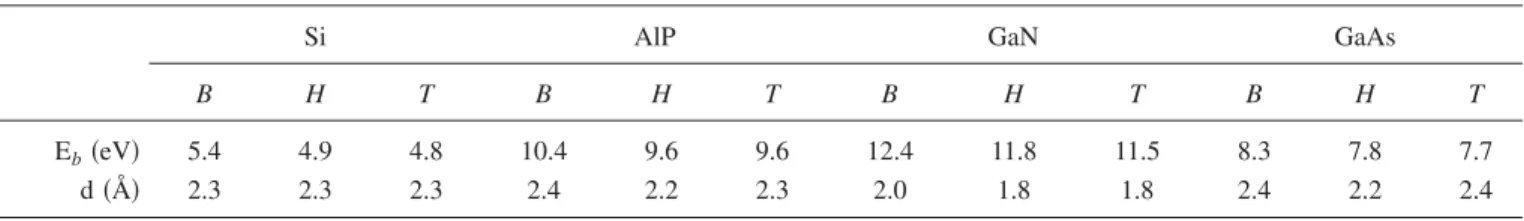
For the sake of comparison, the binding energy and bond distance of bulk crystals, honeycomb structures, and 共8,0兲 tubular structures of Si, AlP, GaN, and GaAs are presented in Table II. In these structures the covalent or共covalent-ionic兲 mixed bonds have different orbital combinations. While bulk crystals are tetrahedrally coordinated and have bonds formed by sp3-hybrid orbitals, in honeycomb and tubular structures bonding through sp2-hybrid orbitals dominates the cohesion.
VIII. CONCLUSION
In this paper, we analyzed the stability of Si and III-V compound, single-wall nanotubes, and calculated their opti-mized atomic structure and energy band structure. Si as well as III-V compounds can form a stable 2D honeycomb struc-ture, which is precursor of nanotubes. The energy necessary to roll these honeycomb structures over a cylinder of radius
R to make a perfect nanotube is small, however, as compared
to those in carbon nanotubes. We found that Si single-wall nanotubes with small radius are unstable and are clustered either at T = 0 K or at finite temperatures. For example, while 共3,0兲 is unstable even at T=0 K, 共4,0兲 and 共5,0兲 lose their tubular character and tend to form cluster at T = 500 K. Stable共n,0兲 zigzag SWSiNTs are metallic for 6艋n艋11, but become semiconducting for n艋12. The metallicity of small radius 共n,0兲 tubes is a typical curvature effect and results from the dipping of the singlet*band into the valence band
at small radius. Stable共n,n兲 armchair SWSiNTs 共n=6,9兲 are metallic. Our study on radially deformed 共8,0兲 and 共6,6兲 SWSiNTs demonstrated that these nanotubes are radially “soft,” and hence are devoid of the strong restoring force that maintains radial elasticity. The radial softness of Si tubes is a behavior which distinguishes them from carbon nanotubes. In contrast to that axial stiffness the Si nanotube has been found to be high. We predicted that oxygen molecules ad-sorbed on the Si– Si bonds dissociates. A strong interaction between O / O2 and SWSiNT appears to be serious in future
processes involving Si tubes. Adatoms like Si, Au, and H can also form strong chemisorption bonds with the atoms on the surface of SWSiNT. We showed that unstable, small radius SWSiNTs can be stabilized through the implementation or external adsorption of 3d transition metal atoms. In particu-lar, the decoration of the tube surface by the external adsorp-tion of transiadsorp-tion metal atoms can lead to magnetic proper-ties, which may find potential technological applications. Small radius tubular structures different than those based on the honeycomb structure have been identified. Finally, we found III-V compound 共8,0兲 nanotubes 共AlP, GaAs, and GaN兲 stable at least at room temperature and they are semi-conductors with band gaps ranging from 0.9 eV to 2.2 eV. In contrast to small radius metallic Si nanotubes, 共8,0兲 com-pound nanotubes are semiconductors. The band gap in-creases with a decreasing row number of elements. Even though not all the structures treated in this study have been realized experimentally, the predictions obtained from the present first-principles calculations are expected to be essen-tial for further research in this field.
ACKNOWLEDGMENTS
Part of the computations has been carried out at ULAK-BIM Computer Center. S.C. acknowledges partial financial support from Academy of Science of Turkey.
*Corresponding author.
Electronic address: [email protected]
1S. Iijima, Nature共London兲 354, 56 共1991兲; S. Iijima, T. Ichihashi,
and Y. Ando, Nature共London兲 356, 776 共1992兲.
2M. S. Dresselhaus, G. Dresselhaus, and P. C. Eklund, Science of Fullerenes and Carbon Nanotubes共Academic, San Diego, CA,
1996兲.
3R. Saito, G. Dresselhaus, and M. S. Dresselhaus, Physical Prop-erties of CarbonNanotubes共Imperial College, London, 1998兲. 4J. W. Mintmire, B. I. Dunlap, and C. T. White, Phys. Rev. Lett.
68, 631共1992兲.
5For the most recent review on the functionalization and the
elec-tronic properties of single-wall carbon nanotubes and for addi-tional references, see, for example, S. Ciraci, T. Yildirim, S. Dag, O. Gülseren, and R. T. Senger, J. Phys.: Condens. Matter
16, R901共2004兲.
6S. B. Fagan, R. J. Baierle, R. Mota, A. J. R. da Silva, and A.
Fazzio, Phys. Rev. B 61, 9994共1999兲.
7S. B. Fagan, R. Mota, R. J. Baierle, G. Paiva, A. J. R. da Silva,
and A. Fazzio, J. Mol. Struct.: THEOCHEM 539, 101共2000兲. TABLE II. Calculated binding energies Eband bond distances d in Å of various structures of Si, AlP, GaAs, and GaN. B is a 3D bulk
crystal, H is a 2D honeycomb structure, and T is the共8,0兲 single-wall nanotube structure. The units of binding energy are eV/atom for Si and eV/basis for III-V compounds.
Si AlP GaN GaAs
B H T B H T B H T B H T
Eb共eV兲 5.4 4.9 4.8 10.4 9.6 9.6 12.4 11.8 11.5 8.3 7.8 7.7
8A. S. Barnard and S. P. Russo, J. Phys. Chem. B 107, 7577
共2003兲.
9V. V. Ivanovskaya, A. A. Sofronov, and A. L. Ivanosvkii, Phys.
Lett. A 297, 436共2002兲.
10T. Dumitrica, M. Hua, and B. I. Yakobson, Phys. Rev. B 70,
241303共R兲 共2004兲.
11O. Ponomarenko, M. W. Radny, and P. V. Smith, Surf. Sci. 562,
257共2004兲.
12M. Zhang, Y. H. Kan, Q. J. Zang, Z. M. Su, and R. S. Wang,
Chem. Phys. Lett. 379, 81共2003兲.
13R. Q. Zhang, S. T. Lee, C. K. Law, W. K. Li, and B. K. Teo,
Chem. Phys. Lett. 364, 251共2002兲.
14G. Seifert, Th. Köhler, K. H. Urbassek, E. Hernàndez, and Th.
Frauenheim, Phys. Rev. B 63, 193409共2001兲.
15A. K. Singh, T. M. Briere, V. Kumar, and Y. Kawazoe, Phys. Rev.
Lett. 91, 146802共2003兲.
16B. Marsen and K. Sattler, Phys. Rev. B 60, 11593共1999兲. 17J. Sha, J. Niu, X. Ma, J. Xu, X. Zhang, Q. Yang, and D. Yang,
Adv. Mater.共Weinheim, Ger.兲 14, 1219 共2002兲; J. Niu, J. Sha, and D. Yang, Physica E共Amsterdam兲 23, 131 共2004兲.
18A. Loiseau, F. Willaime, N. Demoncy, G. Hug, and H. Pascard,
Phys. Rev. Lett. 76, 4737共1996兲; J. S. Lauret, R. Arenal, F. Ducastelle, A. Loiseau, M. Cau, B. Attal-Tretout, E. Rosencher, and L. Goux-Capes, Phys. Rev. Lett. 94, 037405共2005兲.
19Z. Liliental-Weber, Y. Chen, S. Ruvimov, and J. Washburn, Phys.
Rev. Lett. 79, 2835共1997兲.
20J. Goldberger, R. He, Y. Zhang, S. Lee, H. Yan, H. Choi, and P.
Yang, Nature共London兲 422, 599 共2003兲.
21V. N. Tondare, C. Balasubramanian, S. Shende, D. S. Joag, V. P.
Godbale, and S. V. Bhoraskar, Appl. Phys. Lett. 80, 4813 共2002兲.
22A. Rubio, J. L. Corkill, and M. L. Cohen, Phys. Rev. B 49,
R5081共1994兲.
23S. M. Lee, Y. H. Lee, Y. G. Hwang, J. Elsner, D. Porezag, and T.
Frauenheim, Phys. Rev. B 60, 7788共1999兲.
24M. Cote, M. L. Cohen, and D. J. Chadi, Phys. Rev. B 58, R4277
共1998兲.
25M. Zhao, Y. Xia, D. Zhang, and L. Mei, Phys. Rev. B 68, 235415
共2003兲.
26L. Rapoport, Y. Bilik, Y. Feldman, M. Homyonfer, S. R. Cohen,
and R. Tenne, Nature共London兲 387, 791 共1997兲.
27Y. Feldman, E. Wasserman, D. J. Srolovitz, and R. Tenne, Science
267, 222共1995兲.
28R. Tenne, L. Margulis, M. Genut, and G. Hodes, Nature共London兲
360, 444共1992兲.
29Y. R. Hacohen, E. Grunbaum, R. Tenne, J. Sloand, and J. L.
Hutchinson, Nature共London兲 395, 336 共1998兲.
30M. C. Payne, M. P. Teter, D. C. Allen, T. A. Arias, and J. D.
Joannopoulos, Rev. Mod. Phys. 64, 1045共1992兲.
31Numerical computations have been carried out by using VASP
software: G. Kresse and J. Hafner, Phys. Rev. B 47, R558 共1993兲; G. Kresse and J. Furthmuller, Phys. Rev. B 54, 11169 共1996兲.
32W. Kohn and L. J. Sham, Phys. Rev. 140, A1133 共1965兲; P.
Hohenberg and W. Kohn, Phys. Rev. 136, B864共1964兲.
33D. Vanderbilt, Phys. Rev. B 41, R7892共1990兲.
34J. P. Perdew, J. A. Chevary, S. H. Vosko, K. A. Jackson, M. R.
Pederson, D. J. Singh, and C. Fiolhais, Phys. Rev. B 46, 6671 共1992兲.
35M. Methfessel and A. T. Paxton, Phys. Rev. B 40, 3616共1989兲.
36H. J. Monkhorst and J. D. Pack, Phys. Rev. B 13, 5188共1976兲. 37For an extensive discussion of the GW method: F. Aryasetiawan
and O. Gunnarsson, Rep. Prog. Phys. 61, 237共1998兲.
38T. Miyake and S. Saito, Phys. Rev. B 68, 155424共2003兲. 39C. D. Spataru, S. Ismail-Beigi, L. X. Benedict, and S. G. Louie,
Phys. Rev. Lett. 92, 077402 共2004兲; Appl. Phys. A 78, 1129 共2004兲.
40Y. Ouyang, J. Huang, C. L. Cheung, and C. M. Lieber, Science
292, 702共2001兲.
41O. Gülseren, T. Yildirim, and S. Ciraci, Phys. Rev. B 65, 153405
共2002兲.
42S. Nosé, Mol. Phys. 52, 255–268共1984兲.
43U. Röthlisberger, W. Andreoni, and M. Parrinello, Phys. Rev.
Lett. 72, 665共1994兲.
44K. Takeda and K. Shiraishi, Phys. Rev. B 50, 14916共1994兲. 45The same problem, as well as the energetics of graphite by itself
have been treated by Y. C. Wang, K. Scheerschmidt, and U. Gosele, Phys. Rev. B 61, 12864共2000兲. In this paper, the inter-action energies of physisorption and chemisorption states are equal for a fixed lattice parameter a = 3.86 Å. However, the re-sults indicate that a should differ by going from physisorption to chemisorption. We also found that planar Si layers are buckled and the energy difference between␣ and  configuration is only 100 meV.
46J. C. Charlier, X. Gronze, and J. P. Michenoud, Europhys. Lett.
28, 4040共1994兲.
47W. Kohn, Y. Meir, and D. E. Makarov, Phys. Rev. Lett. 80, 4153
共1998兲.
48S. Dag, O. Gülseren, T. Yildirim, and S. Ciraci, Phys. Rev. B 67,
165424共2003兲.
49Z. K. Tang et al., Science 292, 2462共2001兲.
50N. Wang, Z. K. Tang, G. D. Li, and J. S. Chen, Nature共London兲
408, 50共2000兲.
51E. Durgun, S. Dag, V. K. Bagci, O. Gülseren, T. Yildirim, and S.
Ciraci, Phys. Rev. B 67, 201401共R兲 共2003兲; E. Durgun, S. Dag, S. Ciraci, O. Gülseren, J. Phys. Chem. B 108共2兲, 575 共2004兲.
52D. H. Robertson, D. W. Brenner, and J. W. Mintmire, Phys. Rev.
B 45, R12592共1992兲; G. G. Tibbets, J. Cryst. Growth 66, 632 共1984兲; K. N. Kudin, G. E. Scuseria, and B. I. Yakobson, Phys. Rev. B 64, 235406共2001兲.
53T. W. Tombler, C. W. Zhou, L. Alexseyev, J. Kong, H. J. Dai, L.
Lei, C. S. Jayanthi, M. J. Tang, and S. Y. Wu, Nature共London兲 405, 769共2000兲.
54P. Zhang, P. E. Lammert, and V. H. Crespi, Phys. Rev. Lett. 81,
5346共1998兲.
55O. Gülseren, T. Yildirim, S. Ciraci, and C. Kilic, Phys. Rev. B 65,
155410共2002兲.
56C. Kilic, S. Ciraci, O. Gülseren, and T. Yildirim, Phys. Rev. B 62,
R16345共2000兲.
57D. Sanchez-Portal, E. Artacho, J. M. Soler, A. Rubio, and P.
Ordejon, Phys. Rev. B 59, 12678共1999兲.
58X. Blase, L. X. Benedict, E. L. Shirley, and S. G. Louie, Phys.
Rev. Lett. 72, 1878共1994兲.
59P. Sen, O. Gulseren, T. Yildirim, I. P. Batra, and S. Ciraci, Phys.
Rev. B 65, 235433共2002兲.
60J. Bai, X. C. Zang, H. Tanaka, and J. Y. Zang, Proc. Natl. Acad.
Sci. U.S.A. 101, 2664共2004兲.
61M. W. Lee, H. C. Hsueh, H.-M. Lin, and C.-C. Chen, Phys. Rev.