Buried Waveguides Written Deep inside Silicon
Ahmet Turnali1, Onur Tokel1,2, Denizhan Koray Kesim1, Ghaith Makey1,2, Parviz Elahi1,2, Fatih Ömer Ilday1,2
1. Department of Electrical and Electronics Engineering, Bilkent University, 06800, Ankara, Turkey 2. Department of Physics, Bilkent University, 06800, Ankara, Turkey
Silicon waveguides are widely used as optical interconnects and they are particularly important for Si-photonics. Si-based devices, along with other optical elements, are entirely fabricated on the top surface of Si wafers. However, further integration of photonic and electronic devices in the same chip requires a new approach. One alternative is to utilize the bulk of the wafer for fabricating photonic elements. Recently, we reported a direct-laser-writing method that exploits nonlinear interactions and can generate subsurface modifications inside silicon without damaging the surface [1]. Using this method, we fabricated several functional optical elements including gratings [1], lenses [2], and holograms [3]. In this work, we demonstrate optical waveguides entirely embedded in Si.
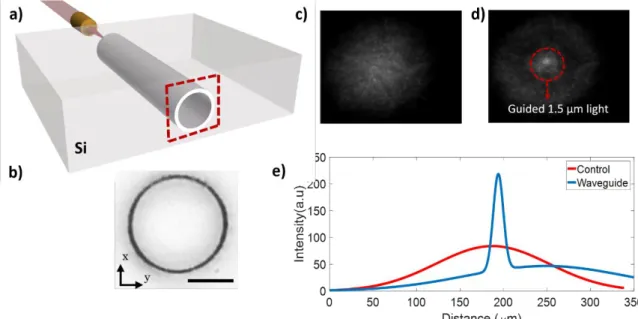
Fig. 1. a) Schematic of subsurface waveguide inscription. Modified regions which has smaller refractive index compared to
crystal silicon are used as cladding for waveguiding. b) Infrared microscope image of a representative tubular modification written inside Si. Scale bar is 25 µm. c) Far-field image from unprocessed silicon as control experiment. d) Far-field image from the output of the subsurface waveguide. e) Intensity profile of the recorded images compared for the waveguide (blue curve), and control experiment (red curve). Increase in the intensity is an indication of waveguiding.
In order to fabricate subsurface waveguides, we used a home-made master oscillator power amplifier (MOPA) system that operates at 1.55 µm and produces 5-ns pulses at 150 kHz repetition rate. We used longitudinal writing scheme for fabrication (Fig.1.a). We determined refractive index of the modified regions with respect to unmodified crystal by direct phase difference calculation through interference measurements. We measured a refractive index change in the order of 10-4. In addition, the refractive index change was observed to be negative, i.e., a tubular type geometry is needed for waveguide operation. For experiments, we fabricated 2.5-mm long waveguides with 20-µm diameter (Fig.1.b). During the characterization of waveguides, we used a collimated continuous wave (CW) laser operating at 1.55 µm as a light source. We coupled the light with a NA = 0.68 lens into waveguide. The same setup was used for the control experiments, where we directed light into unprocessed silicon under the same conditions. The far-field images and intensity profile comparison is given Fig.1.c- 1.e. Intensity increase when light is coupled to modified region is confirmation of waveguiding.
In summary, we have used nonlinear laser lithography to write a tubular waveguide geometry buried inside silicon without damaging the chip surface, and successfully confirmed waveguiding in the bulk of Si. The waveguide can be positioned at any desired position inside the wafer.
References
1 O. Tokel, A. Turnali, I. Pavlov, S. Tozburun, I. Akca, and F. O. Ilday, “Laser-Writing in Silicon for 3D Information Processing,” arXiv.org, vol. physics.optics. 09-Sep-2014.
2 A. Turnali, O. Tokel, I. Pavlov, and F. Ö. Ilday, “Direct laser writing of volume fresnel zone plates in silicon,” 2015 European Conference on Lasers and Electro-Optics - European Quantum Electronics Conference (2015), paper CM_4_5, p. CM_4_5, Jun. 2015. [3] A. Turnali, O. Tokel, G. Makey, I. Pavlov, and F. Ö. Ilday, “Computer-generated holograms embedded in bulk silicon with nonlinear laser lithography,” 2016 Conference on Lasers and Electro-Optics (2016), paper STh1Q.7, Jun. 2016.