INVESTIGATION OF THE MAGNETIC
PROPERTIES OF BSCCO
SUPERCONDUCTORS WITH SCANNING
HALL PROBE MICROSCOPE
a thesis
submitted to the department of physics
and the institute of engineering and science
of b˙ilkent university
in partial fulfillment of the requirements
for the degree of
master of science
By
M¨
unir Dede
September, 2002
I certify that I have read this thesis and that in my opinion it is fully adequate, in scope and in quality, as a thesis for the degree of Master of Science.
Assoc. Prof. Dr. Ahmet Oral (Supervisor)
I certify that I have read this thesis and that in my opinion it is fully adequate, in scope and in quality, as a thesis for the degree of Master of Science.
Assoc. Prof. Dr. Recai M. Ellialtıo˘glu
I certify that I have read this thesis and that in my opinion it is fully adequate, in scope and in quality, as a thesis for the degree of Master of Science.
Prof. Dr. Tezer Fırat
Approved for the Institute of Engineering and Science:
Prof. Dr. Mehmet Baray
Director of the Institute of Engineering and Science
ABSTRACT
INVESTIGATION OF THE MAGNETIC PROPERTIES
OF BSCCO SUPERCONDUCTORS WITH SCANNING
HALL PROBE MICROSCOPE
M¨unir Dede M.S. in Physics
Supervisor: Assoc. Prof. Dr. Ahmet Oral September, 2002
A low temperature scanning Hall probe microscope (LT-SHPM) with low noise GaAs/AlGaAs 2DEG Hall probes is used to investigate the magnetic properties of a Ag-sheathed BSCCO-2223 tape and a single crystal BSCCO-2212 supercon-ductor. The Hall probes are micro fabricated with 1 µm wide Hall bars which have ∼0.85 µm electrical width.
The magnetization behavior, vortex structures and the vortex lattice melting are observed at 77 K. Flux penetration into the BSCCO-2212 single crystal is also observed and imaged with single vortex resolution.
Keywords: Scanning Hall Probe Microscopy (SHPM), Hall probes, Magnetization measurement, Superconductivity, BSCCO, Single quantum flux.
¨
OZET
BSCCO T˙IP˙I S ¨
UPER˙ILETKENLER˙IN MANYET˙IK
¨
OZELL˙IKLER˙IN˙IN TARAMALI HALL AYGITI
M˙IKROSKOBU ˙ILE ˙INCELENMES˙I
M¨unir Dede Fizik, Y¨uksek Lisans
Tez Y¨oneticisi: Do¸c. Dr. Ahmet Oral Eyl¨ul, 2002
Bu tezde d¨u¸s¨uk sıcaklıkta ¸calı¸san bir Taramalı Hall Aygıtı Mikroskobu’nun (THAM) calı¸sma prensibi ve mikroskopta kullanılan Hall Aygıtı sens¨orlerinin ¨
uretimi anlatılmı¸stır.
Bu mikroskop BSCCO tipi s¨uper iletkenlerin manyetik ¨ozelliklerinin ¸calı¸sıl masında kullanılmı¸stir. Manyetik alan altındaki ind¨uklenme, ¨ozellikle akı gir-daplarının olu¸sumu ve erimesi incelenmi¸stir. Ba˘gımsız girdap yapıları tekil kuan-tum akı ¸c¨oz¨un¨url¨u˘g¨u ile resimlenmi¸stir.
Anahtar s¨ozc¨ukler : Taramalı Hall Aygıtı Mikroskobisi, Manyetizma, ¨Ust¨uniletkenlik, Tarama ucu, BSCCO, Tekil kuantum akı.
Acknowledgement
I would like to express my deep gratitude to my supervisor Assoc. Prof. Dr. Ahmet Oral, for his friendly attitude and guidance.
I debt special thanks to Assoc. Prof. Dr. Recai M. Ellialtıo˘glu and Prof. Dr. Tezer Fırat for the comments and corrections on the thesis.
I owe special thanks to Sinan Selcuk who cheered me up. I would like to thank also, Mehrdad Atabak, and M. Murat Kaval for their help and remarks.
Last but not the least, I wish to thank to my parents and my wife G¨ulden for the life they have provided for me.
Contents
1 Introduction 1
1.1 Organization of the Thesis . . . 6
2 Scanning Hall Probe Microscope 7 2.1 Hall Effect . . . 7
2.2 The Microscope . . . 11
2.2.1 The Microscope Body . . . 13
2.2.2 The Electronics and Computer Control Unit . . . 16
2.2.3 The LT-SHPM Specifications . . . 18
3 Hall Sensor Fabrication 20 3.1 Wafer Preparation for Microfabrication . . . 20
3.1.1 Wafer Rounding . . . 20
3.1.2 Sample Cleaning . . . 22
3.2 Hall Probe Etch . . . 22
3.3 Mesa Etch . . . 23 vi
CONTENTS vii
3.4 Recess Etch . . . 23
3.5 Ohmic Contact Metallization . . . 24
3.6 Tip Metallization . . . 24
3.7 Cleaving and Sensor mounting . . . 25
3.8 Characterization and Noise Measurement . . . 26
3.8.1 Gallium Arsenide (GaAs) Hall Sensors . . . 28
3.8.2 Indium Antimonide (InSb) Thin Film Hall Sensors . . . . 32
3.8.3 Other Materials . . . 35
4 Results 37 4.1 Preparation for Scan . . . 37
4.2 Ag-Sheathed Bi-2223 BSCCO Tape . . . 39
4.3 Single Crystal BSCCO-2212 . . . 50
List of Figures
1.1 The transition behavior of type 1 superconductors under externally
applied magnetic field. . . 2
1.2 The Meissner effect. . . 3
1.3 The transition behavior of type 2 superconductors under externally applied magnetic field. . . 4
1.4 Construction of vortices in type 2 superconductors. . . 4
2.1 Schematic description of Hall effect . . . 8
2.2 Schematic description of the Scanning Hall Probe Microscope . . 12
2.3 The LT-SHPM . . . 13
2.4 Piezoelectric scanner tube . . . 15
2.5 Description of scan method of the scanner tube . . . 16
2.6 The electronic control unit . . . 17
3.1 A corner of the rounded chip before the photolithography. . . 21
3.2 Finished Hall probe sensor mounted on a PCB chip holder. . . 25 3.3 Noise spectrum of the GaAs Hall probe for 2.5 µA current at 300 K. 28
LIST OF FIGURES ix
3.4 The minimum detectable magnetic field as a function of Hall cur-rent at 300 K for GaAs Hall probe . . . 29 3.5 The minimum detectable magnetic field as a function of Hall
cur-rent at 77 K for GaAs Hall probe. . . 30 3.6 Voltage noise as a function of Hall current at 77 K for GaAs Hall
probe. . . 30 3.7 The voltage noise spectrum of GaAs Hall probe at 77 K for IHall=10
µA. . . 31 3.8 The voltage noise spectrum of GaAs Hall probe at 77 K for IHall=20
µA. . . 31 3.9 The minimum detectable magnetic field as a function of current at
300 K with InSb Hall sensor (Hall bar size=1 µm). . . 33 3.10 The minimum detectable voltage as a function of current at 300 K
with InSb Hall sensor (Hall bar size=1 µm). . . 33 3.11 The minimum detectable magnetic field as a function of current at
300 K with InSb Hall sensor (Hall bar size=12 µm). . . 34 3.12 The minimum detectable voltage as a function of current at 300 K
with InSb Hall sensor (Hall bar size=12 µm). . . 34 3.13 25 µm × 25 µm RT-SHPM images of 5.5 µm thick crystalline
bismuth-substituted iron garnet films obtained with Hall currents of (a) 3, (b) 30, and (c) 50 µA [15]. . . 35
4.1 Experimental setup . . . 38 4.2 The BSCCO tape and the estimated scanned region. . . 39 4.3 The SHPM image and cross section taken after externally applied
LIST OF FIGURES x
4.4 The SHPM image and cross section taken after externally applied
varying, only + 138 Oe external magnetic field and back to zero. . 41
4.5 The magneto optical Bz and Jc images of the tape [20]. . . 42
4.6 BH curves taken diagonally. . . 43
4.7 The BH curve at the point A. . . 43
4.8 The BH curve at the point B. . . 44
4.9 The BH curve at the point C. . . 44
4.10 The BH curve at the point D. . . 45
4.11 The BH curve at the point E. . . 45
4.12 The BH curve at the point F. . . 46
4.13 The BH curve at the point G. . . 46
4.14 The BH curve at the point H. . . 47
4.15 The BH curve at the point I. . . 47
4.16 The BH curve at the point J. . . 48
4.17 The BH curve at the point K. . . 48
4.18 SHPM image of overlapped vortices, the figure histogram of the image and the crossections. . . 49
4.19 LT-SHPM image of individual vortices with single quantum flux resolution at 77 K . . . 52
4.20 LT-SHPM image of chain like alignment of vortices at 77K . . . . 53
4.21 The cross sections of the vortices . . . 54
LIST OF FIGURES xi
4.23 BH curve measured at 77K . . . 56 4.24 The lattice melting transition on MH curve. . . 56 4.25 LT-SHPM real time images of anti-vortex penetrating into
BSCCO-2212 single crystal at 77 K. . . 57 4.26 LT-SHPM real time images of vortex penetrating into
List of Tables
3.1 The specifications of GaAs Hall sensors at 77K . . . 36 3.2 The specifications of InSb Hall sensors at 300K . . . 36
4.1 The scan parameters of the SHPM image shown in Fig.4.3 and 4.4 50 4.2 The scan parameters of the SHPM image shown in Fig.4.18 . . . 50 4.3 The scan parameters of the LT-SHPM image shown in Fig.4.19 . 52 4.4 The scan parameters of the LT-SHPM image shown in Fig.4.20 . 53
Chapter 1
Introduction
Study of structural and magnetic properties of materials are of general interest for improved understanding of magnetism and for tailoring the properties of new magnetic materials and superconductors.
Superconductors are elements like, Pb, Nb or inter-metallic alloys, or com-pounds that will conduct electricity without resistance below a certain tempera-ture. However, this applies only to direct electric current (DC), to finite amounts of current and external magnetic fields. In other words, superconducting state is defined by three factors: critical temperature (Tc), critical field (Hc), and critical
current density (Jc). Each of these parameters is very dependant on the other
two properties present.
Maintaining the superconducting state requires that both the magnetic field and the current density, as well as the temperature, remain below the critical val-ues, all of which depend on the material. Below the superconducting transition temperature, the resistivity of a material is exactly zero. Since there is no loss in electrical energy when superconductors carry electrical current, relatively nar-row wires made of superconducting materials can be used to carry huge currents. However, there is a certain maximum current that these materials can be made to carry, above which they stop being superconductors. If too much current is pushed through a superconductor, it will revert to the normal state even though
CHAPTER 1. INTRODUCTION 2
it may be below its transition temperature. The value of critical current density, Jc, is a function of temperature; i.e., the colder you keep the superconductor
the more current it can carry. Superconductivity is a macroscopic quantum
..
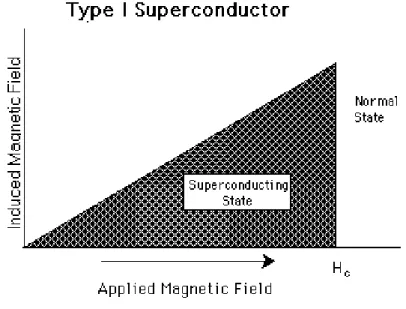
Figure 1.1: The transition behavior of type 1 superconductors under externally applied magnetic field.
phenomenon and these materials are classified as type 1 and type 2. A type 1 superconductor (Fig. 1.1) will push the externally applied magnetic field out of itself when the temperature is lowered to below the critical temperature, Tc as
illustrated in Fig.1.2. It does this by creating surface currents in itself which produces a magnetic field exactly countering the external field. The supercon-ductor becomes perfectly diamagnetic, cancelling all magnetic flux in its interior. This perfect diamagnetic property of superconductors is perhaps the most funda-mental macroscopic property of a superconductor and is referred as the Meissner Effect. If the magnetic field is increased to a given point the superconductor will go to the normal resistive state.
Type 2 superconductors however, differ from type 1 in that their transition from a normal to a superconducting state is gradual across a region of mixed state
CHAPTER 1. INTRODUCTION 3
..
Figure 1.2: The Meissner effect.
behavior as shown in Fig 1.3. This mixed phase helps to preserve superconduc-tivity between Hc1 to Hc2 which is the vortex state and describes the circulation
of supercurrent in vortices throughout the the specimen.
Such materials can be subjected to much higher external magnetic fields and currents without destroying their superconductivity. These high magnetic field and current values depend upon two important parameters which influence en-ergy minimization, penetration depth and coherence length. Penetration depth is the characteristic length of the fall off of a magnetic field due to surface currents. Coherence length is a measure of the shortest distance over which superconduc-tivity may be established. The ratio of penetration depth to coherence length is known as the Ginzburg-Landau parameter. If this value is greater than 0.7, complete flux exclusion is no longer favorable and flux is allowed to penetrate the superconductor through cores known as vortices. Thus, the magnetic field is not excluded completely, but is constrained in filaments within the material in the form of individual magnetic flux quanta, Φ0 (Fig. 1.4).
It is very important that the vortices do not move in response to magnetic fields if superconductors are to carry large currents. Vortex movement results in resistivity. Vortex movement can be effectively pinned at sites of atomic defects,
CHAPTER 1. INTRODUCTION 4
..
Figure 1.3: The transition behavior of type 2 superconductors under externally applied magnetic field.
..
CHAPTER 1. INTRODUCTION 5
such as inclusions, impurities, and grain boundaries. Pinning sites can be inten-tionally introduced into superconducting material by the addition of impurities.
Knowing how the vortices move and arrange themselves under various tem-perature and magnetic-field conditions, as well as how these phenomena are influ-enced by the physical properties of the material, will be critical in controlling the flux motion and maintaining the supercurrent flow in these materials. This could lead to a better understanding of the basic phenomena of superconductivity; and it could provide ways to improve the magnetic quality of the presently known materials by enhancing flux pinning in a controllable manner.
Characterization of the surface stray film distributions and flux pinning ar-rays done by magnetically sensitive microscopy techniques. Magnetic sensitive microscopy techniques provide valuable information about micro magnetic con-figuration [1], such as magnetic domain and domain wall structures down to sub-micron scale. By these techniques even surface spin structures at the atomic level are accessible.[2]
Many different techniques are employed for this purpose including the scan-ning Hall probe microscopy (SHPM)[3-5], the scanscan-ning quantum interference device (SQUID)microscope [6, 7], the magnetic force microscopy (MFM)[8, 9], Faraday rotation [10], Bitter decoration [11] and Magneto optical imaging [12] . Among the local magnetic probes listed above, MFM has the highest spatial reso-lution, ∼20-30 nm., but the detected signal is difficult to quantify. Moreover, the technique has a high self field that can disturb the local magnetic fields near the surface. On the other hand SQUID has high magnetic field resolution, however its spatial resolution is limited[13].
Thus SHPM becomes superior to other techniques by combining the high mag-netic and spatial resolution capabilities and non invasiveness, and its operation flexibility under a wide range of temperature and external magnetic fields.
CHAPTER 1. INTRODUCTION 6
1.1
Organization of the Thesis
The thesis is organized as follows: Chapter 2 introduces the basic principles of the low temperature scanning Hall probe microscope and the underlying physical phenomenon. Some features of the microscope system is also given. In Chapter 3, the micro fabrication, and the typical characteristics of the Hall probes are described. In addition to this, noise and its measurement are presented in this chapter with specific examples. In chapter 4, the experimental procedure and experimental results are discussed in detail. Finally, Chapter 5 concludes the thesis.
Chapter 2
Scanning Hall Probe Microscope
Scanning Hall probe microscope is a member of the family of microscopes named Scanning Probe Microscopes (SPMs). These are instruments used for studying various surface properties of materials, from the micrometer scale to the atomic scale in a wide range of disciplines.
Thus, SHPM contains the common properties of these instruments even if the detection technique may differ. In this chapter, these common features and the physical phenomenon used for the detection mechanism are explained.
2.1
Hall Effect
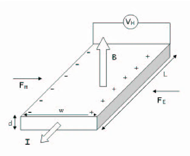
Hall effect is named after Edward H. Hall, who discovered the effect in 1878 during a study of the force acting on a current carrying metal in a magnetic field. The Hall effect gained an important place in the history of science and in-dustry by providing accurate and easy measurement of carrier density, electrical resistivity, and the mobility of carriers in semiconductors and metals.
Hall’s discovery showed that when a current carrying conductor is placed in an external magnetic field perpendicular to the direction of the applied current flow,
CHAPTER 2. SCANNING HALL PROBE MICROSCOPE 8
..
Figure 2.1: Schematic description of Hall effect
a voltage difference is developed across the material as shown in Fig. 2.1. This is called the Hall voltage and the developed electric field (−→E ) is perpendicular to the applied magnetic field and the direction of current.
The Hall effect is analogous to the magnetic deflection of an electron beam in a cathode ray tube. The physical principle is the well known Lorenz force;
−
→F = q−→υ ×−→B (2.1) acting on a charged particle. When a charge carrier moves along a direction perpendicular to an applied magnetic field, it experiences a force, acting perpen-dicular to both directions and the charged particle moves in response to this force. This perpendicular force causes the carriers to accumulate towards one edge of
CHAPTER 2. SCANNING HALL PROBE MICROSCOPE 9
the conductor. If the carriers are electrons, then the direction of motion is oppo-site to the direction of the conventional current flow and the magnetic force (Fm)
acts as shown in Fig. 2.1. The accumulation of electrons creates and electric field that also becomes effective as an electric force on the carriers. Finally, an equilibrium establishes among the competing electric and magnetic forces. This equilibrium gives us:
− →F
m = −→FE (2.2)
−q(−→υ ×−→B ) = q−→E (2.3)
E = −υdB (2.4)
The result can be interpreted in another way using the definition of microscopic current. If the total mobile charge moving with a drift velocity υd on a length L
of conductor assumed to be Q, then,
Q = nwdLq (2.5)
where w, d, n are the width, thickness of the conductor and the free carrier density, respectively. The transition time to pass that length L of the material, one get the current I,
t = L υd (2.6) I = Q t = dwnLq L/υd (2.7) I = dwnqυd (2.8)
Now, equation 2.4 can be reformulated as, E = −wdqnIB = VH w (2.9) ⇒ VH = − IB dqn (2.10) RH = − 1 nq (2.11)
CHAPTER 2. SCANNING HALL PROBE MICROSCOPE 10
where VH is the Hall voltage built up across the conductor and RH is the
pro-portionality factor, known as the Hall coefficient.
VH =
IB
d RH (2.12)
The Hall effect is; however, a conduction phenomenon which is different for different charge carriers, so does the Hall voltage. In most common electrical applications, it makes no difference whether you consider positive or negative charge to be moving. But the Hall voltage and Hall coefficient have different polarity for positive and negative charge carriers namely for holes and electrons. In an intrinsic semiconductor at temperatures above absolute zero, there will be some electrons, which are excited across the band gap into the conduction band and these can produce electric current. When the electron in semiconduc-tor crosses the gap, it leaves behind an electron vacancy or hole in the regular lattice. Under the influence of an external voltage, both the electron and the hole can move across the material, but in opposite direction. In an n-type semi-conductor, the dopant contributes extra electrons, dramatically increasing the conductivity. In a p-type semiconductor, the dopant produces extra holes, which likewise increase the conductivity. Thus depending on the material properties of the semiconductor being used the sign of the voltage either becomes positive or negative. So, using this fact, unknown conduction properties of newly developed materials can be studied.
The Hall effect can also be used to measure the average drift velocity of the charge carriers by mechanically moving the Hall probe at different speeds until the Hall voltage disappears, showing that the charge carriers are now not moving with respect to the magnetic field.
Since the drift velocity is directly proportional to the mobility µ, µ = υd
E (2.13)
it is also possible to get that physical information. Hall Mobility is an expression of the extent to which the Hall effect takes place in a semiconductor material.
CHAPTER 2. SCANNING HALL PROBE MICROSCOPE 11
For a given magnetic field intensity and current value, the voltage generated by the Hall effect is greater when the Hall Mobility is higher.
The Hall Mobility is given by the product of the Hall constant and the con-ductivity for a given material. In general, the greater the carrier mobility in a semiconductor, the greater the Hall mobility.
µ = RH × σ =
RH
ρ (2.14)
Semiconductors differ from metals in that their carrier densities can be varied by changing the temperature or the dopant concentration, and the mobility is also dependent on σ and n. In a semiconductor that has both free electrons and holes conductivity is given by,
σ = q(neµe+ nhµh) (2.15)
In order to determine both the mobility µ and the free carrier density n or the sheet density ns=nd, where d is the thickness of the charge sheet, a combination
of a resistivity measurement and a Hall measurement is needed. There are several techniques for resistivity measurement. The most widely used in the semiconduc-tor industry to determine the resistivity of uniform samples is 4 probe technique. The Hall effect can also be used to measure the magnetic field if RH is well
known for a material.
2.2
The Microscope
The Scanning Hall Probe Microscope, has the common features of the SPM family which are basically:
• a probe or sensor to gather the data,
• a course positioning system to bring the probe into close vicinity of the sample,
CHAPTER 2. SCANNING HALL PROBE MICROSCOPE 12
• a piezoelectric scanner to move the probe over the sample with high precision,
• an electronic feedback system to control the vertical position of the probe, the drivers and scanners.
• a computer system that drives the scanners, measures and converts the data into the image.
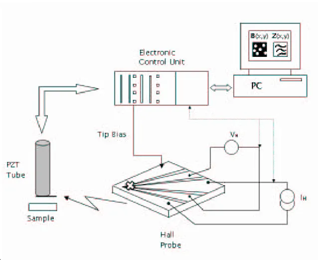
..
Figure 2.2: Schematic description of the Scanning Hall Probe Microscope In SHPM a submicrometer Hall probe is scanned over the sample surface to measure the perpendicular component of the surface magnetic fields using conventional scanning tunnelling microscopy (STM) positioning techniques.
CHAPTER 2. SCANNING HALL PROBE MICROSCOPE 13
2.2.1
The Microscope Body
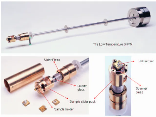
The probe, course positioning and piezoelectric scanner systems are combined into the microscope body as shown in Fig.2.3
The probe is the most critical component of a scanning probe microscope; because it determines the interaction level to the sample and the ultimate res-olution of the system. Different probes can measure different properties of the sample. The desirable properties for a probe depend on the imaging mode and the application. In SHPM, the sensor is the Hall probe; a micro fabricated mag-netometer. The production sequence and specifications of the Hall sensors used in the experiments is given in section 3. The microscope uses a piezoelectric tube
..
Figure 2.3: The LT-SHPM
(PZT) for course positioning the sample with respect to the probe in a stick-slip approach mechanism in three dimensions. The movement of the probe over the
CHAPTER 2. SCANNING HALL PROBE MICROSCOPE 14
sample, namely the scan is also done with another piezoelectric tube. Piezo-electric materials are ceramics that change dimensions in response to an applied electric field. Conversely, they develop an electrical potential in response to me-chanical pressure. Piezoelectric tube scanners are the critical elements, giving sub-angstrom resolution, at high speeds in a compact design.
Course positioning is done with the movement of the sample puck that holds the specimen. The design is based on a stick-slip approach mechanism. The sample holder is tightened to a quartz tube using a leaf spring. The end of the tube is attached to the slider PZT. The voltage pulses sent to PZT creates a mechanical movement and puck moves towards the probe.
Another piezoelectric crystal tube is used for fine approach and scanning over the sample surface. Electrodes are attached to the outside of the tube, segmenting it electrically into vertical quadrants, for +x, +y, -x, and -y travel (Fig.2.4). In addition, z voltage is also added to these electrodes to provide the vertical motion. Actually, any kind of motion is possible in 3 dimension by properly arranging the voltage to the quadrants.
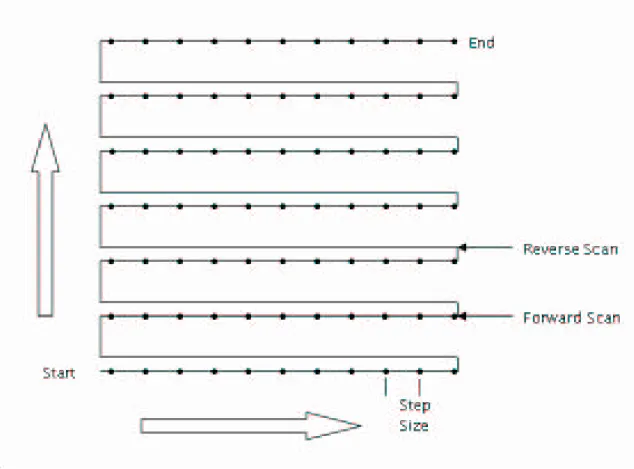
Scan is done by changing the voltage applied to the +x, +y, -x, and -y elec-trodes. The scanned area is swept by a pattern similar to a matrix or an array (Fig.2.5). The scanner moves across the first line of the scan, and back. It then steps in the perpendicular direction to the second scan line, moves across it and back, then to the third line, and so forth. While the scanner is moving across a scan line, the image data are gathered digitally at equally spaced intervals. The spacing between the data points is called the step size. The step size is deter-mined by the full scan size and the number of data points per line which gives the resolution. For example, if a 20×20 µm2 area is scanned with 128 pixel
resolu-tion means that the microscope will divide the 20 µm into 128 pieces along both vertical and horizontal direction, and a 128×128 matrix will be scanned with a step size of ∼ 0.16 µm.
The maximum scan size that can be achieved with a particular piezoelectric scanner, depends upon the length of the scanner tube, the diameter of the tube, its wall thickness, and the strain coefficients of the particular ceramic material
CHAPTER 2. SCANNING HALL PROBE MICROSCOPE 15
..
CHAPTER 2. SCANNING HALL PROBE MICROSCOPE 16
..
Figure 2.5: Description of scan method of the scanner tube
from which it is fabricated. Our LT-SHPM scanner has a 50 µm × 50 µm scan range in xy and 4.8 µm in z direction at 300 K. These drop by a factor of ∼ 3.8 at 77 K.
2.2.2
The Electronics and Computer Control Unit
Since the probe has to come to a very close proximity of the surface, the approach and the scan process must be done in a controlled fashion. Because, there exist possibility of crashing the sensor on to the sample, which eventually can damage either sample, probe or both . All the units on the body of the microscope are controlled via a computer program and an the electronics control unit.
CHAPTER 2. SCANNING HALL PROBE MICROSCOPE 17
..
Figure 2.6: The electronic control unit
The electronics has the ability to control any kind of motion of the piezo-electric tubes, the sample-probe interaction and data gathering. The microscope uses an STM tip fabricated on the sensor which detects the tunnelling current between the sample and the probe by means of applied bias voltage to the sample. The tunnelling current is a strong function of the distance, so controlling of the tunnelling current means controlling of the distance between the sample and Hall sensor. A feedback loop maintains a constant tunnelling current between tip and sample. If the desired current is not detected course approach mechanism makes a forward step and the fine approach mechanism lengthens the scan PZT which moves the probe towards sample, until the indicated current value is achieved. The electronics prevents the probe from crushing to the surface. If the fixed tunnelling current is exceeded, the Hall sensor is immediately retracted.
The electronics also facilitates the computer interface with the help of a digital I/O card at the computer.
Incoming data are converted into a visible picture of the magnetic profile with the software. The raw two dimensional picture is stored in either bitmap or ASCII format. The interactive data language used by the software makes it possible to obtain 3D visualization and animation. Sometimes further filtering and processing are needed to decrease the unwanted noise effects. For example, low pass, high pass, bandpass, and median filtering may be needed for reduction
CHAPTER 2. SCANNING HALL PROBE MICROSCOPE 18
of the noise. Another correction may be needed to correct the hysteresis or other effect of the scanner piezoelectric tube. Sometimes it is also necessary to change the appearance of the image, like its color or dimensions. All of these are done by the software.
The software also gives ability to define any control parameters such as sample bias voltage, Hall current, tunnelling current, loop gain, amplifier gain and band-width, position of PZT and so on. Any kind of measurement on the processed images like, histogram, crossection, averaging are also possible.
2.2.3
The LT-SHPM Specifications
The PZT have scan range area in xy plane up to 50×50 µm2 and extension
of 4.8 µm in z direction at 300K. At 77K, these values decrease by a factor of 3.8 approximately.
Any current value up to ±1 mA can be applied to the Hall sensor with 16 bit resolution. The HP post amplifier gain can be set to 1,10,100 or 1000; and possible bandwidth values are 0.1, 1, 10, 100 kHz. Image resolution can be set between 32 to 1024 pixels.
The microscope can operate at three different modes for data acquisition, (a)The Simultaneous STM/SHPM Mode: In this mode both the Hall bar signal and STM tip topography is monitored and displayed. Thus sur-face topography obtained by STM feedback together with the corresponding magnetic profile obtained by HP. This mode is rather slow.
(b) The Fast SHPM Mode: In this mode, only the Hall Probe (HP) junction output is monitored and displayed during the measurement, line by line,
(c) The Real Time SHPM Mode: In this mode the entire measurement is finished and than the magnetic images are displayed. This mode gives the ability of LT-SHPM measurements with speeds up to ∼1 frame per second.
CHAPTER 2. SCANNING HALL PROBE MICROSCOPE 19
The last two modes can only be run while the HP is lifted off from the sample a safe distance.
Chapter 3
Hall Sensor Fabrication
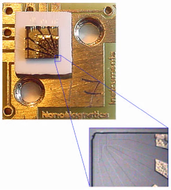
Micro-photofabrication of Hall sensors consists of a logical sequence of lithogra-phy, etch and deposition steps carried out in a Class 100 clean room environment. Since the Hall sensor is the most important part of the microscope that gathers the data, extreme care must be given during its production to get a good sensor. In this chapter, the production steps are explained and supported by pictures that are taken during the production.
3.1
Wafer Preparation for Microfabrication
Although in industry production of micro chips are done using the whole wafer mostly, the cost prohibits us to do so. Instead, the wafers are scribed to have 5x5 millimeter sized square pieces that are capable of giving 4 sensors each.
3.1.1
Wafer Rounding
Scribed wafers are actually ready for production after they have cleaned. But a well known problem, accumulation of photo resist at the edge and corners during
CHAPTER 3. HALL SENSOR FABRICATION 21
spinning; so called edge beads, prevents the mask to get in physical contact across the wafer and some unwanted diffraction of light during the exposure destroys the pattern or lowers the quality of the desired shape. If the whole wafer is used, its rounded edges can solve the problem. However, in our case, the used pieces are just small squares scribed out of the whole wafer. The solution is rounding the edges and corners of the wafers. This is possible with some combination of photolithography and wet chemical etch. A 4x4 millimeter sized square mask is used to obtain a 0.5 mm photoresist free area around the edges and the chip is sunk in to a HCl solution (H2O:H2O2:HCl, 4:10:55) upside down; after the back
side of it coated by resist in order to prevent it from being etched from back, for an hour, which eventually rounds the edges and corners.
..
CHAPTER 3. HALL SENSOR FABRICATION 22
3.1.2
Sample Cleaning
The standard sample cleaning method we used is known as the three solvent cleaning, which has the following steps:
(1) boiling in trichlorethane (TCA) for 2 min., (2) dipping in Acetone for 5 min.,
(3) boiling in Isopropilalcohol (IPA) for 3 min.,
(4) cleaning with de-ionized water and blow drying with nitrogen.
But, if the wafers are not much dirty dipping in acetone followed by dipping in IPA is usually sufficient. Cleaning is repeated at the beginning of each lithographic process.
3.2
Hall Probe Etch
The most crucial step in microfabrication is Hall probe etch, in which the Hall sensor is defined. The lithography is critical due to the Hall bar, which is 1 micro meter in size close to the resolution limits of our Karl S¨uss MJB3 mask aligner. The pattern is transferred by exposed UV light on to the photoresist layer that was spun, and developed which is then defined by etching in H2O:H2O2:H2SO4
(320:8:1) solution. The typical etch rate is 2 nm/s at 210 C. The affectivity of
lithography, in other words, how good your Hall bars’ shape is, depends on litho-graphic criteria such as spin rate and time, expose power and development time, etc. The resist thickness must not exceed the critical dimension of the transferred pattern to increase the resolution, since as the thickness increases the effect of diffraction and resultant defect rate also increase. To achieve 1 µm thickness, AZ5214E photoresist is spun at 10000 rpm/min for 40 sec. Before exposure, chips are hot baked at 1100 C for 55 seconds at the beginning of each lithography
pro-cedure to evaporate the resist solvent and to harden the photoresist, in order to prevent sticking to the mask.
CHAPTER 3. HALL SENSOR FABRICATION 23
The wafers are etched down for a required depth and the probes are defined. The active 2DEG layer of GaAs wafers lie 80 nm. beneath the surface and for Hall Bar definition 50-60 nm etch is usually sufficient which is well enough to not destroy the energy band of the 2DEG layer. For InSb wafers, this etch is not that critical, one must etch the wafer down until the the thickness of InSb layer exceeded, since the substrate is undoped semi-insulating GaAs.
Etching process can be done with wet chemical etch using acid solutions or with dry etch using plasma produced by various gases (Reactive Ion Etching, RIE). In wet etch, chips are hot baked for 2 minutes at 1200 C to prevent the
resist form being etched by the acid solution after the development of the exposed resist. In dry etch however, ions in the plasma can easily damage the photoresist, so depending on the gas used a metal; like Aluminium, may be necessary to protect the sample.
3.3
Mesa Etch
To separate the 4 individual Hall probes on a chip and to obtain a mesa corner that serves as a STM tip, 100 µm wide cross-hair like area is defined between the probes and etched down approximately 1-1.2 µm with H2O:H2O2:H2SO4 (40:8:1)
solution, which has a typical etch rate of 13 nm/s. This area is used to scribe and cleave the probes from each other after the microfabrication finishes.
3.4
Recess Etch
While performing an experiment the sensor comes to a close proximity of the sample which is as close as 2500-3000 ˙A. Thus, if there exists any part of the chip higher than the Hall Bar, it is impossible to control the tunnelling which is a sign for being close enough to the sample for scan. Also, these parts may touch to the sample and harm the sample physically. Hence, to prevent the bonding wires to exceed the sensor surface, an area around the edges of the chip defined is etched
CHAPTER 3. HALL SENSOR FABRICATION 24
down for 50-60 µm for wire bonding.
3.5
Ohmic Contact Metallization
The generated Hall voltage by the sensor should be sent to the Hall amplifier with a minimum possible series resistance to have the lowest noise. Since the 2DEG material is a semiconductor, it is not a good electrical conductor, a metallic layer must be diffused into the region to lower the noise. To achieve this, the area to be coated is defined by optical lithography and the samples are soaked into Chlorobenzene before they are developed, for 15 minutes to get undercut and easy lift off. Germanium, gold and nickel are evaporated on the sample through the mask in a box coater with a base pressure of, 10−7 mbar. Acetone is used
for lift off and coated metals are diffused by annealing the wafer at 450oC for 45
seconds with Rapid Thermal Process (RTP) system.
Another metallization is done to the same area after RTP whose content is Ti and Au with the thickness of 10 nm and 150 nm respectively. Titanium is used to stick the gold to the surface. This metallization completes the ohmic metallization and provides a layer for easier bond wiring.
For InSb and Bi wafers there is no need for the first step and annealing, just the second metallization is enough.
3.6
Tip Metallization
The sensor is guided with an STM tip which brings the sensor to a close proximity of the sample in a controlled fashion. The tip is the gold coated mesa corner, which is ∼13 µm away from the Hall cross. The tip is defined by lithog-raphy and the chip soaked into Chlorobenzene and then developed. Ti and Au are evaporated and lift-off is performed in acetone.
CHAPTER 3. HALL SENSOR FABRICATION 25
3.7
Cleaving and Sensor mounting
Finished chips are cleaved into 4 sensor units. Then, these sensors are mounted on a chip holder; a PCB holder, which makes it possible to attach the sensor on the microscope. The holder and the sensor are wired to each other with gold wires of diameter 12 µm.
..
CHAPTER 3. HALL SENSOR FABRICATION 26
3.8
Characterization and Noise Measurement
The electronic properties of semiconductors can be varied during their pro-duction by changing the dopant type or concentration. Also, the environmental conditions, like, temperature, light, etc. are effective on the carrier density, mo-bility and hence, resistivity. Therefore, the most ideal material must be chosen in Hall sensor microfabrication to improve the field sensitivity and spatial resolution for the desired application.
The shape and the thickness are also effective on the ultimate resolution. The thinner and narrower the Hall bar, the higher the spatial resolution becomes. Typically higher spatial resolution is achieved by symmetrically scaling the volt-age and current leads, however there are some numerical studies related to the probe geometry [14], that shows if one of the voltage strip is narrowed assuming the diffusive transport conditions, the spatial resolution will increase.
Another factor that determines the ultimate resolution is how good Hall volt-age VH across the sensor is measured. This quantity contains a combination of
the noise sources due to electronics and the noise coming from the intrinsic prop-erties of the probe itself that is, the voltage noise of the amplifier and the noise due to the series resistance of the Hall sensor (Rs), as well as the excess noise
from the sensor.
The Hall voltage measured at the output of the low noise amplifier is, a func-tion of applied Hall current (IH), the Hall coefficient (RH), gain of the amplifier
(G), and the magnetic field (B) perpendicular to the sensor,
VH = RH × IH × B × G (3.1)
Rearranging this equation, we get the dependence of the minimum detectable magnetic field on these parameters.
Bmin =
Vnoise
RH × IH × G
CHAPTER 3. HALL SENSOR FABRICATION 27
where Vnoise is the noise measured at the output of the amplifier. The above
equation leads a conclusion that, it is desirable to drive the Hall probe with the highest permissible current. But the Hall current cannot be increased indefinitely and there is a maximum useable current I(Hall)max. Because, as the current is
increased, the voltage noise of series resistance Rs increases due to heating of
the charge carriers and the lattice. The current increases the kinetic energy of the electrons, heating them hence increasing the noise. As the number of free charge carriers increase the Hall coefficient decreases. Therefore, the minimum detectable magnetic field increases.
The main noise component up to a certain bias current level Imax is the
John-son noise of the series resistance of the Hall bar [12].
Vn=
q
4kBT Rsf (3.3)
where f, kB, T, Rs are the measurement bandwidth, Boltzman constant,
teper-ature and series resistance, respectively. For the case where the Hall current is less than Imax, the signal to noise (SNR) ratio can be defined as:
SN R = √IHallRHB 4kBT Rsf
(3.4) However, when this current level is exceeded, the noise start to increase with the Hall current.
The voltage noise level can be analyzed using fast Fourier transform (FFT) signal analyzer, which is inexpensively implemented in the software. The noise spectra of the micro-Hall sensors are measured at different Hall currents to find optimum operating conditions and I(Hall)max. During the procedure, the gain and
bandwidth of the Hall amplifier were set to 10010 and 1kHz, respectively. The noise spectra were measured using a FFT signal analyzer in a 1Hz equivalent bandwidth at different Hall currents.
CHAPTER 3. HALL SENSOR FABRICATION 28
..
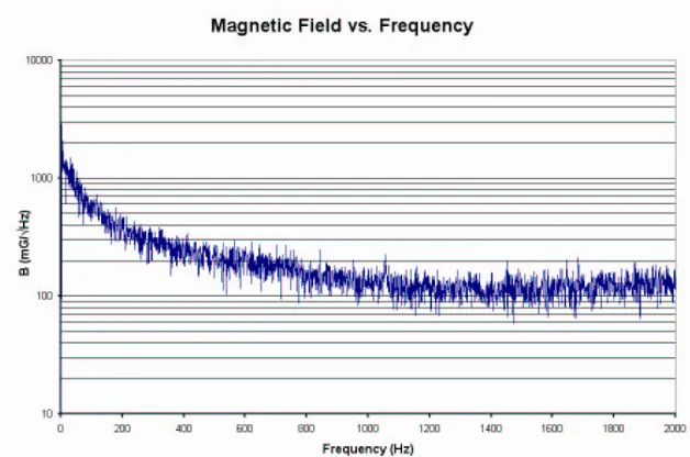
Figure 3.3: Noise spectrum of the GaAs Hall probe for 2.5 µA current at 300 K.
3.8.1
Gallium Arsenide (GaAs) Hall Sensors
These probes are fabricated using molecular beam epitaxially grown GaAs/AlGaAs heterostructure providing 2 dimensional electron gas (2DEG) sup-plied by Dr. Hadas Shtrikman of Weizmann Institute of Science. The active 2DEG layer is 80 nm beneath the surface. The Hall bar is placed ∼13 µm away from the mesa corner. The bars are 1 µm in size. However, they give ∼0.85 µm electrical width due to edge depletion. It has a typical series resistance of 50-60 kΩ at 300 K, which decreases to 4-5 kΩ at 77 K. The typical Hall coefficient RH
is 0.3 Ω/G at 77 K. Specifications of GaAs sensors are given in table 3.1
Figure 3.3 shows a typical magnetic field noise spectrum of the Hall probe for 2.5 µA applied current at 300 K. The high level of noise at the lower fre-quencies is due to 1/f noise. This spectrum can be analyzed further for some specific frequency and corresponding current values which give the minimum de-tectable magnetic field as a function of the applied current as shown in Fig. 3.4.
CHAPTER 3. HALL SENSOR FABRICATION 29
..
Figure 3.4: The minimum detectable magnetic field as a function of Hall current at 300 K for GaAs Hall probe
This figure shows that the minimum detectable field changes from 1000 to 100 mG/√Hz (100-10 µT/√Hz) depending on the Hall current. Thus the increase in Hall current also decreases the minimum detectable magnetic field unless the maximum current is not exceeded.
The value of the minimum detectable magnetic field is rather high at room temperature. However, at 77 K the noise level decreases and the minimum de-tectable magnetic field decreases by an order of magnitude, which can be seen in Fig. 3.5. This is due to increase in mobility µ, while the carrier concentration stays more or less constant. The minimum detectable field is 1.8-2 mG/√Hz at 77K in this case. The corresponding minimum detectable voltage graph is given in Fig. 3.6. It can be seen from these two figures that Imax is around 25 µA. Both
voltage noise and magnetic field noise behave similarly and start to increase after that point.
The similar 1/f noise can also be seen from voltage noise spectra. The spectra measured at 10 and 20 µA are shown in Fig. 3.7 and 3.8, respectively. It is seen
CHAPTER 3. HALL SENSOR FABRICATION 30
..
Figure 3.5: The minimum detectable magnetic field as a function of Hall current at 77 K for GaAs Hall probe.
..
Figure 3.6: Voltage noise as a function of Hall current at 77 K for GaAs Hall probe.
CHAPTER 3. HALL SENSOR FABRICATION 31
..
Figure 3.7: The voltage noise spectrum of GaAs Hall probe at 77 K for IHall=10
µA.
..
Figure 3.8: The voltage noise spectrum of GaAs Hall probe at 77 K for IHall=20
CHAPTER 3. HALL SENSOR FABRICATION 32
that as the current increases, so does the voltage noise.
3.8.2
Indium Antimonide (InSb) Thin Film Hall Sensors
Indium antimonide is a good candidate to lower the noise level of the Hall probes due to their high mobility at 300 K. The InSb wafer used in Hall probe microfabrication has 1 µm InSb thin film grown on undoped GaAs substrate. The sheet density ns and the mobility µ are 2×1012 cm−2 and 55,500 cm2Vs,
respec-tively. Corresponding Hall coefficient, RH is 0.034 Ω/G. Their series resistance
has a typical value of 2-3 kΩ at 300 K which is comparable to the GaAs at 77K. Table 3.2 summarizes the characteristics of InSb sensors.
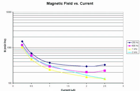
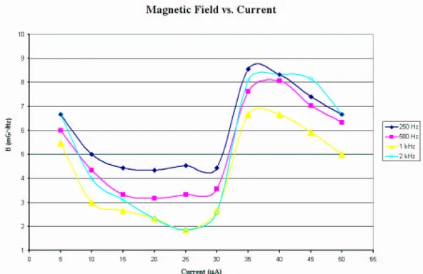
Fig. 3.9 and 3.10 show magnetic field and voltage noise plotted as a function of Hall current at four different measurement frequencies: 250, 500, 1000 and 2000 Hz, respectively. The graphs in Fig. 3.9 and 3.10 belong to a Hall probe with 1 µm sized Hall bar. Similar graphs are shown for a Hall probe whose bar is 12 µm in size, in Fig. 3.11 and 3.12.
The minimum detectable magnetic field can be estimated from the Fig. 3.9 to be 6-10mG/√Hz at IHall= 50 µA for 1 µm Hall sensor. It is possible to drive
much more current from the 12 µm sized Hall sensor. This gives a much better noise level, 0.5 mG/√Hz at IHall= 1000 µA at 1 kHz!
InSb thin-film Hall probes were used to image magnetic domain structures of crystalline garnet films [15]. The sample is vacuum coated with a 20-nm layer of gold film to enable SHPM imaging. Bi-substituted iron garnet films were measured using Hall currents of 3, 30, and 50 A, respectively. The images are acquired in the liftoff mode with the InSb micro-Hall sensor at a height of 0.35 µm. The black and white regions given in Fig. 3.13 correspond to surface field fluctuations into and out of the plane of the paper ranging between ±52 G.
CHAPTER 3. HALL SENSOR FABRICATION 33
..
Figure 3.9: The minimum detectable magnetic field as a function of current at 300 K with InSb Hall sensor (Hall bar size=1 µm).
..
Figure 3.10: The minimum detectable voltage as a function of current at 300 K with InSb Hall sensor (Hall bar size=1 µm).
CHAPTER 3. HALL SENSOR FABRICATION 34
..
Figure 3.11: The minimum detectable magnetic field as a function of current at 300 K with InSb Hall sensor (Hall bar size=12 µm).
..
Figure 3.12: The minimum detectable voltage as a function of current at 300 K with InSb Hall sensor (Hall bar size=12 µm).
CHAPTER 3. HALL SENSOR FABRICATION 35
..
Figure 3.13: 25 µm × 25 µm RT-SHPM images of 5.5 µm thick crystalline bismuth-substituted iron garnet films obtained with Hall currents of (a) 3, (b) 30, and (c) 50 µA [15].
3.8.3
Other Materials
GaAs and InSb are not the only choice for the Hall probes to be used in SHPM. Strained Gallium Indium Arsenide (GaInAs) is also a good alternative to InSb for the production of the probes that will serve at room temperature. Also, bismuth (Bi) sensors are being used especially, if the spatial resolution is important. The surface charge depletion effect which prevents the fabrication of Hall bar with sizes smaller than 0.5 µm using GaAs, is not a problem in Bi sensors. As small as 120 nm-sized Hall probes have been reported [16,17].
CHAPTER 3. HALL SENSOR FABRICATION 36
Table 3.1: The specifications of GaAs Hall sensors at 77K
Carrier Density (ns): 6×1011 cm−2
Mobility (µ): 49000 cm2/Vs
Hall Coefficient (RH): 0.3 Ω/G
Series Resistance Rs : 3.5-4 kΩ
Table 3.2: The specifications of InSb Hall sensors at 300K
Film Thickness: 1 µm
Carrier Density (ns): 2×1012 cm−2
Mobility (µ): 55500 cm2/Vs
Hall Coefficient (RH): 0.03 Ω/G
Chapter 4
Results
The high temperature superconductors represent a new class of materials which bear extraordinary superconducting and magnetic properties and great potential for wide-ranging technological applications.
In the experiments two different type of high temperature superconduc-tors namely, a Ag-sheathed Bi-2223 tape and a single crystal Bi2Sr2CaCu2O8+δ
(BSCCO) superconductors are used.
BSCCO exhibits poor flux pinning ; i.e., less resistance to the motion of magnetic flux. This phenomenon where a magnet’s lines of force called flux become trapped or pinned inside a superconducting material, usually because of the grain boundaries or impurities, is called the flux pinning. The tapes are therefore treated by various methods to increase pinning, hence increasing the criticial current density, Jc.
4.1
Preparation for Scan
The samples are cleaned and placed on the sample holder. The sample and the Hall probe brought together co-linearly at the end of the microscope body. The sample is tilted by 1-1.5o with respect to the Hall probe. This is necessary
CHAPTER 4. RESULTS 38
..
Figure 4.1: Experimental setup
to bring the corner of the mesa, that serves as a STM tip, into the closest point to the sample.
The microscope is placed in to a single stainless steel cryostat tube which is flushed with helium gas several times. Helium serves as heat exchange gas between the SHPM and the steel body of the cryostat. The microscope in the cryostat is than cooled down to 77 K at a rate of ∼2-3 K/s and placed in to a liquid nitrogen dewar to keep the temperature constant at 77 K. The dewar is placed on a vibration isolation stage to get rid of the vibration of the floor. The external magnetic field is applied by a coil wound around the cryostat body. This coil can supply magnetic fields up to ±140 Oe with ±10 V.
CHAPTER 4. RESULTS 39
4.2
Ag-Sheathed Bi-2223 BSCCO Tape
(Bi,Pb)2Sr2Ca2Cu3Ox (Bi-2223), the leading high temperature superconductor
with Tc of 108 K, has been demonstrated to be the most technically viable present
materials for superconducting application to electric power transmission lines, fault current limiters, transformers, electromagnets and motors[18]. Moreover, silver sheathed Bi-2223 is the only high Tc superconducting material that can be
fabricated in long lengths suitable for large-scale engineering applications.
..
CHAPTER 4. RESULTS 40
The BSCCO tape is provided by Prof. D. Larbalestier’s group from Univer-sity of Wisconsin-Madison. The tape is prepared with powder in tube (PIT) technique. This technique involves the following steps of production; precursor oxide powder is packed into a silver billet. The billet is drown to a fine wire and wire is rolled to a flat ribbon. This ribbon is treated with heat to produce nearly phase pure Bi-2223. Grain microstructure is conducive to the flow of supercur-rent through the composite wire. Critical cursupercur-rent, Jc, is strongly determined by
the grain boundary misorientations [19]. The tape mounted on a carbon mount and polished with 0.05 µm Al2O3 powder in methanol so as to achieve the best
possible flat surface [18]. Finally, the sample is gold coated with 10 nm thickness. The silver and BSCCO boundary is clearly seen in Fig. 4.2 which shows the tape and the possible scanned region.
Several scans are performed under different conditions using a 1 µm sized Hall probe micro fabricated on GaAs/AlGaAs hetereo structure with 2DEG. The specifications of the Hall probe are given in sec.3.8.1.
First scan is done after applying an external magnetic field that is varied between ± 138 Oe and back to zero in a B-H curve measurement. Fig. 4.3 shows the SHPM image and the cross section taken diagonally. The blue region belongs to silver shield, green and red regions belong to BSCCO. The cross-section in the same figure shows that, as going from metallic region through the superconductor, the trapped flux due to externally applied magnetic field increases as expected. The cross-section is in a good agreement with the magneto optical measurements[20] done on the tape as shown in Fig.4.5.
Then, the external magnetic field is ramped to + 138 Oe and brought back to zero. Fig. 4.4 shows the SHPM image and the cross section along the diagonal.
Further investigation is possible by measuring the B-H curves or the hys-teresis loop. A closed curve obtained for a material by plotting corresponding values of magnetic induction, B, against magnetizing force, H, is called the B-H curve. Hysteresis, as it applies to a superconductor, relates to the dynamic re-sponse of a superconductor to a strong magnetic field impinged upon it. As the strength of magnetic field (H) increases, the flux penetrates into superconductor
CHAPTER 4. RESULTS 41
..
Figure 4.3: The SHPM image and cross section taken after externally applied varying ± 138 Oe external magnetic field and back to zero.
..
Figure 4.4: The SHPM image and cross section taken after externally applied varying, only + 138 Oe external magnetic field and back to zero.
CHAPTER 4. RESULTS 42
in the form of quantized vortices and the critical transition temperature (Tc) of
a superconductor will decrease. If we carry on increasing the external magnetic field, at some point superconductivity will completely disappear. However, as the magnetic field is gradually withdrawn, the vortices (quantized flux lines) can not get out completely. Herein lies the hysteresis and it is one of the direct evidence of superconductivity.
BH curves measured starting from the silver region, towards the supercon-ducting region along the diagonal (Fig 4.6). As a result, an increase in the hysteresis is obtained similar to the diagonal crossection.(Fig.4.7-Fig.4.17)
..
CHAPTER 4. RESULTS 43
..
Figure 4.6: BH curves taken diagonally.
..
CHAPTER 4. RESULTS 44
..
Figure 4.8: The BH curve at the point B.
..
CHAPTER 4. RESULTS 45
..
Figure 4.10: The BH curve at the point D.
..
CHAPTER 4. RESULTS 46
..
Figure 4.12: The BH curve at the point F.
..
CHAPTER 4. RESULTS 47
..
Figure 4.14: The BH curve at the point H.
..
CHAPTER 4. RESULTS 48
..
Figure 4.16: The BH curve at the point J.
..
CHAPTER 4. RESULTS 49
Another scan is done after the system is heated to 130 K which is above the critical temperature and cooled down to 77 K again. Before the system is cooled down again, the LT-SHPM system and the cryostat are degaussed with oscillatory decaying external magnetic field Hext to minimize the remanent field
of the system. The integration of total flux from the SHPM image implies that there is still some remanent field in the system, Br=0.73 Gauss and estimated
number of vortices within the image is 6. The acquired image is shown in Fig. 4.18 and the scan parameters are given in Table 4.2. The number of vortices in the scanned area is estimated using the histogram function and following formula:
N umber of vortices = Baverage× Area Φ0
(4.1) Φ0 = 20.7 Gµm2 (4.2)
..
Figure 4.18: SHPM image of overlapped vortices, the figure histogram of the image and the crossections.
CHAPTER 4. RESULTS 50
Table 4.1: The scan parameters of the SHPM image shown in Fig.4.3 and 4.4
Scan Size: 13µm × 13µm Resolution: 256 pixels Scan Speed: 10 µm/sec. Scan Mode: Fast SHPM Scan Hall Current: 10 µA
Image Gain: 8 Voltage Gain:10010 Bandwidth:1 kHz No.of averages:10
Table 4.2: The scan parameters of the SHPM image shown in Fig.4.18
Scan Size: 13µm × 13µm Resolution: 256 pixels Scan Speed: 10 µm/sec. Scan Mode: Fast SHPM Scan Hall Current: 10 µA
Image Gain: 8 Voltage Gain:10010 Bandwidth:0.1 kHz No.of averages:25
4.3
Single Crystal BSCCO-2212
The single crystal BSCCO-2212 we have used for our investigations is provided by Prof. Kazuo Kadowaki of Tsukuba University. The sample is prepared for the experiment without gold coating, similar to the previous one and the same probe is used for scan. The system is degaussed and zero field cooled to 77 K. The sample has a critical temperature Tc=85 K.
The LT-SHPM images with 256 pixel resolution and scan size of 13µm × 13µm are obtained with single vortex resolution. The scan performed with fast scan mode having a scan speed of 10 µm/s. Figure 4.19 shows individual vortices
CHAPTER 4. RESULTS 51
pinned at various sites, probably at the oxygen deficient regions. The trapped flux lie in stripes parallel to one of the crystallographic axes, separated by regions free from strong pinning sites [21]. This chain like behavior can be seen in Fig.4.20.
The vertical height of the image in Fig. 4.21 is about 1.8 Gauss. The 3D appearance of the same image can be seen in Fig. 4.22.
Vortices melt at some well defined field and temperature depended phase boundary [22]. Static local magnetic induction measurements were performed at 77 K applying a varying external magnetic field of an amplitude of ±138 Oe. Jumps in the local magnetic induction curve around 100 Oe are the lattice melting transitions [23-25]. This behavior can be seen in Fig.4.24. This melting field is consistent with the values given by Prof. Kadowaki.
Moreover, the creation of the vortices were observed varying the applied field. Starting with the zero field, the magnitude of the external field is decreased to -4 Oe gradually. The negative field has penetrated and anti-vortices were created. Thus it is possible to observe that changes using Real Time SHPM scan mode (∼ 1 frame/s). We observed that the vortices are not pinned but instead they are in motion along the deficiency sites. Figure 4.25 shows a few of these anti-vortices. Similarly, another real time imaging performed in which we have started with zero field and applied +6 Oe gradually increasing the field. As the field value increased vortices created along the pinning sites. Then the applied field is decreased until -6 Oe achieved. Previous vortices are annihilated by negative magnetic field and anti-vortices penetrated in to superconductor.(Fig. 4.26)
CHAPTER 4. RESULTS 52
..
Figure 4.19: LT-SHPM image of individual vortices with single quantum flux resolution at 77 K
Table 4.3: The scan parameters of the LT-SHPM image shown in Fig.4.19
Scan Size: 13µm × 13µm Resolution: 256 pixels Scan Speed: 10 µm/sec. Scan Mode: Fast SHPM Scan Hall Current: -20 µA
Image Gain: 8 Voltage Gain:10010 Bandwidth:1 kHz No.of averages:100
CHAPTER 4. RESULTS 53
..
Figure 4.20: LT-SHPM image of chain like alignment of vortices at 77K Table 4.4: The scan parameters of the LT-SHPM image shown in Fig.4.20
Scan Size: 13µm × 13µm Resolution: 256 pixels Scan Speed: 10 µm/sec. Scan Mode: Fast SHPM Scan Hall Current: -20 µA
Image Gain: 8 Voltage Gain:10010 Bandwidth:1 kHz No.of averages:10
CHAPTER 4. RESULTS 54
..
CHAPTER 4. RESULTS 55
..
CHAPTER 4. RESULTS 56
..
Figure 4.23: BH curve measured at 77K
..
CHAPTER 4. RESULTS 57
..
Figure 4.25: LT-SHPM real time images of anti-vortex penetrating into BSCCO-2212 single crystal at 77 K.
CHAPTER 4. RESULTS 58
..
Figure 4.26: LT-SHPM real time images of vortex penetrating into BSCCO-2212 single crystal at 77 K.
Chapter 5
Conclusions and Future Work
In conclusion, a low temperature scanning Hall probe microscope (LT-SHPM) is used to investigate the magnetization properties of vortex structures, vortex pinning and vortex lattice melting of BSCCO type high Tc superconductors.
The LT-SHPM imaging is performed using Hall probes manufactured on GaAs/AlGaAs 2DEG heterostructure. The probes are micro fabricated in Bilkent Class 100 facility with the spatial resolution of ∼0.85 µm and field resolution of 1.5 mG/√Hz. during the microfabrication, to achieve better lithographic res-olution getting rid of edge beads, wafers are rounded. In addition, InSb Hall probes are also microfabricated using the similar methods and are used to image the 5.5 µm thick crystalline bismuth substituted iron garnet films at 300 M. All the microfabricated Hall sensors are characterized using a FFT signal analyzer. Their minimum magnetic field detection level, optimal operation current values and Hall coefficients are obtained.
The inductance under magnetic field of Ag-Sheathed Bi-2223 BSCCO tape is investigated and the results are compared to the previous magneto optical studies. It is found that the magnetisation properties of the Ag-BSCCO boundary are in a good agrement with the magneto optical images which was clear in diagonally taken crossections.
CHAPTER 5. CONCLUSIONS AND FUTURE WORK 60
The creation and annihilation of the vortices under variable magnetic field and the pinning is observed with single quantum flux resolution using a high quality BSCCO-2212 singe crystal. The vortices pinned at various sites, probably at the oxygen deficient regions. It is observed that the trapped flux lie in stripes parallel to one of the crystallographic axes, separated by regions free from strong pinning sites. In addition, static local magnetic induction measurements were performed at 07K applying a varying external magnetic field of an amplitude of ±138 Oe. These measurements showed melting transitions of the vortices around 100 Oe. Moreover real time images of anti-vortex creations in BSCCO were imaged.
All the images are averaged as much as possible to decrease the 1/f noise to get the cleanest images.
The main aim for any future work is to improve the microscope by producing better probes and lowering the electronics noise. Moreover, increasing the oper-ational flexibility of the microscope ,such as making it possible to work for non conducting materials, have importance. As we improve the microscope, investi-gation of more challenging properties of magnetic materials and superconductors will be easier.
Bibliography
[1] R. Wiesendanger, Scanning Probe Microscopy and Spectroscopy; Method and Applications , Cambridge University Press, 1994.
[2] R. Wiesendanger, Nano-scale studies of quantum phenomena by scanning probe spectroscopy, VACUUM, 65(2), 235-236, 2002.
[3] A. M. Chang, H. D. Hallen, L. Harriot, H. F. Hess, H. L. Kao, R. E. Miller, R. Wolfe, and J. van der Ziel, Scanning Hall Probe Microscopy Appl. Phys. Lett.,61(16), 1974-1976, 1992.
[4] A. Oral, S. Bending, M. Heini, Scanning Hall probe microscopy of supercon-ductors and magnetic materials, J. Vac. Sci. Technol. B, 14(2), 1202-1205, 1996.
[5] T. Fukumura, H. Sugawara, K. Kitazawa, T. Hasegawa, Y. Nagamune, T. Noda, H. Sakaki, Development of scanning Hall probe microscope for simul-taneous magnetic and topografic imaging, Micron, 30, 575-578, 1999.
[6] L. N. Vu, D. J. van Harlingen design and implementation of a scanning SQUID microscope, IEEE Trans. Appl. Supercond., 3, 1918-1921, 1993. [7] J. R. Kirtley, M. B. Ketchen, K. G. Stawiasz, J. Z. Sun, W. J. Gallagher, S.
H. Blanton, S. J. Wind, High resolution scanning SQUID microscope, Appl. Phys. Lett., 60, 1138-1140, 1995.
[8] Y. Martin, H. K. Wickramasinghe, Magnetic imaging by force microscopy with 100 ˙A resolution, Appl. Phys. Lett., 50, 1455-1457, 1987.
BIBLIOGRAPHY 62
[9] Y. Martin, D. Ruger, H. K. Wickramasinghe, High resolution magnetic imag-ing of domains in TbFe by force microscopy, Appl. Phys. Lett., 52, 244-246, 1988.
[10] J. M. Florczak, E. D. Dahlberg, Detecting two magnetization components by the magneto-optical Kerr effect, J. Appl. Phys., 67(12), 7520-7525, 1990. [11] G. C. Rauch, R. F. Krause, C. P. Izzo, K. Foster, W. O. Barlett, J. Appl.
Phys., 55, 2145, 1984.
[12] Y. Matsuda, A. Fukuhara, T. Yoshioka, S. Hasegawa, A. Tonomura and Q. Ru, Computer reconstruction from electron holograms and observation of fluxon dynamics, Phys. Rev. Lett., 66, 457, 1991.
[13] S. Chatraphorn, E. F. Fleet, F. C. Weelstood, and L. A. Knauss, Noise and spatial resolution in SQUID microscopy, IEEE Trans. Appl. Supercond. 11(1), 234-237, 2001.
[14] S. Liu, H. Guillou, A. D. Kent, G. W. Stupian, M. S. Leung, Effect of the probe geometry on the Hall response in an inhomogeneous magnetic field: A numerical study, J. Appl. Phys., 83(11), 6161-6165, 1998.
[15] A. Oral, M. Kaval, M. Dede, H. Masuda, A. Okamoto, I. Shibasaki, and A. Sandhu Room-Temperature Scanning Hall Probe Microscope (RT-SHPM) Imaging of Garnet Films Using New High-Performance InSb Sensors,IEEE Trans. on Magnetics, 38(5), 2002.
[16] A. Oral, S. Bending, M. Heini, Real-time scanning Hall probe microscopy, Appl. Phys. Lett., 69(9), 1324-1326, 1996.
[17] A. Sandhu, H. Mashuda, A. Oral and S. S. Bending, Direct magnetic imaging of ferromagnetic domain structures by room temperature scanning Hall probe microscopy using a using a bismuth micro-Hall probe, Jpn. J. Appl. Phys., 40, 524-527, 2001.
[18] D. C. Larbalestier, A. Gurevich, D. M. Feldmann, and A. A. Polyanskii, High-Tc superconducting materials for electric power applications, Nature, Vol. 414, 368-377, 2001.
BIBLIOGRAPHY 63
[19] L. Zhang, M. mironova, V. Selvemanickam and K. Salama, Study of Ag/BSCCO interface in Ag-sheathed multifilament Bi-2223 tapes, Physica C, 341-348, 1471-1472, 2000.
[20] S. Patnaik, D.M. Feldmann, A. Polyanskii, Y. Yuan, J. Jiang, X. Y. Cai, E. E. Hellstrom, D.C. Larbalestier, and Y. Huang, Local Measurement of Current Density by Magneto-Optical Current Reconstruction in Normally and Overpressure Processed Bi-2223 Tapes, in preparation
[21] A. Oral, J.C. Barnard, S. J. Bending, S. Ooi, H. Taoka, T. Tamegai, M. Heini, Disorder driven intermediate state in the lattice melting transition of Bi2Sr2CaCu2O8+δ single crystals, Physical review B, 56(22), 56, 1997-II.
[22] S. L. Lee, P. Zimmermann, H. Keller, M. Warden, I. M. Savic, R. Schauwecker, D. Zech, R. Cubitt, E. M. Forgan, P. H. Kes, T. W. Li, A. A. Menovsky, and Z. Tarnawski, Evidence for flux-lattice melting and a di-mensional crossover in single-crystal Bi2.15Sr1.85CaCu2O8+δ from muon spin
rotation studies, Phys. Rev. Lett.,71, 3862, 1993.
[23] E .Zeldov et al.,Imaging the vortex-lattice melting process in the presence of disorder, Nature, 375, 373-376, 1995
[24] A. Oral, J. R. Clem, S. J. Bending, I. I. Kaya, S. Ooi, H. Taoka, T. Tamegai, M. Heini, Direct observation of vortex lattice melting in Bi2Sr2CaCu2O8+δ