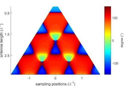
Metasurface microlens focal plane arrays and mirrors
Tam metin
Şekil


Benzer Belgeler
Sıyırma adımında hangi tarama modunun daha duyar ve tekrarlanabilir olduğunu görmek için 1 M HCI ve 50 μg/L arsenik içeren çözelti içerisinde DP ve SW
iflte diyorlar böyle bir filan hamam var flöyle flifal› böyle flifal› ondan sonrada ney- se ondan sonra Oh Baba da geliyor.. Oh
Time course of the decomposition of trap molecules upon irradiation with a 725 nm LED array in the absence (black squares) and presence (red circles) of 5; in IPA using an
Benefit Generosity Index, Comparative Welfare Entitlements Dataset (CWED), Decommodification Index, dependent variable problem, retrenchment, Social Citizenship Indicator
ABSTRACT: Composites of a polypyrrole ( PPy ) and poly ( vinyl chloride – vinyl acetate ) copolymer ( PVC – PVA ) were prepared both chemically and electrochemically.. An insu-
In this paper, we analyze the implications of the proposed measurement device model by considering a non-random vector parameter estimation problem under a constraint on the
Electrospinning is a widely used method to produce nanofibers with unique properties like high surface area to volume ratio and nanoporous structure [5].. These unique
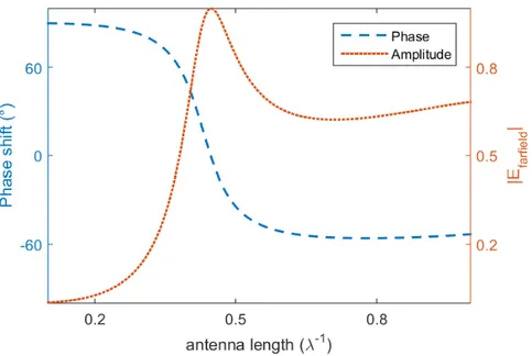
At the surface mode reso- nance frequency the transmitted electromagnetic waves from the subwavelength circular annular aperture surrounded by concentric periodic grooves have a
