Multiscale Self-Assembly of Silicon Quantum Dots into an
Anisotropic Three-Dimensional Random Network
Serim Ilday,
*
,†,‡F. Ömer Ilday,
‡,§Rene
́ Hübner,
∥Ty J. Prosa,
⊥Isabelle Martin,
⊥Gizem Nogay,
#Ismail Kabacelik,
∇Zoltan Mics,
○Mischa Bonn,
○Dmitry Turchinovich,
○Hande Toffoli,
#Daniele Toffoli,
◆David Friedrich,
∥Bernd Schmidt,
∥Karl-Heinz Heinig,
∥and Rasit Turan
#†Department of Micro and Nanotechnology, Middle East Technical University, 06800, Ankara, Turkey
‡Department of Physics and §Department of Electrical and Electronics Engineering, Bilkent University, 06800, Ankara, Turkey
∥Institute of Ion Beam Physics and Materials Research, Helmholtz-Zentrum Dresden-Rossendorf, D-01328 Dresden, Germany
⊥CAMECA Instruments Inc., Madison, Wisconsin 53711 United States
#Department of Physics, Middle East Technical University, 06800, Ankara, Turkey
∇Department of Physics, Akdeniz University, 07058, Antalya, Turkey
○Max Planck Institute for Polymer Research, Ackermannweg 10, 55128 Mainz, Germany
◆Dipartimento di Scienze Chimiche e Farmaceutiche, Universita di Trieste, Via L. Giorgieri 1, 34127 Trieste, Italy
*
S Supporting InformationABSTRACT: Multiscale self-assembly is ubiquitous in nature but its deliberate use to synthesize multifunctional three-dimensional materials
remains rare, partly due to the notoriously difficult problem of controlling
topology from atomic to macroscopic scales to obtain intended material properties. Here, we propose a simple, modular, noncolloidal methodology that is based on exploiting universality in stochastic growth dynamics and driving the growth process under far-from-equilibrium conditions toward a
preplanned structure. As proof of principle, we demonstrate a con
fined-but-connected solid structure, comprising an anisotropic random network of silicon quantum-dots that hierarchically self-assembles from the atomic to the microscopic scales. First, quantum-dots form to subsequently
interconnect without inflating their diameters to form a random network,
and this network then grows in a preferential direction to form undulated
and branching nanowire-like structures. This specific topology
simulta-neously achieves two scale-dependent features, which were previously thought to be mutually exclusive: good electrical conduction on the microscale and a bandgap tunable over a range of energies on the nanoscale.
KEYWORDS: Si, random network, hierarchical, multiscale, self-assembly, stochastic deposition
O
ne of the well-known challenges in the design ofnanomaterials is to simultaneously achieve material properties originating from few-atom scale and resulting in bulk properties through which the material connects to other
materials or interacts with devices.1−3This is difficult because
properties arising from physics at different scales are often
mutually exclusive.4,5 Topology and material properties are
intimately coupled and certain topologies with higher complex-ity, such as interconnected networks of low-dimensional
quantum-confined structures, can give rise to fundamentally
different material characteristics.1,3−8 They can even exhibit
completely new features, which are absent in their individual constituents, but emerge from their collective interactions as
defined in part by their topology.1,4,5,9,10However, it is rarely
clear a priori how such a topology should look like in order to
solve a given problem and typically it is even more difficult to
fabricate that particular topology. Top-down approaches
require numerous complex steps and high-precision control over virtually all degrees of freedom for fabrication of such multiscale, multifunctional materials. These factors render
fabrication techniques not only complex but also highly specific
to the particular material system, which limit compatibility with well-established processing technologies. Self-assembly is an
elegant and potentially simpler alternative,1,5,9,11,12but directing
the self-assembly process toward a preplanned structure is also
notoriously difficult and there is no systematic approach to
determine the experimental procedure for self-assembly of a given structure. Consequently, self-assembly based solutions
also tend to be highly material specific.
Received: December 17, 2015 Revised: February 8, 2016 Published: February 11, 2016
pubs.acs.org/NanoLett
Downloaded via BILKENT UNIV on December 23, 2018 at 17:31:14 (UTC).
A prototypical and also technologically important example is
the 30-year-old challenge of realizing a connected-but-confined
silicon nanostructure embedded in a dielectric matrix (e.g.,
SiO2) that combines quantum-dot-like optical properties and
good electrical conduction:6,13,14 These properties are
seem-ingly contradicting because charge confinement goes
hand-in-hand with localization. While there is a large body of work on
confined-but-connected quantum-dots,15,16 this has not been
demonstrated in a Si system except for the demonstration of
quantum confinement effects above the percolation threshold.17
Porous Si has also shown to exhibit confinement and
connectedness, however, with poor electrical conduction and
lack of control over the bandgap.6,13,14This is so because there
are major challenges from materials perspective such as control over the pore sizes and the uniformity of the pores and stability problem due to the high possibility of oxidation under
atmospheric conditions.6,13,14 Moreover, an overwhelming
majority of the studies on confined-but-connected materials
use (functionalized) colloidal particles.15,16,18Apart from being
strongly material specific, the fabrication procedure is also
complicated and requires multiple steps, that is, nanoparticle synthesis, postannealing of the nanoparticles to connect the
dots, recovery of the colloidal film from the solution, and its
cleaning.15,16There is much motivation for the development of
a Si-based material, because Si is the material of choice for optoelectronic and photovoltaic applications by virtue of its low cost, natural abundance, and excellent compatibility with
well-established processing technologies.6,13
The origin of the difficulty of achieving quantum
confine-ment and good electrical conductivity in a Si system is shown
schematically inFigure 1a. Basically, the maximum permissible
Si concentration for which quantum confinement is preserved
is prohibitively low for conductivity with a purely random distribution of the nanocrystals. The limited number of Si atoms in contact prevents the formation of extensive current routes. Consequently, charge transport has to rely on tunneling,
which is extremely inefficient.6,13,14The straightforward remedy
is to increase the Si concentration, thus forming a percolated
crystal network that can provide sufficient routes for efficient
charge transport. This fails since it inadvertently inflates average
nanocrystal sizes beyond the critical Bohr radius (∼5 nm),
resulting in loss of quantum confinement, that is, an
overcrowded network.6,13,14
Here, we set out to address this problem through a tailored material topology that we aimed to create through self-assembly. We did so by using a toy model to determine stochastic growth parameters that would result in the desired topology. We then created and exploited far-from-equilibrium conditions during deposition to shape the stochastic dynamics toward achieving this preplanned topology. Namely, we have created an anisotropic random network of Si quantum dots (QDs). At the atomic scale, QDs are formed under nonequilibrium conditions, which we exploit to prevent full
phase separation of Si and SiO2through stabilizing nominally
unstable suboxides (SiOx). These QDs sparsely interconnect
without inflating their diameters to form an anisotropic random
Figure 1.Conceptual methodology. Sketches of (a) dependence of photoluminescence and electrical conductivity on Si concentration. For regular nanocrystals, Si concentration thresholds of quantum confinement and good conductivity do not overlap. (b) For the random network, a region of a confined-but-connected structure emerges upon pushing and pulling the two thresholds toward each other through promoting vertical growth of the nanocrystals and limiting full phase separation of Si and SiO2. Atom probe tomography (APT) images show 2D projections of the 3D images, where
a random sampling of Si ions (green) is displayed for isolated QDs (forx = 1.29) and anisotropic random network structure (for x = 1.07) on the left- and right-hand-side images, respectively. (c) Schematics of the deposition chamber. (Inset) Incoming hot atoms lose most of their kinetic energy upon collision with the cold substrate and are confined to a local energy minimum within a few nanometers of their impact points. (d) Monte Carlo simulation of microscale topology of the random network, showing its preferentially vertical alignment. Red and cyan dots indicate electrically percolated and isolated Si nanocrystals, respectively.
network, thereby increasing the threshold for quantum
confinement to higher Si concentrations. On larger scales,
this network becomes anisotropic, preferentially growing in the vertical direction to form nanowire-like structures. This particular topology decreases the Si concentration threshold
for electrical percolation (Figure 1b). Therefore, a range of Si
concentration values emerge within which both the
require-ments of quantum confinement and electrical conductivity are
satisfied. We report simultaneous achievement of good
electrical conductivity (∼0.1 S/m) and a bandgap tunable
over the visible light range (from∼1.8 to 2.7 eV).
Because the requirements of good conductivity and quantum
confinement pertain to different length scales, it was logical to
seek a solution in the form of a multiscale structure. In our case, there are two well-known nanostructures that already meet our
requirements, albeit one at a time. Quantum confinement
requires isolated low-dimensional quantum-confined structures, like QDs (0D) and good electrical conductivity can be achieved with well-connected extended structures, like nanowires (1D). Therefore, we aimed for a multiscale topology that can be conceptualized by means of a fusion of these two types of structures.
In order to determine how to self-assemble such a topology, we developed a toy model of the stochastic deposition process (Figure 1c) from which we related the intended topology to only three stochastic growth parameters. According to this
model, Si and SiOx(x is the O/Si ratio and 0 < x < 2) particles
are incident on the surface with a probability ofp1= 1/(1 +x)
and 1− p1, respectively. The value ofp1simply determines the
final ratio of Si to SiOx. Once the particles come into contact
with the surface, they can seek and“stick” to a particle of the
same type, the probability of which is related top2, or they can
“diffuse” regardless of which type of particle they end up
touching with a probability ofp3. The value ofp2relates to the
propensity of the structure to grow in straight vertical lines in a
similar fashion to nanowires. Finally,p3describes the tendency
to branch off. These three probabilities are sufficient to describe
a rich variety of topologies (Figure S1), including the structure
reported here (Figure 1d). Although a toy model such as this
certainly cannot be used for quantitatively accurate modeling, this simplicity is crucial to easily determine the basic requirements to achieve the desired topology through Monte Carlo simulations and then to relate those requirements to
experimental conditions. Higher values of p2 lead to
preferentially vertically oriented growth, meanwhile p3 is kept
low enough to preserve this orientation but not too low to avoid becoming nanowire-like, which is also undesirable. Then, it is straightforward to calculate the ratio of connected to isolated clusters of Si as a function of Si concentration
(determined byp1), which allows approximately 80−90% of the
Si sites to be globally connected forx = 1.0−1.2.
Having qualitatively linked the desired topology to parameters governing stochastic growth with the toy model, the next step was to achieve the corresponding experimental
conditions (Figure 1c). Fabrication was performed using
magnetron sputter deposition. The connection of p1 to
experiments is straightforward and is adjusted through the
ratio of power applied to the Si and SiO2 targets during
deposition. The goal is to utilize the minimum Si concentration that results in a percolated network, the requirement for
efficient conduction. The choice of x is described in detail
below. The deposition parameters and p2 and p3 are less
straightforward to implement experimentally, and these
probabilities have to be regarded as effective values providing
a simplified description of much more complicated dynamics
affected by various experimental parameters. Nevertheless, it is
not difficult to identify effective “knobs” for each of them. The
sticking or affinity of the Si atoms to Si atoms is present during
deposition but occurs also following a postannealing procedure, as evidenced by the fact that the vertical orientation of the network becomes more prominent after postannealing. Thus,
the postannealing process parameters influence propensity to
grow vertically, hence p2. Similarly, lateral diffusion of the
deposited atoms and, effectively, the value of p3is most readily
controlled by the kinetic energy of the particles after hitting the surface and the temperature of the surface. To limit this process, we create a temperature gradient by keeping the
substrate“cold” (at room temperature), while depositing “hot”
particles, which are energized by the magnetrons (inset of
Figure 1c). The kinetic energies of the deposited particles are controlled through magnetron power levels. Following
identification of these basic experimental control knobs, it
was necessary to pursue a laborious but straightforward experimental procedure iterating between fabrication runs and
characterization in order to pin down thefinal set of deposition
parameters until a structure that matches the design was obtained.
There is a second purpose for the spatiotemporal temper-ature gradient on the surface, which is to serve as leverage to meet our second goal of increasing Si concentrations for which
quantum confinement can be maintained. During fast stochastic
deposition, the atoms rain down onto the cold substrate, which forces the adatoms to settle at minimum energy positions within a few nanometers of the collision points, instead of seeking out the global minimum over larger portions of the surface. This way, Si and O atoms are trapped into a random network that is being braided during deposition. Even when a calibrated amount of external energy is introduced into the system (during postannealing to promote crystallization at high temperatures), the atoms are not able to move freely to form
stable Si and SiO2 but they are forced to locally rearrange
themselves that results in locking the unstable suboxides into their nonglobal but local equilibrium states and prevent full
phase separation (Figures S2 and S3).
Normally, when sufficient energy is applied to the system,
suboxides break down and turn into stable forms of either Si or
SiO2 through a disproportionation reaction. The thermal
gradient created by the cold substrate serves to stabilize suboxides, which, in turn push up the Si concentration limit for
quantum confinement. If too many suboxides turn into Si, they
inflate the effective QD diameter, which eventually destroys the
quantum confinement, resulting in an overcrowded network. In
the other extreme, if too many suboxides turn into SiO2, they
surround and isolate the QDs, which once again have to rely on
inefficient tunneling currents for conduction. The key issue
then is to obtain nominally unstable suboxides and to prevent
them from turning into stable forms of Si and SiO2completely
upon addition of external energy, thereby limiting further growth of QD diameters. Creation of far-from-equilibrium conditions, as opposed to merely near-equilibrium, via large spatiotemporal thermal gradients is important in stabilizing the suboxides. This way, a larger number of small-size QDs are obtained instead of a smaller number of large-size QDs in a given volume, which more readily form a percolated network due to increased density of connections.
Having discussed the methodology of the design and
self-assembly, we first present characterization of the multiscale
topology of the network, followed by its electrical and optical properties. The topology of the Si QD network was designed to be anisotropic on the microscale (over tens to hundreds of
nanometers) and isotropic on the nanoscale (up to∼10 nm).
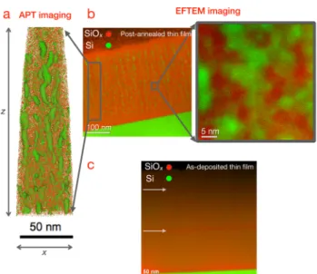
This is verified experimentally through atom probe tomography
(APT) and energy-filtered transmission electron microscopy
(EFTEM).Figure 2a shows 2D projection of a 3D APT image
of the random network, where a random sampling of the Si ions
(green) and O ions (red) is displayed (see also theSupporting
Movie). The APT analysis establishes the vertical orientation unambiguously, which is also discernible from the EFTEM
images.Figure 2b shows pseudocolored superposition of the Si
(green) and SiOx(red) EFTEM image of the random network
of Si QDs that is oriented preferentially in the vertical direction
resembling nanowires and the magnified image displays
interconnected Si QDs with∼2 nm average diameters (Figure
S4) that are embedded inside the SiOxmatrix.
The EFTEM and APT data suggest that many of the Si QDs
are in physical contact with each other without any SiOx
between them, as predicted by the Monte Carlo simulations. This has profound implications for charge transport; charge can be transported directly without relying on tunneling. In order to ascertain that this is the case, we have applied a tomography technique, whereby spatial distributions of Si QDs and the
surrounding amorphous SiOx matrix were determined
sepa-rately by energy filtering analysis (Figure S5). Additional
diffraction analysis was used to prove that there are distinct Si
nanocrystals, which are directly touching each other without
any SiOx in between.
We have mentioned above that the vertical orientation of the network becomes more pronounced after postannealing as this
process triggers a limited degree of Si mobility and tendency to stick together. In order to rule out the possibility that the preferential vertical growth could be solely the result of a postannealing procedure, a test specimen has been prepared and was analyzed by EFTEM directly after magnetron sputter deposition without any postannealing procedure as shown in
Figure 2c. During deposition of this test sample, sputtering from the Si target was interrupted twice to ensure that the directional growth could reinitiate, as would be expected, considering that the growth is stochastic and obeys the rules we
have predetermined to control surface diffusion. As seen in
Figure 2c, two thin red layers comprising only suboxides (areas pointed by two arrows) appear after which the vertical growth of Si has continued in the same manner. We further observe that the network is already anisotropic (albeit less pronounced) even though no postannealing was performed on this sample.
The desired large-scale anisotropy of the QD network topology is achieved for a range of Si concentrations, which we refer to as the network region. Si concentrations that delimit this interesting region from below and above are similarly
referred to as the “prenetwork” and “postnetwork” regions.
Within this range, the average QD diameters can be controlled
through adjustment of the Si concentration. This is confirmed
through EFTEM images shown in Figure 3. Nanocrystal
diameters increase and the morphology becomes more wire-like
when Si concentration is increased (when x decreases from
1.07 to 0.95).
Figure 4a shows a typical magnified APT image of the random network. The image reveals that although the network structure somewhat resembles nanowires on the microscale, the vertical lines are far from being straight and they can be referred Figure 2. Structural and morphological analyses. (a) The 2D
projections of 3D APT images, where a random sampling of the Si ions (green) and O ions (red) are displayed for anisotropic random network structure (forx = 1.07). Superposition of the Si (green) and the SiOx (red) plasmon EFTEM images showing (b) preferential
growth of the network along the vertical direction on the microscale and (inset) percolated Si QD network inside a SiOx matrix on the
nanoscale for anisotropic random network structure (forx = 1.07) and (c) vertical orientation of Si atoms before any postannealing procedure is applied (forx = 1.07).
Figure 3. Superposition of the cross-sectional Si (green) and SiOx
(red) plasmon EFTEM images show how QD diameters in the random network structure changes with respect to increased Si concentration (fromx = 1.07 to x = 0.95).
to as“wires” only as a crude approximation. They are rather heavily undulated, frequently interconnecting and branching.
The effective wire diameters vary spatially as pointed out by
markings inFigure 4a. This specific topology has implications
for charge transport and photoemission with subtly different
characteristics for charges that are locally generated through the
photoelectric effect and for those that are injected externally
through the electrodes (seeSupporting Information).
Photoelectrons are generated only at sites where a photon is
absorbed, which is more likely to occur at quantum-confined
sites. Therefore, strong PL emission signal is expected for the prenetwork region comprising mostly isolated QDs. For the postnetwork region, PL signal will vanish as a result of nearly
complete loss of confinement within a bulklike crystalline
structure. PL signal is expected to decrease upon emergence of an interconnected random network because free charge carriers will belong to a cluster of QDs, which increases the probability of charge carrier pair separation because they are free to move
to larger distances.8,19−21 This de facto decreases the
probability of recombination of the charge carrier pair.8,19−21
However, thanks to the network being sparely connected,
quantum confinement will be preserved on average, resulting in
a less intense but still strong PL emission. These expectations
are confirmed by the PL measurements as shown inFigure 4b.
Control of the average QD diameter in the network topology
naturally affords us the important capability of tuning the
optical bandgap of the random network from ∼1.8 to 2.7 eV,
covering most of the visible spectrum, as confirmed
experimentally (Figure 4b,c). Although the bandgap values
and PL emission energies are consistent and within the nominal
values for quantum-confined Si nanostructures,6,13,22−25there is
a shift between the bandgap values calculated from the optical
absorption (Figure 4c) and the PL emission spectra (inset of
Figure 4b). Previous studies reported this phenomena to be the
influence of exciton binding energy and/or Stokes-shift
(depending on the material topology and nanocrystal-matrix
interface) for Si nanostructures13,23−25 as well as for other
nanomaterials.26−28
Of particular interest is the observation of percolation through direct current conductivity measurements, because percolation provides an intellectual bridge between structural information, which is a locally determined property of a network and electrical characteristics that are determined
collectively by the entire network.29Furthermore, percolation
behavior is often robust against variations in many parameters
or characteristics as long as the topology remains unchanged.29
Results of current−voltage (I−V) conductivity measurements
are shown inFigure 4d. As expected, when the Si concentration
is increased, conductivity increases abruptly after a critical value
of x in both lateral and vertical directions is exceeded, which
corresponds to a Si concentration below the nominal
percolation threshold (xc=∼1) of Si in a SiOxmatrix.8,19,29,30
Conductivity values approaching the percolation threshold,xc,
from above were fit by σ ∼ (xc− x)t, where t is the critical
percolation exponent.8,19,29,30The estimated values ofxc= 1.29
andt = 2.0 for vertical conductivity, and xc= 1.18 andt = 1.3
for lateral conductivity. The observation of a lower percolation threshold for the vertical direction than the lateral direction is an independent proof of the anisotropic structure. We note that the critical exponents for vertical and lateral conductivity Figure 4.Quantum confinement and percolation analyses. (a) APT image shows undulated and branching wirelike morphology of the random network (for x = 1.07) where the wire diameter differentiate spatially. The externally connected Si QD cluster is colored pink and internally connected but externally isolated clusters are colored gray (circled in dash lines). (b) Graph showing a highly intense PL signal for the prenetwork region, a reduced PL signal intensity for the network region, and virtually zero PL signal for the postnetwork region. (Inset) Graph showing full PL spectra for the three regions. (c) Graph showing tunable bandgap from prenetwork to network and postnetwork regions. (d) Graph showing percolation analyses and electrical conductivity in the lateral and vertical directions for prenetwork, network, and postnetwork regions. Insetfigures showing cartoons of the devices used to conduct lateral (bottom image) and vertical (top image)I−V measurements.
closely match the universal values for 3D and 2D conduction
networks, respectively.8,19,29,30 This direction-dependent
di-mensionality is remarkable, but not surprising, given the topology of the network. For conductivity in the lateral direction, as additional conducting nodes are added (decreasing x), few of those that are along the vertical direction contribute to conductivity along the lateral direction, because many of
them efficiently lead above or below the lateral plane.
Consequently, the percolation characteristics are expected to be closer to that of a nominally 2D network. In other words,
the anisotropy effectively reduces the dimensionality of the
network for conductivity along this direction. In contrast, the percolation behavior along the vertical direction better matches that of a 3D network, because additions of conducting nodes contribute to conduction along the vertical direction similarly. In conclusion, we propose a simple methodology based on exploiting universality in stochastic growth dynamics and use of physical forces, such as thermal gradients and control of chemical interactions, to achieve self-assembly of a preplanned structure. We applied our approach to the design and fabrication of a nanostructured Si-based material, which brings together QD-like optical properties and good electrical
conduction as Priolo et al. envisioned6 with possible
applications in Si photonics,6,8,31,32 photovoltaics,6−8,14,15,31,32
and optoelectronics.6−8,31,32 Our design procedure utilized a
toy model that links desired topology to effective stochastic
growth parameters for the self-assembly process. We have qualitatively related the growth parameters to the experimental parameters with the help of the model and determined their
specific values experimentally. Given the simplicity of this
methodology, it is reasonable to expect that the present approach of utilizing universality of stochastic growth dynamics toward creation of a multiscale topology can be adapted to
different material systems that can benefit from multiscale
self-assembled structures. Experimentally, the resulting structure is not only robust after exposure to air for more than a year but also survives prolonged annealing at high temperatures. Furthermore, it is highly uniform within a sample and reproducible from sample to sample. We have characterized its optical and electrical responses, which provide an
independent confirmation of the multiscale topology. In
particular, the latter has revealed that motion of the charge is microscopically anisotropic but nanoscopically isotropic. Apart from a number of possible photonic and optoelectronic
applications, our findings suggest that this complex random
network may also be used in biophotonics,32 imaging
technologies,32 Li-ion batteries,32,33 and chemical and
bio-medical sensors.34
■
ASSOCIATED CONTENT*
S Supporting InformationThe Supporting Information is available free of charge on the
ACS Publications website at DOI: 10.1021/acs.nano-lett.5b05158.
Methods, detailed calculations and simulations, and detailed information on the chemical, structural, optical.
and electrical analyses. (PDF)
APT image of random network where random sampling of the Si ions (green) and O ions (red) is displayed.
(AVI)
■
AUTHOR INFORMATIONCorresponding Author
*E-mail:[email protected].
Author Contributions
S.I. conceived of and conducted the experiments. S.I. and F.Ö.I. developed the stochastic deposition model and wrote the paper. F.Ö.I. performed the MC simulations. R.H. conducted TEM, T.J.P,. and I.M. conducted APT imaging and analyses. S.I., G.N., and I.K. performed electrical analyses. Z.M., D.T., and M.B. conducted THz spectroscopy analyses. H.U. and D.T. conducted MD simulations. D.F. conducted RBS analyses and assisted in TEM imaging. B.S. and K.H.H. supervised TEM imaging and RBS analyses. R.T. supervised the study.
Funding
This work was supported by the Scientific and Technological
Research Council of Turkey (TÜBİTAK) and the German Federal Ministry of Education and Research (BMBF) with Grant 109R037. F.Ö.I. also acknowledges support from the European Research Council (ERC) Consolidator Grant ERC-617521 NLL.
Notes
The authors declare no competingfinancial interest.
■
ACKNOWLEDGMENTSThe authors thank to İlker Yıldız and Seçkin Öztürk for their
contributions to XPS and early HRTEM analyses, respectively, and to Alexandre Houssou and Dr. Olivier Dulac for their contributions in APT analyses.
■
REFERENCES(1) Boal, A. K.; Ilhan, F.; DeRouchey, J. E.; Thurn-Albrecht, T.; Russell, T. P.; Rotello, V. M.Nature 2000, 404, 746−748.
(2) Lopinski, G. P.; Wayner, D. D. M.; Wolkow, R. A.Nature 2000, 406, 48−51.
(3) Tavakkoli, A. K. G.; Gotrik, K. W.; Hannon, A. F.; Alexander-Katz, A.; Ross, C. A.; Berggren, K. K.Science 2012, 336, 1294−1298.
(4) Hammond, P. T.Adv. Mater. 2004, 16, 1271−1293. (5) Mann, S.Nat. Mater. 2009, 8, 781−791.
(6) Priolo, F.; Gregorkiewicz, T.; Galli, M.; Krauss, T. F. Nat. Nanotechnol. 2014, 9, 19−32.
(7) Escarcega-Bobadilla, M. V.; Zelada-Guillen, G. A.; Pyrlin, S. V.; Wegrzyn, M.; Ramos, M. M. D.; Gimenez, E.; Stewart, A.; Maier, G.; Kleij, A. W.Nat. Commun. 2013, 4, 2648.
(8) Nie, Z.; Petukhova, A.; Kumacheva, E.Nat. Nanotechnol. 2010, 5, 15−25.
(9) Jia, G.; Sitt, A.; Hitin, G. B.; Hadar, I.; Bekenstein, Y.; Amit, Y.; Popov, I.; Banin, U.Nat. Mater. 2014, 13, 301−307.
(10) Damasceno, P. F.; Engel, M.; Glotzer, S. C.Science 2012, 337, 453−457.
(11) Whitesides, G. M.; Grzybowski, B.Science 2002, 295, 2418− 2421.
(12) Zhao, Y.; Thorkelsson, K.; Mastroianni, A. J.; Schilling, T.; Luther, J. M.; Rancatore, B. J.; Matsunaga, K.; Jinnai, H.; Wu, Y.; Poulsen, D.; Fréchet, J. M. J.; Alivisatos, A. P.; Xu, T. Nat. Mater. 2009, 8, 979−985.
(13) Pavesi, L.; Turan, R. Si Nanocrystals: Fundamentals, Synthesis, and Applications; Wiley-VCH Verlag GmbH & Co.: Berlin, 2010.
(14) Balberg, I.; Jedrzejewski, J.; Savir, E. Phys. Rev. B: Condens. Matter Mater. Phys. 2011, 83, 035318.
(15) Baumgardner, W. J.; Whitham, K.; Hanrath, T.Nano Lett. 2013, 13, 3225.
(16) Evers, W. H.; Schins, J. M.; Aerts, M.; Kulkarni, A.; Capiod, P.; Berthe, M.; Grandidier, B.; Delerue, C.; van der Zant, H. S. J.; van Overbeek, C.; Peters, J. L.; Vanmaekelbergh, D.; Siebbeles, L. D. A. Nat. Commun. 2015, 6, 8195.
(17) Wolf, O.; Millo, O.; Balberg, I.J. Appl. Phys. 2013, 113, 144314. (18) Milliron, D. J.; Hughes, S. M.; Cui, Y.; Manna, L.; Li, J.; Wang, L.-W.; Alivisatos, A. P.Nature 2004, 430, 190−195.
(19) Balberg, I.; Savir, E.; Jedrzejewski, J.; Nassiopoulou, A. G.; Gardelis, S. Phys. Rev. B: Condens. Matter Mater. Phys. 2007, 75, 235329.
(20) Cox, T. I.; Simons, A. J.; Loni, A.; Calcott, P. D. J.; Canham, L. T.; Uren, M. J.; Nash, K. J.J. Appl. Phys. 1999, 86 (5), 2764−2773.
(21) Keles, U.; Cakan, A.; Bulutay, C. J. Appl. Phys. 2015, 117, 064308.
(22) Tomozeiu, N.Optoelectronics-Materials and Techniques; InTech: Rijeka, Croatia, 2011; Chapter 3.
(23) Pavesi, L.; Gaponenko, S.; Dal Negro, L. Towards the First Silicon Laser; Springer: Trento, Italy, 2002.
(24) Di, D.; Xu, H.; Perez-Wurfl, I.; Green, M. A.; Conibeer, G. Nanoscale Res. Lett. 2011, 6, 612.
(25) Le, T.-H.; Jeong, H.-D.Bull. Korean Chem. Soc. 2014, 35, 1523. (26) Prasad, A. V.; Misra, P.; Ahirwar, G.Res. J. Phys. Sci. 2013, 1, 11−14.
(27) So, D.; Konstantatos, G.Chem. Mater. 2015, 27, 8424−8432. (28) Ahmad, S.; Baumberg, J. J.; Prakash, G. V.J. Appl. Phys. 2013, 114, 233511.
(29) Stauffer, D.; Aharony, A. Introduction to Percolation Theory; Taylor & Francis: London, 1992.
(30) Manna, L.; Milliron, D. J.; Meisel, A.; Scher, E. C.; Alivisatos, A. P.Nat. Mater. 2003, 2, 382−385.
(31) Gudiksen, M. S.; Lauhon, L. J.; Wang, J.; Smith, D. C.; Lieber, C. M.Nature 2002, 415, 617−620.
(32) Dasgupta, N. P.; Sun, J.; Liu, C.; Brittman, S.; Andrews, S. C.; Lim, J.; Gao, H.; Yan, R.; Yang, P.Adv. Mater. 2014, 26, 2137−2184. (33) Bogart, T. D.; Oka, D.; Lu, X.; Gu, M.; Wang, C.; Korgel, B. A. ACS Nano 2014, 8, 915−922.
(34) Cui, Y.; Wei, Q.; Park, H.; Lieber, C. M. Science 2001, 293, 1289−1292.