ScienceDirect
Materials Today: Proceedings 18 (2019) 1996–2002 www.materialstoday.com/proceedings
2214-7853 © 2019 Elsevier Ltd. All rights reserved.
Selection and/or Peer-review under responsibility of INTERNATIONAL CONGRESS ON SEMICONDUCTOR MATERIALS AND DEVICES.
ICSMD-2017
Investigation of Conversion Efficiency of n-ZnO/p-Si
Heterojunction Device Produced by Pulsed Laser Deposition (PLD)
Serap Yiğit Gezgin
a, Abdullah Kepceoğlu
a, Ahmet Toprak
a, Hamdi Şükür Kılıç
a,b,*aSelçuk University, Faculty of Science, Department of Physics, 42000, TURKEY bSelçuk University, High Technology Research and Application Center, 42000, TURKEY
Abstract
In this study, n-ZnO/p-Si heterojunction was produced by growing polycrystalline Zinc Oxide (ZnO) thin films on p-type Si (100) substrate at 500 μm thickness using Pulsed Laser Deposition (PLD) method. The crystalline and morphologic structure of ZnO thin film were analysed by X-ray diffraction (XRD) and Atomic Force Microscopy (AFM) techniques. The photovoltaic (PV) property of n-ZnO/p-Si heterojunction was investigated by using current-voltage (J-V) measurement under illumination at 70 mW/cm2. The silver (Ag) metal thin film was deposited by PLD to make ohmic contacts to the n-ZnO/p-Si heterojunction structure. The barrier height and the ideality factor were calculated to be 0.51 eV and 12.37, respectively, at room temperature (RT). The largest values of open circuit voltage (Voc) and short circuit current density (Jsc) were about 250 mV and 1.63 mA/cm2, respectively. The photoelectric conversion efficiency in the range of 0.12% have been achieved and presented in this paper.
© 2019 Elsevier Ltd. All rights reserved.
Selection and/or Peer-review under responsibility of INTERNATIONAL CONGRESS ON SEMICONDUCTOR MATERIALS AND DEVICES.
Keywords: PLD; heterojunction; ZnO; Si; efficiency
* Corresponding author. Tel.: +90-5333652174; fax:+90-332 241 24 99. E-mail address: [email protected]
1. Introduction
ZnO thin film used as n-type transparent conductive oxide (TCO) layer in heterojunction devices is a promising semiconductor material (with II-VI components) for advanced optoelectronic applications due to its wide direct band gap (3.37 eV), large exciton binding energy (60 meV), high electron mobility, good transparency, high thermal and mechanical stability, low cost, non-toxicity and demand to relatively low deposition temperature [1, 2]. ZnO is an excellent semiconductor and has potential applications such as diodes, photovoltaic devices, liquid crystal displays (LCDs), light emitting diodes (LEDs), sensors and actuators [1, 3-5]. One major issue in the solar cell industry is the high costs, ZnO has a great advantage in terms of cost reduction[6]. In addition, p-Si wafer, which is used as an active layer in the n-ZnO/p-Si heterojunction structure in this study, is an inexpensive, excellent quality, low band gap (1.1 eV), large-area available, nature friendly, compatibility with ZnO crystal structure material [3]. Briefly, n-ZnO/p-Si heterojunciton have some potential advantages such as high abundant material and excellent n-type transparent oxide layer, simple processing steps and low processing temperature . All of these advantages make ZnO/Si hetero-junction alternative candidate in the future photovoltaic (PV) market industry.
The coating technics such as magnetron sputtering, molecular beam epitaxy (MBE), PLD, sol-gel process are all used to produced thin film growth [7]. The PLD technique for transparent conductive oxide (TCO) thin film has a great advantages compared to other techniques. The crystalline, stoichiometric epitaxial TCO thin films can be produced by PLD at low substrate temperatures in the oxygen gas ambient [8, 9]. In this study, we deposited polycrystalline ZnO thin films on p-Si substrate at RT using PLD. Furthermore, the silver based (Ag) front fingers on emiter side and back contacts were deposited by PLD.
In this study, morphological characteristic and the crystal structure of ZnO thin film grown on p-type silicon was investigated by AFM and XRD, respectively. Its optical properties were examined by UV-VIS range. In addition, the conversion efficiency of n-ZnO/p-Si heterojunction solar cell were calculated from the obtained J-V measurements. The factors affecting the efficiency of device have been discussed.
2. Materials and Method
ZnO thin film was grown on p-Si (100) have 8-12 Ω.cm resistivity and on the microscope slide glass by Pulsed Laser Ablation (PLA) using a Nd:YAG laser (Continuum, Minilite II) system which is operated in pulsed mode and produces laser pulses with 45 mJ at 5 ns pulse width at 10 Hz repetition rate at the wavelength of 1064 nm. ZnO sputter target (99.99% purity, Beijing Goodwill Metal, China) was used as target material. 100 oriented p-type Si
wafer having a 500 μm thickness in 1 cm2 area was used as substrate. The distance between the target and substrate
was 50 mm. The target and substrate holders are rotated at a certain rate for the target material not to be damaged
and homogeneity for thin film. Before the experiments begin, base pressure was 1×10⁻⁶ mbar. The laser beam was
focused on the ZnO target with a 40 cm focal length biconvex lens. n-type ZnO thin film was deposited by laser
pulses carrying 45 mJ energy in an ambient oxygen environment at a pressure of 1.3×10⁻¹ mbar. The mask is
produced by micromachining method using femtosecond (fs) laser pulses to form front finger contact. Ag thin film
was deposited for ohmic back contact formation under 1×10⁻⁶ mbar vacuum conditions and as a front finger contact
on ZnO thin film (in the Argon gas pressure at 8×10⁻² mbar) with ablation of Ag material (99.99% purity, Kurt
Lesker) by 45 mJ laser pulse.
3. Results and Discussion
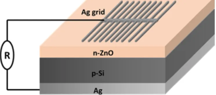
The schematic representation of Ag/n-ZnO/p-Si/Ag heterojunction structure is shown in fig. 1. The Ag thin film grown on back surface of p-Si wafer deposited by PLD technique in a thickness of 200 nm and exhibits an ohmic properties. The finger grids are used minimized to avoid shading in the solar cells. However, the finger width should not much narrow and the number of fingers must be increased to collect more charge and provide high current. That’s why, the number, interspace, width, length of the Ag finger front contact was set at 32, 400 μm, 100
Fig. 1. The structure of the Ag/n-ZnO/p-Si/Ag heterojunction PV device.
3.1. The structural and optical properties of ZnO thin film
The 2D and 3D AFM images of n-ZnO thin film produced as a buffer layer on the Si wafer is shown in fig. 2.
According to AFM image of 10 μm2 area in fig. 2, particles forming ZnO thin film are dispersed homogeneously.
The particles are dense and tend to form compact film. The average roughness value is about 5.9 nm and thickness of ZnO thin film is about 70 nm.
According to XRD spectrum in fig. 3, hexagonal ZnO thin film has polycrystalline structure with sharp peaks having (100), (002), (101) directions[1, 3]. ZnO thin film grown on p-Si wafer at RT by PLD and has crystal structure (not showing amorphous properties) which is a suitable condition for emitter layer at pn heterojunction solar cells.
a)
b)
Fig. 3. The XRD spectrum of ZnO thin film.
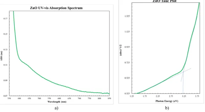
According to the absorption spectrum of ZnO thin film which is presented in fig. 4(a), ZnO thin film has transparency from visible to near-infrared (NIR) region.
The band gap (Eg) of ZnO thin film was determined by Tauc law in equation (1):
( ) = (1)
where, is a constant, is photon energy, is the band gap value which is obtained by extrapolation of linear
portion of ( ) versus plot as seen in fig. 4b. The energy band gap of ZnO thin film was determined to be 3,2
eV which is in well agreement with literature [3, 10].
a) b)
3.2. Current density-voltage characteristics of Ag/n-ZnO/p-Si/Ag
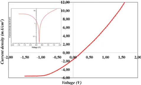
Fig. 5 shows the current density–voltage (J-V) characteristic of n-ZnO/p-Si heterojunction under illumination at RT. It is given the semi–logarithmic forward bias J–V characteristic with an inset in Fig. 5. According to the J-V characteristic, the heterojunction structure shows rectifying behavior.
Fig. 5. J-V graphic of n-ZnO/p-Si heterojunction.
J-V relation of n-ZnO/p-Si heterojunction can be analysed as a function of applied voltage (V) by the expression:
= 1 (2)
where is saturation current density, is electronic charge, is applied voltage, is ideality factor, is
Boltzman’s constant and is temperature in K. The value of is determined to be 3×10⁻³ mA/cm2 from straight
line of versus plot. is the ideality factor which can be written by using eq.(3) and calculated to be 12.37
using
= ( ) (3)
Since the ideality factor is larger than one, n-ZnO/p-Si heterojunction structure exhibits a non-ideal rectifying
behaviour. , the barrier height is defined as:
= (4)
where is the Richardson constant, is the contact area. The values of is 32 Acm-1K-2 for p-Si. The barrier
height, , is calculated to be 0.51 eV which is slightly smaller than its ideal barrier height value which is
difference between work functions of Si (4.97 eV) and ZnO (4.25 eV) [10].
The current under forward bias is slightly higher than that obtained under the reverse bias. Therefore, n-ZnO/p-Si heterojunction exhibits a weak diode behavior and the ideality factor is higher which can be based to the interface
states[11],[2, 7, 12]. Also, the carrier losses in the space charge range (SCR), the tunneling current[13-16] . The
defects of crystal structure and the lower carrier mobility of ZnO thin film, the pinholes formed in ZnO thin film, the contacts can not act ohmic, and the lattice mismatch between ZnO and Si[1, 17] which may lead to the higher
ideality factor. In particular, the charge carriers can overcome the barrier at the low height[3, 18-20]. This situation may have causes a saturation current, , density to be slightly larger under reverse bias, and therefore, the ideality factor was found to be high.
3.3. The photoelectric property of Ag/n-ZnO/p-Si/Ag heterojunction
n-ZnO/p-Si device exhibits a photoelectric behaviour under a 70 mW/cm2 power density illumination. The
values of the short-circuit current density ( ), the open-circuit voltage ( ), the current density at maximum
output ( ), the voltage at maximum output ( ) of n-ZnO/p-Si heterojunction based on solar cell measurements are all shown in the Table 1.
Table 1. The values of parameters n-ZnO/p-Si heterojunction based on solar cell measurements
Parameters for Solar cell measurement
Values
Jsc(short-circuit current density)
Voc(open-circuit current)
Jm (current density at maximum output)
Vm ( voltage at maximum output)
(power conversion efficiency)
1,63 mA/cm2
250 mV
0,99 mA/cm2
100 mV 0.12%
Fill Factor (FF) is used to determine maximum power which is a ratio of the real output ( × ) to the product
of ( × ) in solar cell:
= ×× (5)
Here, we have found as 0.24. The power conversion efficiency of Ag/n-ZnO/p-Si/Ag heterojunction diode are
calculated by courtesy of,
= (6)
where is the input power. The power conversion efficiency ( ) was found to be 0.12%. A higher ideality factor
is an effective parameter for a low conversion efficiency. So, interface situations are very effective in generating leakage current in the depletion region. Undesired charge transitions in the depletion region causes an unwanted leakage current which causes recombination in the depletion region. Because of reduction in the charge separation in this region, the and the efficiency is found to be lower. The contacts can not exhibit ideal ohmic behavior, very narrow SCR, the lower barrier height which may result in the lower efficiency. ZnO is a polycrystalline thin film and presents a disadvantage for the efficiency[21]. To remove this problem, by increasing the substrate temperature during the thin film production process, and by annealing the thin film at the specific temperature, (002) main peak can be more dominant and the efficiency can be increased.
4. Conclusions
In this study, we have produced an Ag/n-ZnO/p-Si/Ag heterojunction diode by PLD method. The band gap of ZnO thin film was measurement to be 3,2 eV. ZnO thin film has a polycrystalline structure with (100), (002), (101) orientations. The ideality factor and the barrier height of n-ZnO/p-Si heterojunction are calculated to be 12.37 and 0.51 eV, respectively. n-ZnO/p-Si heterojunction structure exhibits non-ideal rectifying behavior and diode property. Furthermore, the efficiency of Ag/n-ZnO/p-Si/Ag heterojunction diode is 0.12% under the lamp
illumination of 70 mW/cm2 power density. The high ideality factor and the low efficiency may be caused by the
film, the pinholes formed in ZnO thin film, the lower carrier mobility of ZnO, the tunneling current and the lattice mismatch between ZnO thin film and Si wafer.
Acknowledgements
Authors kindly would like to thank,
- Scientific and Technical Research Council of Turkey (TUBITAK) for financial support via Grant No.
1649B031503748,
- Scientific Research Projects Coordination Unit of Selçuk University for financial support via Projects Nos.
14401087, 13301022 and
- Selçuk University, High Technology Research and Application Center for supplying with Infrastructure.
The data presented in this work will be as a part of Ph.D. thesis of the Serap YİĞİT GEZGİN.
References
[1] S. Sharma and C. Periasamy, "A study on the electrical characteristic of n-ZnO/p-Si heterojunction diode prepared by vacuum coating technique," Superlattices and Microstructures, vol. 73, pp. 12-21, 2014.
[2] L. Shen, Z. Ma, C. Shen, F. Li, B. He, and F. Xu, "Studies on fabrication and characterization of a ZnO/p-Si-based solar cell,"
Superlattices and microstructures, vol. 48, no. 4, pp. 426-433, 2010.
[3] S. Chirakkara and S. Krupanidhi, "Study of n-ZnO/p-Si (100) thin film heterojunctions by pulsed laser deposition without buffer layer,"
Thin Solid Films, vol. 520, no. 18, pp. 5894-5899, 2012.
[4] C. Bozkaplan, "Ag/ZnO/p–Si YAg/ZnO/p–Si Yapısının Elektriksel Karakterizasyonu," FEN BİLİMLERİ ENSTİTÜSÜ MÜDÜRLÜĞÜ, T.C. Dicle Üniversitesi, Diyarbakır, 2011.
[5] A. A. Yousif, "Current transport studies of n-ZnO/p-Si hetero-nanostructures grown by pulsed laser deposition," Int. J. Appl. Innov. Eng.
Manag., vol. 3, 2014.
[6] R. Pietruszka et al., "Photovoltaic properties of ZnO nanorods/p-type Si heterojunction structures," Beilstein journal of nanotechnology, vol. 5, p. 173, 2014.
[7] F. Yakuphanoglu, "Electrical characterization and device characterization of ZnO microring shaped films by sol–gel method," Journal of
Alloys and Compounds, vol. 507, no. 1, pp. 184-189, 2010.
[8] N. Batra, M. Tomar, P. Jain, and V. Gupta, "Laser ablated ZnO thin film for amperometric detection of urea," Journal of Applied Physics, vol. 114, no. 12, p. 124702, 2013.
[9] Y. Inoue, M. Okamoto, T. Kawahara, Y. Okamoto, and J. Morimoto, "Thermoelectric properties of amorphous zinc oxide thin films fabricated by pulsed laser deposition," Materials transactions, vol. 46, no. 7, pp. 1470-1475, 2005.
[10] E. Keskenler et al., "Growth and characterization of Ag/n-ZnO/p-Si/Al heterojunction diode by sol–gel spin technique," Journal of Alloys
and Compounds, vol. 550, pp. 129-132, 2013.
[11] F. Yakuphanoglu, Y. Caglar, M. Caglar, and S. Ilican, "ZnO/p-Si heterojunction photodiode by sol–gel deposition of nanostructure n-ZnO film on p-Si substrate," Materials Science in Semiconductor Processing, vol. 13, no. 3, pp. 137-140, 2010.
[12] A. Ibrahim and A. Ashour, "ZnO/Si solar cell fabricated by spray pyrolysis technique," Journal of Materials Science: Materials in
Electronics, vol. 17, no. 10, pp. 835-839, 2006.
[13] O. Breitenstein, P. Altermatt, K. Ramspeck, and A. Schenk, "The origin of ideality factors n> 2 of shunts and surfaces in the dark IV curves of Si solar cells," in Proceedings of the 21st European Photovoltaic Solar Energy Conference, 2006, pp. 625-628: WIP.
[14] J. M. Shah, Y.-L. Li, T. Gessmann, and E. Schubert, "Experimental analysis and theoretical model for anomalously high ideality factors (n≫ 2.0) in AlGaN/GaN pn junction diodes," Journal of Applied Physics, vol. 94, no. 4, pp. 2627-2630, 2003.
[15] J. Verschraegen, M. Burgelman, and J. Penndorf, "Temperature dependence of the diode ideality factor in CuInS2-on-Cu-tape solar cells,"
Thin Solid Films, vol. 480, pp. 307-311, 2005.
[16] Z. Wang, Z. Cheng, A. E. Delahoy, and K. K. Chin, "A Study of light-sensitive ideality factor and voltage-dependent carrier collection of cdte solar cells in forward bias," IEEE Journal of Photovoltaics, vol. 3, no. 2, pp. 843-851, 2013.
[17] N. Al-Hardan, M. A. Hamid, N. M. Ahmed, R. Shamsudin, and N. K. Othman, "Ag/ZnO/p-Si/Ag heterojunction and their optoelectronic characteristics under different UV wavelength illumination," Sensors and Actuators A: Physical, vol. 242, pp. 50-57, 2016.
[18] F. Bedia, A. Bedia, B. Benyoucef, and S. Hamzaoui, "Electrical characterization of n-ZnO/p-Si heterojunction prepared by spray pyrolysis technique," Physics Procedia, vol. 55, pp. 61-67, 2014.
[19] A. N. Corpus-Mendoza, M. De Souza, and F. Hamelmann, "Transport mechanisms and effective Schottky barrier height of ZnO/a-Si: H and ZnO/μc-Si: H heterojunction solar cells," Journal of Applied Physics, vol. 114, no. 18, p. 184505, 2013.
[20] S. S. Li, "pn Junction Diodes," in Semiconductor Physical Electronics: Springer, 2006, pp. 334-380.
[21] H. Qi, Q. Li, C. Wang, L. Zhang, and L. Lv, "Effects of oxygen pressure on n-ZnO/p-Si heterojunctions fabricated using pulsed laser deposition," Vacuum, vol. 81, no. 8, pp. 943-946, 2007.