Ali Haider, Seda Kizir, and Necmi Biyikli
Citation: AIP Advances 6, 045203 (2016); doi: 10.1063/1.4946786 View online: https://doi.org/10.1063/1.4946786
View Table of Contents: http://aip.scitation.org/toc/adv/6/4 Published by the American Institute of Physics
Articles you may be interested in
Indium nitride (InN): A review on growth, characterization, and properties Journal of Applied Physics 94, 2779 (2003); 10.1063/1.1595135
Substrate temperature influence on the properties of GaN thin films grown by hollow-cathode plasma-assisted atomic layer deposition
Journal of Vacuum Science & Technology A: Vacuum, Surfaces, and Films 34, 01A125 (2016); 10.1116/1.4936230
Comparison of trimethylgallium and triethylgallium as “Ga” source materials for the growth of ultrathin GaN films on Si (100) substrates via hollow-cathode plasma-assisted atomic layer deposition
Journal of Vacuum Science & Technology A: Vacuum, Surfaces, and Films 34, 01A137 (2016); 10.1116/1.4937725
Substrate impact on the low-temperature growth of GaN thin films by plasma-assisted atomic layer deposition Journal of Vacuum Science & Technology A: Vacuum, Surfaces, and Films 34, 041511 (2016);
10.1116/1.4953463
Atomic layer deposition of GaN at low temperatures
Journal of Vacuum Science & Technology A: Vacuum, Surfaces, and Films 30, 01A124 (2012); 10.1116/1.3664102
Surface chemistry of atomic layer deposition: A case study for the trimethylaluminum/water process Journal of Applied Physics 97, 121301 (2005); 10.1063/1.1940727
Low-temperature self-limiting atomic layer deposition
of wurtzite InN on Si(100)
Ali Haider,1,2,aSeda Kizir,1,2and Necmi Biyikli1,2,a
1National Nanotechnology Research Center (UNAM), Bilkent University, Bilkent,
Ankara 06800 Turkey
2Institute of Materials Science and Nanotechnology, Bilkent University, Bilkent,
Ankara 06800 Turkey
(Received 1 January 2016; accepted 31 March 2016; published online 8 April 2016)
In this work, we report on self-limiting growth of InN thin films at substrate tempera-tures as low as 200◦C by hollow-cathode plasma-assisted atomic layer deposition
(HCPA-ALD). The precursors used in growth experiments were trimethylindium (TMI) and N2 plasma. Process parameters including TMI pulse time, N2 plasma
exposure time, purge time, and deposition temperature have been optimized for self-limiting growth of InN with in ALD window. With the increase in exposure time of N2
plasma from 40 s to 100 s at 200◦C, growth rate showed a significant decrease from 1.60 to 0.64 Å/cycle. At 200◦C, growth rate saturated as 0.64 Å/cycle for TMI dose
starting from 0.07 s. Structural, optical, and morphological characterization of InN were carried out in detail. X-ray diffraction measurements revealed the hexagonal wurtzite crystalline structure of the grown InN films. Refractive index of the InN film deposited at 200◦C was found to be 2.66 at 650 nm. 48 nm-thick InN films exhibited
relatively smooth surfaces with Rms surface roughness values of 0.98 nm, while the film density was extracted as 6.30 g/cm3. X-ray photoelectron spectroscopy (XPS)
measurements depicted the peaks of indium, nitrogen, carbon, and oxygen on the film surface and quantitative information revealed that films are nearly stoichiometric with rather low impurity content. In3d and N1s high-resolution scans confirmed the presence of InN with peaks located at 443.5 and 396.8 eV, respectively. Transmission electron microscopy (TEM) and selected area electron diffraction (SAED) further confirmed the polycrystalline structure of InN thin films and elemental mapping revealed uniform distribution of indium and nitrogen along the scanned area of the InN film. Spectral absorption measurements exhibited an optical band edge around 1.9 eV. Our findings demonstrate that HCPA-ALD might be a promising technique to grow crystalline wurtzite InN thin films at low substrate temperatures. C 2016 Au-thor(s). All article content, except where otherwise noted, is licensed under a Creative Commons Attribution (CC BY) license (http://creativecommons.org/licenses/by/4.0/). [http://dx.doi.org/10.1063/1.4946786]
I. INTRODUCTION
Among the III-nitride compound semiconductor materials family, indium nitride (InN) has attracted much attention due to its largest electron saturation velocity, highest mobility, smallest direct band gap, and smallest electron effective mass. Electronic transport properties of InN reveal exceptionally high peak drift velocity at room temperature which makes it highly attractive potential candidate for high speed electronics.1–3The Most thermodynamically favourable and stable phase
of InN is hexagonal with wurtzite structure. Small band gap value of InN has widened the spectral range covered by nitrides, from the ultraviolet for AlN to the near infrared for InN. With the last-decade discovery of the lower band gap of InN,4,5In
xGa1−xN can potentially cover the whole
aAuthors to whom correspondence should be addressed. Electronic mail:[email protected],[email protected]. edu.tr
spectral range from ultraviolet to near-infrared. This provides a significant advantage to III-nitride family for the optoelectronic device applications such as full-color light-emitting diodes and highly efficient multi-junction solar cells.6,7
Significant progress has been made in the growth of hexagonal InN by different growth methods and among them, the most prominent methods are molecular beam epitaxy (MBE),8–13metal organic
vapor phase epitaxy (MOVPE),14 high-pressure chemical vapour deposition (HP-CVD),15,16
sput-tering,17–20migration enhanced afterglow,21and pulsed laser deposition.22InN has a relatively low
decomposition temperature and possesses high nitrogen equilibrium vapor pressure.1The challenge
of low dissociation temperature and high nitrogen vapor pressure necessitates lower temperature growth techniques and recipes for InN. Moreover, growth techniques which operate at high temper-atures pose incompatibilities with temperature-sensitive substrates (e.g. glass, flexible polymers). Experimental efforts for enabling low temperature growth of InN are imperative to widen its perspec-tive for applications in flexible (opto)electronics as well. Towards this goal, we recently have demon-strated the low-temperature atomic layer deposition of ternary InxGa1−xN, BxGa1−xN, and BxIn1−xN
alloys on Si substrates using a remotely integrated hollow-cathode plasma source.23,24Nepal et al.
have reported atomic layer epitaxy (ALE) of InN thin films on sapphire, the conventional substrate material for III-nitride growth, utilizing quartz-based inductively coupled plasma source.25On the
other hand, silicon, the material of choice for micro-electronics industry, offers cost-effective, large wafer-diameter, high-quality substrates with inherent CMOS manufacturing compatibility. High-quality III-nitride layers grown on Si at low temperatures (<400◦C) might offer an opportunity for
CMOS integrated (opto)electronic device applications. Although Si(111) features a smaller lattice mismatch with III-nitrides, its price is twice as that of Si(100). Moreover, Si(100) offers default compatibility with existing CMOS technology as compared with Si(111). Taking cost and CMOS-compatibility advantages into consideration, InN has been grown on Si(100) using MBE,26 femto
second pulsed laser depositon,22 and laser assisted CVD.27As high-temperature growth methods further pose conflicts with existing CMOS technology, atomic layer deposition presents an alternative strategy to grow III-nitride films on Si substrates at low temperatures.
Atomic layer deposition (ALD) is a low-temperature vapor phase thin film deposition technique which consists of two unit sub-cycles repeated in a sequential manner. Growth reactor is exposed to only a single precursor at a time and two subsequent precursor exposures are separated by purging and/or evacuation periods. After all the available reactive sites are occupied by precursor molecules, surface becomes saturated and the corresponding dose of precursor is the optimized dose to achieve self-limiting growth. Advantages of ALD over other thin film growth techniques are sub-monolayer level control over film thickness, low-temperature growth, ultimate conformality, and wafer-level uniformity. When compared with conventional thermal ALD process, plasma-assisted ALD (PA-ALD) is an energy-enhanced ALD technique in which energetic radicals are used to accelerate the self-terminating ALD reactions. Merits of PA-ALD over thermal ALD include improved material properties, reduced growth temperatures, increased number of suitable precursors and materials, bet-ter control of stoichiometry, and minimized/eliminated nucleation delays.28,29
In this work, we report on the development of crystalline InN layers on Si(100) with rela-tively low impurity content at 200◦C by hollow-cathode plasma-assisted atomic layer deposition (HCPA-ALD). Trimethylindium (TMI) and N2 plasma have been used as indium and nitrogen
precursors, respectively. Process parameters including TMI pulse time, N2plasma exposure time,
purge time, and deposition temperature have been optimized for self-limiting growth of InN. Ad-ditionally, impact of these process parameters on film quality has been investigated and described in detail. Structural, optical, and morphological characterization of the grown InN thin films were performed and presented.
II. EXPERIMENTAL A. Film Deposition
InN thin films were deposited in a modified Fiji F200-LL remote-plasma ALD reactor (Ultrat-ech/CambridgeNanoTech Inc.), which is backed by an Adixen ACP 120G dry scroll vacuum pump.
Original system was revamped by replacing the quartz-based inductively coupled plasma (ICP) source with a stainless steel hollow-cathode plasma (HCP) source (Meaglow Ltd., Thunder Bay, ON, Canada). The original RF power supply (Seren IPS Inc., R301), matching network controller (Seren IPS Inc., MC2), and automatic matching network (Seren IPS Inc., AT-3) units were used to activate the HCP discharge. Si(100) and double-side polished quartz substrates were cleaned by sequential ultrasonic agitation in 2-propanol, acetone, and methanol, followed by rinsing with DI water and drying with N2. Native oxide layer on Si was removed by submerging the samples into
dilute hydrofluoric acid solution for 2 min, followed by rinsing with DI water and drying with N2.
Substrates were kept at deposition temperature for at least 20 min before the growth process was started. The rotation speed of the Adixen ATH 400 M turbo pump was adjusted in order to keep the reactor pressure fixed at ∼150 mTorr during growth sessions, whereas the base pressure of the system was lower than 10−5Torr.
Trimethylindium (TMI – 99.999%, Dockweiler GmbH.) and N2plasma have been used as
in-dium and nitrogen precursors, respectively. Organometallic precursors and N2plasma were carried
from separate lines using 30 and 100 sccm Ar, respectively. Ar is used as the carrier gas for N2 plasma so the plasma is a mixed N2/Ar plasma, including nitrogen radicals, Ar neutrals and
possibly Ar+ions. N2plasma gas flow rates and plasma power were constant in all experiments as
50 sccm and 300 W, respectively. Both N2and Ar gases were of 99.998% purity which were further
purified through Microtorr (MCL-702F) gas purifier units.
B. Film Characterization
Grazing-incidence X-ray diffraction (GIXRD) patterns were recorded in an X’Pert PRO MRD diffractometer (PANalytical B.V., Almelo, Netherlands) using Cu Kα radiation. Data were obtained within the 2Θ range of 10-90◦by the summation of ten scans, which were performed using 0.1◦step
size and 15 s counting time. Interplanar spacing (dhk l) values were calculated from peak positions
using the well-known Bragg’s law. Lattice parameters a and/or c were calculated by substituting dhk lvalues in Eqn. (1), which relates the interplanar spacing (dhkl), miller indices (hkl), and lattice
parameters (a and c) for hexagonal crystals. 1 d2 = 4 3 ( h2+ hk + k2 a2 ) + l2 c2 (1)
Elemental composition, valence band spectra, and chemical bonding states of the InN thin films were determined by X-ray photoelectron spectroscopy (XPS) using Thermo Scientific K-Alpha spectrometer (Thermo Fisher Scientific, Waltham, MA) with a monochromatized Al Kα X-ray source. Sputter depth profiling was performed with a beam of Ar ions having an acceleration voltage and spot size of 1 kV and 400 µm, respectively. Surface morphologies of the InN thin films were revealed using SEM (FEI, Hillsboro, OR NNL 600i) and an atomic force microscope (AFM) (XE-100E, PSIA, Suwon, Korea) which was operated in the non-contact mode.
Tecnai G2 F30 transmission electron microscope (TEM) (FEI, Hillsboro, OR) was utilized for the high-resolution (HR) imaging and obtaining selected area electron diffraction (SAED) pattern of the InN thin film sample, which was capped with a ∼20 nm AlN layer before TEM sample prepara-tion. AlN was deposited at 200◦C using HCPA-ALD, details of which are given elsewhere.30TEM sample was prepared by a Nova 600i Nanolab focused ion beam (FIB) system (FEI, Hillsboro, OR) with an acceleration voltage of 30 kV using various beam currents ranging from 50 pA to 21 nA. Damage layer was removed by FIB milling at a beam voltage of 5 kV. Elemental mapping was performed in TEM, using an energy dispersive X-ray spectrometer (EDX).
Spectral transmission measurements were performed with a UV-VIS spectrophotometer (HR4000CG-UV-NIR, Ocean Optics Inc.) in the wavelength range of 200-1000 nm relative to air, and the optical constants of the films were determined using a variable angle spectroscopic ellip-someter (V-VASE, J.A. Woollam Co. Inc., Lincoln, NE) which is coupled with rotating analyzer and xenon light source. The ellipsometric spectra were collected at three angles of incidence (65◦, 70◦, and 75◦) to yield adequate sensitivity over the full spectral range. Optical constants and film
thickness values were extracted by fitting the spectroscopic ellipsometry data. The numerical iter-ation was performed to minimize the mean-square error function using WVASE32 software (J.A. Woollam Co. Inc., Lincoln, NE). The homogeneous Tauc-Lorentz (TL) function was used as an oscillator. The absorption coefficient,
α(λ) = 4πkλ(λ) (2)
was calculated from the k(λ) values determined from the ellipsometry data. Optical band gap (Eg)
is expressed by the following equation for direct band gap materials, which can be analytically extracted via extrapolation of the linear part of the absorption spectrum to(αE)2= 0.
αE = A(E − Eg)1/2 (3)
III. RESULTS AND DISCUSSIONS
Several parameters including N2 plasma exposure time, TMI pulse, purge time, and growth
temperature were studied and optimized in order to develop the self-limiting ALD growth recipe for InN. During optimization experiments, N2plasma flow rate and plasma power were kept constant as
50 sccm and 300W, respectively.
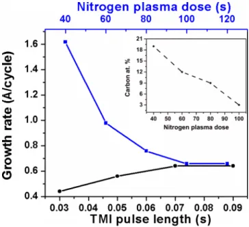
Figure1 shows the effect of indium and nitrogen precursor doses on the growth rate of InN. Initially, TMI pulse length, purge time, and growth temperature were kept constant as 0.07 s, 10 s, and 200◦C, respectively.
N2plasma exposure time was varied to investigate the effect on growth rate. After each growth
run using different N2plasma exposure time, spectroscopic ellipsometer measurement was carried
out subsequently to extract the thickness of the grown film. Growth rate was then evaluated by dividing the measured film thickness with the total number of growth cycles. Growth rate decreases progressively with increase in N2 plasma exposure time from 40 s to 100 s. It was found as
1.60 Å/cycle with 40 s of plasma exposure time which decreases to 0.64 Å/cycle under 100 s of exposure time. Growth rate remained constant as 0.64 Å/cycle with 120 s of N2plasma exposure
time, which shows that 100 s of N2plasma exposure time is enough to saturate InN growth rate. In
FIG. 1. Effect of precursor doses on growth rate at 200◦C: TMI pulse length was kept constant at 0.7 s for the N 2plasma
saturation curve, N2plasma dose was kept constant at 100 s for the TMI saturation curve. (Inset) N2plasma dose vs. carbon
order to explore the main cause of growth rate decrease, all the samples were examined by XPS and the data is presented as inset of Figure1. Films were etched using Ar+ions before taking XPS data to obtain elemental concentrations from the bulk of the films. XPS measurements revealed a decrease in carbon content of the films with increase in N2plasma exposure time. With 40 s N2plasma exposure
time, 19 at. % carbon was found in the bulk of the film. Carbon content decreases to ∼3 at. % with the increase in N2plasma exposure time to 100 s. Previously, we have demonstrated HCPA-ALD
of AlN, BN, and GaN films using the trimethylaluminum, triethylboron, and trimethylgallium, respectively together with N2/H2plasma.30–32These metal precursors belong to the organometallic
precursor family which contains methyl/ethyl groups bonded to metal atoms. Purpose of using H2plasma in addition to N2plasma was to effectively remove the carbon ligands during the film
growth. However, in the case of InN (deposited using non-optimized parameters), we had found that addition of H2 plasma with N2 plasma as second precursor resulted in InN films with poor
crystalline quality showing high level of impurities with significant voids in the films, resulting in low-density films.33This profound effect of H2plasma was attributed to plasma-related deterioration
during the growth. In that context, present results illustrate that N2-only plasma exposure time is
critical in removing the carbon containing ligands of TMI and results indicate that higher N2plasma
exposure time is necessary to obtain InN films with minimum amount of carbon incorporation. For the TMI saturation curve (Fig. 1), N2plasma dose, purge time, and growth temperature were
kept constant at 100 s, 10 s, and 200◦C, respectively. Deposition rate increased with increasing TMI dose until 0.07 s, where growth rate became saturated at ∼0.64 Å/cycle. Increasing the TMI pulse length above 0.07 s does not affect the amount of species adsorbed. Hence, reaction becomes self-terminating with sufficiently long TMI exposure and growth-per-cycle (GPC) shows a decent saturation behaviour.
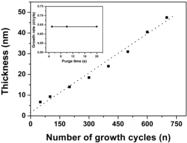
Film thickness vs. number of deposition cycles is given in Fig.2. The growth can be considered in steady regime where film thickness increases linearly with increasing number of cycles. Linear growth behaviour is an important hall mark of self-limiting ALD due to several reasons: number of cycles does not alter the number of surface reactive sites and steric hindrance of the ligands of the adsorbed species causes saturation. Steric hindrance is a well-known term in ALD where adsorbed ligands in one half reaction can shield/shadow part of the surface from being accessible to the second reactant and surface is considered “fully saturated.”29Additionally, these results show that
growth of InN begins immediately on the substrate without any incubation period. Indeed, it seems that InN growth exhibits a slight substrate-enhanced behaviour taking into account the non-zero extrapolation of the linear-fitting line.
FIG. 2. InN film thickness vs. number of deposition cycles. (Inset) Deposition rate as a function of purge time: TMI dose and N2plasma exposure time were constant at 0.7 and 100 s, respectively.
Substrate enhanced growth refers to a growth type in which number of reactive sites on the substrate is higher than on the ALD-grown material, which results in higher GPC in the beginning of the growth than at the steady regime.29
The purging time between the TMI and N2 plasma exposure steps must also be sufficiently
long. If not long enough purged, the GPC increases due to overlapping of metal and nitrogen precur-sors in gas phase, leading to non-self-limiting chemical vapor deposition (CVD)-type of growth. On the other hand, purge cycles should be short enough so that possible desorption of chemisorbed pre-cursor molecules from the substrate surface can be avoided.29The effect of purge time on deposition rate (Inset of Fig.2) was studied at 200◦C by keeping the TMI pulse length (0.07 s) and N2plasma
exposure time (100 s) at its optimized conditions. Growth rate remained constant as 0.64 Å/cycle for purge times within 5 – 20 s range, indicating that the studied range of purge time satisfies the necessary conditions for self-limiting ideal ALD. Based on this result, purging time for InN growth cycle was set to 10 s.
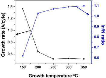
Deposition rates of InN thin films and In/N ratio has been obtained at substrate temperatures ranging from 150 to 350◦C (Fig. 3). Growth rate decreases sharply from 1.36 to 0.64 Å/cycle with the increase in growth temperature from 150 to 200◦C, respectively. With further increase in substrate temperature, GPC further decreases to ∼0.52 Å/cycle and remains saturated around this value within the temperature range of 250-350◦C. XPS measurements from bulk of InN sample grown at 150◦C reveal 25 at. % carbon which suggest the ineffective removal of carbon containing ligands (methyl groups) of TMI in the growing film possibly due to insufficient thermal energy for the completion of TMI-N2plasma reaction. These unreacted carbon containing ligands are the main
reason for the high growth rate at 150◦C.
XPS measurements were conducted on InN samples grown at different temperatures in which data was collected from the surface of the thin films. In/N ratio was computed from the surface composition of InN thin films and plotted against substrate temperature (Fig.3). At 150◦C, film is found to be N rich with In/N ratio of 0.62 while films are In rich (In/N>1) at temperatures above 200◦C. At 200◦C, film was nearly stoichiometric with In/N ratio of 1.03. A similar trend has been reported for ALE-grown InN films by Nepal et al. where they found N rich films for substrate temperatures below 180◦C and In rich films above 180◦C.25 Additionally, they reported that N
rich InN films were insulating while In rich InN films exhibited lower resistivity. Less resistive In rich films were correlated with nitrogen vacancies (VN) which is the major contributing source
of electrons in InN films. These VNwere believed to form with sufficient thermal energy only at
growth temperatures above 200◦C.25A summary of the studied growth parameters for HCPA-ALD
grown InN thin films and established values are provided in TableI.
After optimization of the main growth parameters, a 700-cycle growth of InN was carried out at 200◦C on Si(100) and double-side polished quartz for detailed material characterization at
TABLE I. Summary of studied growth parameters range and established value.
Parameters TMI pulse length (s) N2plasma exposure time (s) Purge time Growth temperature (◦C)
Studied range 0.03-0.09 40-100 5-20 150-350
Established value 0.07 100 10 200
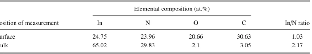
optimized conditions listed in TableI. In the rest of the article, this thin film is referenced to XPS measurement was used to analyze the elemental composition, chemical bonding states, and impurity contents of the InN film. All the spectra have been corrected for any possible charging effects, by referencing them to C1s (285.0 eV). Survey spectrum from the surface of the film shows the presence of In 3d, N 1s, C 1s, and O 1s elements. Table IIshows the chemical composition of InN film deposited on Si(100) surface, both on the as deposited surface and in the bulk. Table II illustrates that In/N ratio is closer to ∼1; which indicates that InN deposited at 200◦C possesses near-ideal stoichiometry. Surface of the film showed a highly oxidized and contaminated (21% oxygen and 31% carbon) character. High concentration of adventitious carbon and oxygen found on the surface of the film originates from post deposition atmospheric exposure. InN thin film was etched by Ar+ ions for 60 s in order to obtain XPS survey scan from the bulk of the films. Analysis of the bulk InN reveals that In/N ratio is greater than unity and indicates nitrogen deficient films.
Similar behaviour has been observed in case of ion beam deposited and reactively sputtered InN films.34,35 This observed difference in stoichiometry from surface and bulk of the films have been explained by preferential sputtering of N atoms by Ar+ions used to sputter and depth profile the film of interest. Despite the fact that Ar+ ion etching of InN does not provide information about stoichiometry from the bulk of the film due to limitation of preferential etching, it is a suitable method to estimate impurity concentration within the bulk of the film. ∼2 at. % oxygen and ∼3 at. % carbon was observed in the bulk of InN sample. Although minimized by the long N2-plasma exposure cycles, C1s signals originating from the bulk of the film indicates that
carbo-naceous ligands from indium precursor have not been removed completely during the reaction of TMI and N2 plasma. At this point, we are not sure about exact source of oxygen. However,
oxygen might come from possible sources such as impurities in plasma gases and organo-metallic precursors as well as from trapped oxygen/water vapor within the relatively thick, multi-layer coatings on the inner walls of the ALD reactor. Moreover, as films are relatively thin, molec-ular oxygen and water vapor from atmospheric ambient might diffuse into the InN thin film af-ter the deposition which depends on film characaf-teristics such as grain growth, grain boundaries, stability, defects etc. Either of the above can contribute to the oxygen incorporation in InN thin films.
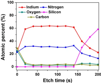
Figure4represents the compositional depth profile of InN film deposited on Si(100) substrate, which reveals the variation in atomic ratios of indium, nitrogen, carbon, oxygen, and silicon along the etching direction from the air/InN interface towards the InN/Si(100) interface. Film stoichi-ometry was disturbed after the first etching step due to the reason mentioned above. This data reveals that elemental concentration of In and N remains constant in the film along the etching direction. Both oxygen and carbon atomic concentration decays rapidly after the first etching step and becomes nearly constant after second etching step.
TABLE II. Elemental compositions and In/N ratios obtained from XPS survey spectra. Elemental composition (at.%)
Position of measurement In N O C In/N ratio
Surface 24.75 23.96 20.66 30.63 1.03
FIG. 4. Compositional depth profile of lnN thin film deposited on Si(100) at 200◦C.
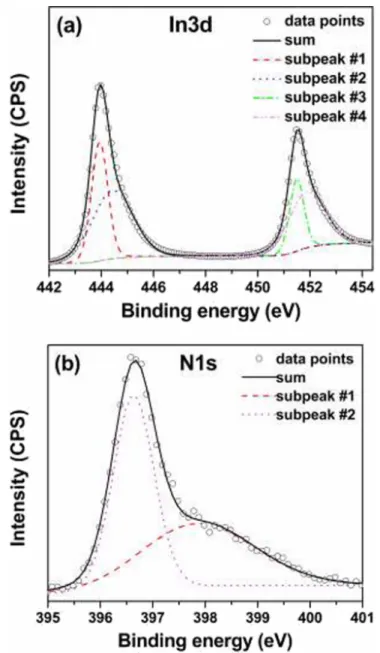
The high-resolution scans of In3d and N1s are given in Figs.5(a)and5(b), respectively, both of which refer to the bulk film (tetch= 60 s). The In3d spectrum is known to contain the In3d5/2 and
In3d3/2spin-orbit doublet (separation of 7.6 eV) and an intensity ratio of 3:2.36FWHM and
asym-metry of the peaks suggest more than one type of bonding scheme for indium and nitrogen. In3d HR spectra (Fig. 5(a)) shows In3d5/2and In3d3/2spin orbit doublet and both of these peaks have
been deconvoluted in to two Gaussians. In3d5/2 subpeak originating at 443.5 eV corresponds to
In-N bond while second subpeak at 444.42 eV is associated with In-O bonds.36,37In3d3/2peak was
deconvoluted into two subpeaks located at 451.49 and 451.88 eV, respectively. Former corresponds to In-N bond while later indicates again the presence of In-O species.16 The difference between the binding energies of the two In-3d spin orbit doublet peaks is 7.63 eV which is in agreement with previously reported values.36N1s spectra is deconvoluted with two Gaussians as shown in the
Fig.5(b). Literature reports show that N-In bond in nitrogen spectra shows feature at 396.4 eV.36
Therefore, first subpeak in N1s spectra detected at 396.8 eV can be attributed to the N-In. Bello et al. showed that the most probable formations in InN other than indium-nitride are oxynitrides.35
Any form of N-O bonding will appear in the spectra at higher binding energy with respect to the main peak (396.4 eV), i.e., the shoulder peak can be attributed to the presence of In-O bond.36,37
XPS-measured valence band spectrum of HCPA-ALD grown sample was obtained in order to extract information about electronic structure of the InN sample (Fig.6). The position of the valence band maxima has been determined from linear extrapolation of leading edge and base line (inset of Fig.6). It turns out that VBM lies at ∼1.7 eV below Fermi level for InN sample. It shows that In4d peaks are by 16.1 eV from VBM of InN. Similar values of VBM has been reported in literature for InN films grown using different techniques.37,38In our case, we have determined the band gap of InN as ∼1.9 eV by the help of optical characterization of our sample, which will be discussed later in the article. VBM position reveals that Fermi level is located fairly close to the conduction band and this in turn indicates that the grown InN layers should have n-type conductivity. However, we are not able to confirm this n type conductivity by Hall measurements due to substantial resistivity levels in the samples. Investigations on the origin of this highly resistive character are ongoing.
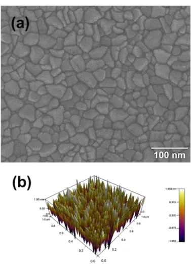
Figure 7(a) shows plane view SEM images of InN thin film deposited on Si(100) substrate using optimized parameters. Highly uniform grainy structure is apparent. Spread of grain size is relatively high as some grains grew larger than the others. Average grain size was estimated using Image J image analysis software where grains were marked using the grain boundaries as edges of the grains. Average area of grains was estimated as 3.9 × 10⁻⁴ µm2 while average diameter
was calculated as ∼22 nm. Surface morphology of the InN thin film was also examined by AFM. Figure7(b)shows the surface scan of InN thin film. Root mean square (Rms) surface roughness of the ∼48 nm thick InN film was measured as 0.98 nm from a 1µm × 1µm scan area.
FIG. 5. High resolution XPS scans of (a) In3d and (b) N1s obtained from InN thin film deposited on Si(100) at 200◦C.
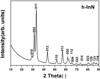
The structural properties of InN films were studied by GIXRD (Fig. 8). Measurement was performed on ∼48 nm thick InN grown on Si(100) substrate. The polycrystalline wurtzite structure of InN is clearly visible in the recorded GIXRD spectrum. The exhibited pattern was indexed by hexagonal crystal system (ICDD reference code: 00-050-1239). The lattice parameters a and c were calculated using 2θ positions of (002) and (100) reflections. Interplanar spacing (dhkl) values
of (002) and (100) planes were calculated from Bragg’s law and it was inserted into Eq. (1) to obtain the c and a axis lattice parameters. c-axis lattice parameter was deduced as 5.71 Å which is close to the value of 5.70 Å reported for fully relaxed InN films39,40 a-axis lattice parameter
was calculated to be 3.53 Å which matches well with the strain free InN films reported in the literature.39,40Recently, we have reported a and c axis lattice parameters of a ∼20 nm InN grown
using HCPA-ALD as 3.50 and 5.61 Å, respectively.23For a thick InN film (∼48 nm) reported in the present case, shift of lattice parameters towards the ideal values of stain free InN indicates the relaxation of the film. Strain reduction with the increase in thickness of the polycrystalline InN thin films has been reported in the literature as well.20
FIG. 6. Valence band spectra of InN sample deposited on Si(100) at 200◦C. Inset shows the position of spectra near valence
band maximum region.
FIG. 7. (a) SEM images of InN thin film deposited on Si(100) substrate at 200◦C, (b) Surface morphology of same sample revealed by AFM.
FIG. 8. GIXRD pattern of InN film deposited on Si(100) substrate at 200◦C.
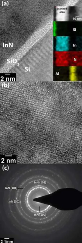
TEM experiments were carried out on InN sample grown at 200◦C on Si(100) in order to
further explore the crystal structure in detail. The sample to be examined was capped with an AlN layer to prevent any possible crystal damage of InN by high energy Ga ions of the FIB system, which is used to prepare the samples to be analysed. The average thickness of InN was measured as ∼43 nm from cross-sectional TEM measurements, which is in close agreement with the thickness data obtained from XRR measurments. Fig.9(a)shows the cross-sectional TEM image of InN sample which depicts the interface of InN with SiO2/Si. Polycrystalline structure showing
several individual crystalline domains of InN with different crystallographic orientations is visible. A ∼3 nm thick amorphous SiO2layer was observed at the InN/Si interface, which could either form
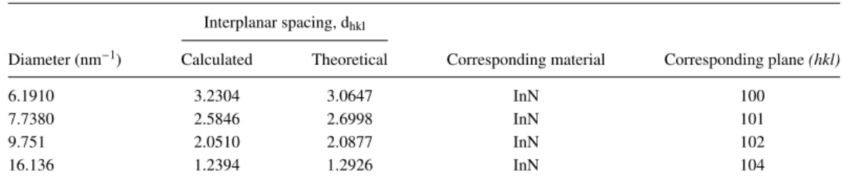
during TEM sample preparation using FIB or it was present as native oxide on the surface of Si before the InN growth. Figure9(b)shows the high resolution cross- sectional TEM image from bulk of InN thin film. It shows several crystalline subsections of InN and in each crystalline subsection, lattice fringes of InN are organized in different orientations which imply the polycrystalline struc-ture of InN. Inset of Fig.9(a)shows EDX elemental maps of In, N, Al and Si obtained from the AlN-capped InN thin film sample deposited on Si(100) at 200◦C. A cross sectional portion of the film is selected and elemental distribution is clarified by exposing the electron beam point by point over the selected portion of interest. Si, In, N, and Al show strong contrast in the colorized maps and they are represented by different colours which show their presence within the scanned area. Presence of Al originates from AlN which was used as capped layer for TEM sample preparation. Interface of AlN and InN is distinct and distribution of In and N is fairly uniform in the scanned InN region. Figure 9(c)shows SAED pattern of the same InN sample. Polycrystalline diffraction rings of InN can be seen from this pattern. The interplanar spacing (dhkl) values were calculated
from the diffraction rings which have been shown in TableIII. The diffraction rings are indexed as (100), (101), (102), and (104) reflections of hexagonal structure of polycrystalline InN, which are supported by GIXRD results (ICDD reference code: 00-050-1239).
Refractive index and extinction coefficient of InN film deposited at 200◦C are shown in
Fig.10(a). Refractive index, which is 2.66 at 650 nm, decreases to 2.09 at 1500 nm. These values are in good agreement with the reported values for polycrystalline hexagonal InN thin films.41 Previously, we had reported refractive index value of 2.55 at 650 nm for a ∼20 nm InN thin film grown by HCPA-ALD at the same substrate temperature but non-optimized growth conditions.33 This shows that, with the increase in thickness of InN from 20 to 48 nm, refractive index increased from 2.55 to 2.66 at 650 nm. This improvement might be attributed to film densification with the increase in thickness of the film. Extinction coefficient (k) of InN film, which is ∼0.51 at 600 nm, decreases rapidly within the wavelength range of 600–800 nm. At longer wavelengths, k value further decreases and reaches rather insignificant level.
FIG. 9. (a) Cross-sectional TEM image of AlN capped InN film showing the interface of InN and SiO2/Si deposited at 200◦C on Si(100) substrate. (Inset) Colorized elemental map of same sample. (b) Cross-sectional TEM image of same InN sample. (c) SAED pattern of the same sample.
Figure 10(b) shows (αhν)2 vs. hν plot, which is obtained from spectroscopic ellipsometer
measurement and related data analysis as explained in experimental section. Straight line segment of the plot was extrapolated to abscissa which reveals the optical band gap of the material as ∼1.9 eV. Inset of Fig.10(b) shows optical transmission spectra of InN sample grown on double
TABLE III. SAED pattern analysis of InN thin film deposited on Si(100) substrate at 200◦C: comparison between measured
and theoretical values of interplanar spacing (dhkl) with corresponding crystallographic planes.
Interplanar spacing, dhkl
Diameter (nm−1) Calculated Theoretical Corresponding material Corresponding plane (hkl)
6.1910 3.2304 3.0647 InN 100
7.7380 2.5846 2.6998 InN 101
9.751 2.0510 2.0877 InN 102
16.136 1.2394 1.2926 InN 104
side polished quartz substrate. Transmission values did not saturate for InN sample, probably due to the high defect density present within the films.33InN thin film exhibits 40-50% transmission in
the visible regime, which approaches up to 60-70% in the NIR regime. There is a huge controversy in literature for experimental InN thin film band gap values and origin of the observed InN band gap variations between 0.6 and 2.3 eV is not very well understood. This significant discrepancy has been ascribed to several reasons and among them the most prominent ones are the Burstein-Moss shift, defect levels, stoichiometry, and impurity levels. 0.7 eV has been dominantly reported as the
FIG. 10. (a) Optical constants (refractive index and extinction coefficient) of InN thin film deposited on Si(100) at 200◦C,
(b) Absorption spectrum of same InN sample deposited on Si(100). (Inset) Optical transmission spectrum of the InN film deposited on double-side polished quartz.
optical band gap for MBE-grown single-crystalline InN which became most popular and widely accepted, however there are some doubts as well that this value might originate from a 0.7 eV trapping level. Energy band gap less than 1 eV is mostly obtained from single crystalline InN films, while larger band gap values are reported mostly for polycrystalline InN thin films. From the view point of narrow band gap, larger band gap (1.9 eV) might be due to formation of oxynitrides which have considerable larger band gap than InN. Polycrystalline films can contain a significant level of oxygen incorporation at their grain boundaries which might be the cause of higher band gap in polycrystalline films. There is a growing evidence of 1.1-1.5 eV band gap for InN films in the literature as well. In view of numerous different reports, further investigation will be helpful to reach conclusive evidence for establishing a unanimous InN band gap.1,3,42
IV. SUMMARY AND CONCLUSIONS
In this study, we have deposited crystalline InN thin films on Si(100) with self-limiting HCPA-ALD at temperatures as low as 200◦C. Growth rate decreased from 1.60 to 0.64 Å/cycle with increase in N2 plasma exposure time from 40 s to 100 s. This higher growth rate with 40 s of N2
plasma exposure was attributed to presence of carbon in InN films which was originating from the partial removal of carbon containing TMI ligands. Longer N2plasma exposure time helped in
removing carbonaceous ligands more effectively, which decreased the growth rate of InN. Growth rate at 200◦C was saturated as 0.64 Å/cycle for TMI dose starting from 0.07 s. Film thickness increased linearly with number of cycles and no nucleation delay was observed. Purge time had no effect on growth rate in the studied range (5-20 s). InN film deposited at 200◦C was polycrystalline
with hexagonal wurtzite structure as determined by GIXRD. XPS survey scans and high resolution XPS measurements confirmed the successful growth of stoichiometric InN films with relatively low impurity content. AFM revealed smooth films with Rms surface roughness of 0.98 nm while XRR reveals film density of 6.30 g/cm3. TEM and SAED measurements verified the polycrystalline
structure of InN thin films and EDX elemental mapping revealed uniform distribution of indium and nitrogen along the scanned area of the InN film. Film exhibited refractive index of 2.66 at 650 nm and optical band edge at 1.9 eV. The results of this study might be further improved to achieve device-layer quality InN films at low substrate temperatures.
ACKNOWLEDGMENTS
Authors would like to acknowledge M. Guler from UNAM for TEM sample preparation and HR-TEM measurements. A. H. acknowledge Higher Education Commission of Pakistan (HEC) for Human resource development (HRD) fellowship for MS leading to PhD. N. B. acknowledge the financial support from TUBITAK (Project # 112M004, 112M482, and 214M015).
1A. G. Bhuiyan, A. Hashimoto, and A. Yamamoto,J. Appl. Phys94, 2779–2808 (2003).
2E. Bellotti, B. K. Doshi, K. F. Brennan, J. D. Albrecht, and P. P. Ruden,J. Appl. Phys.85, 916–923 (1999). 3K. S. A. Butcher and T. L. Tansley,Superlattices Microstruct.38, 1–37 (2005).
4V. Y. Davydov, A. A. Klochikhin, V. V. Emtsev, S. V. Ivanov, V. V. Vekshin, F. Bechstedt, J. Furthmuller, H. Harima, A. V.
Mudryi, A. Hashimoto et al.,Phys. Status Solidi B230, R4–R6 (2002).
5V. Y. Davydov, A. A. Klochikhin, V. V. Emtsev, S. V. Ivanov, V. V. Vekshin, F. Bechstedt, J. Furthmüller, H. Harima, A. V.
Mudryi, A. Hashimoto et al.,Phys. Status Solidi B234, 787–795 (2002).
6S. Strite and H. Morkoc,J. Vac. Sci. Technol. B10, 1237–1266 (1992). 7O. Ambacher,J. Phys. D. Appl. Phys.31, 2653–2710 (1998).
8J. Kamimura, K. Kishino, and A. Kikuchi,J. Appl. Phys117, 084314 (2015).
9J. Sakaguchi, T. Araki, T. Fujishima, E. Matioli, T. Palacios, and Y. Nanishi,Jpn. J. Appl. Phys.52, 08JD06 (2013). 10J. J. Williams, T. L. Williamson, M. A. Hoffbauer, Y. Wei, N. N. Faleev, and C. Honsberg,Phys. Status Solidi C.11, 577–580
(2014).
11T. Kehagias, G. P. Dimitrakopulos, A. O. Ajagunna, T. Koukoula, K. Tsagaraki, A. Adikimenakis, P. Komninou, and A.
Georgakilas,J. Appl. Phys.114, 163519 (2013).
12G. R. Mutta, T. Brazzini, L. Méchin, B. Guillet, J.-M Routoure, J.-L. Doualan, J. Grandal, M. D. C. Sabido Siller, F. Calle,
and P. Ruterana,Semicond. Sci. Technol29, 095010 (2014).
13Y. Nanishi, Y. Saito, and T. Yamaguchi,Japanese J. Appl. Physics42, 2549–2559 (2003).
15M. Alevli, N. Gungor, S. Alkis, C. Ozgit-Akgun, I. Donmez, A. K. Okyay, S. Gamage, I. Senevirathna, N. Dietz, and N.
Biyikli,Phys. Status Solidi C12, 423–429 (2015).
16M. K. Indika Senevirathna, S. Gamage, R. Atalay, A. R. Acharya, A. G. Unil Perera, N. Dietz, M. Buegler, A. Hoffmann,
L. Su, A. Melton et al.,J. Vac. Sci. Technol. A30, 031511 (2012).
17M. Amirhoseiny, S. S. Ng, and Z. Hassan,Mater. Sci. Semicond. Process.35, 216–221 (2015). 18T. Sasaoka, M. Mori, T. Miyazaki, and S. Adachi,J. Appl. Phys.108, 063538 (2010). 19M. Sparvoli, R. D. Mansano, and J. F. D. Chubaci,Phys. Status Solidi210, 1606–1611 (2013).
20M. V. S. Da Silva, D. G. F. David, I. Pepe, A. Ferreira da Silva, J. S. de Almeida, A. L. Gazoto, A. O. dos Santos, L. P.
Cardoso, E. A. Meneses, D. L. Graybill et al.,Thin Solid Films520, 4848–4852 (2012).
21K. S. A. Butcher, D. Alexandrov, P. Terziyska, V. Georgiev, D. Georgieva, and P. W. Binsted,Phys. Status Solidi A209,
41–44 (2012).
22M. A. Hafez and H. E. Elsayed-Ali,J. Vac. Sci. Technol. A27, 696–699 (2009).
23A. Haider, S. Kizir, C. Ozgit-Akgun, E. Goldenberg, S. A. Leghari, A. K. Okyay, and N. Biyikli,J. Mater. Chem. C3,
9620–9630 (2015).
24A. Haider, S. Kizir, C. Ozgit-Akgun, A. K. Okyay, and N. Biyikli,J. Vac. Sci. Technol. A34, 01A123 (2016).
25N. Nepal, N. A. Mahadik, L. O. Nyakiti, S. B. Qadri, M. J. Mehl, J. K. Hite, and C. R. Eddy,Cryst. Growth Des.13,
1485–1490 (2013).
26S.-Y. Kuo, W.-C. Chen, C.-N. Hsiao, and F.-I. Lai,J. Cryst. Growth310, 4963–4967 (2008). 27Y. Bu, L. Ma, and M. C. Lin,J. Vac. Sci. Technol. A11, 2931–2937 (1993).
28H. B. Profijt, S. E. Potts, M. C. M. Van De Sanden, and W. M. M. Kessels,J. Vac. Sci. Technol. A29, 050801 (2011). 29L. R. Puurunen,J. Appl. Phys.97, 121301 (2005).
30C. Ozgit-Akgun, E. Goldenberg, A. K. Okyay, and N. Biyikli,J. Mater. Chem. C2, 2123–2136 (2014). 31A. Haider, C. Ozgit-Akgun, F. Kayaci, A. K. Okyay, T. Uyar, and N. Biyikli,Apl Mater.2, 096109 (2014). 32A. Haider, C. Ozgit-Akgun, E. Goldenberg, A. K. Okyay, and N. Biyikli,J. Am. Ceram. Soc97, 4052–4059 (2014). 33C. Ozgit-Akgun, E. Goldenberg, S. Bolat, B. Tekcan, F. Kayaci, T. Uyar, A. K. Okyay, and N. Biyikli,Phys. Status Solidi
C12, 394–398 (2015).
34S. Kumar, L. Mo, M. Motlan, and T. L. Tansley,Jpn. J. Appl. Phys.35, 2261–2265 (1996). 35I. Bello, W. M. Lau, R. P. W. Lawson, and K. K. Foo,J. Vac. Sci. Technol. A10, 1642–1646 (1992). 36I. J. Lee and C. Yu, J. Korean Phys.Soc 49, 2176–2179 (2006).
37V. Lebedev, V. Cimalla, J. Pezoldt, M. Himmerlich, S. Krischok, J. A. Schaefer, O. Ambacher, F. M. Morales, J. G. Lozano,
and D. González,J. Appl. Phys100, 094902 (2006).
38C. F. Shih, N. C. Chen, and C. Y. Tseng,Thin Solid Films516, 5016–5019 (2008). 39M. A. Moram and M. E. Vickers,Reports Prog. Phys72, 036502 (2009).
40M. F. Wu, S. Q. Zhou, A. Vantomme, Y. Huang, H. Wang, and H. Yang,J. Vac. Sci. Technol. A24, 275–279 (2006). 41L. F. Jiang, W. Z. Shen, H. F. Yang, H. Ogawa, and Q. X. Guo,Appl. Phys. A Mater. Sci. Process.78, 89–93 (2004). 42V. Y. Davydov, A. A. Klochikhin, R. P. Seisyan, V. V. Emtsev, S. V. Ivanov, F. Bechstedt, J. Furthmüller, H. Harima, A. V.