Nonlinear Laser Lithography for Photonic Design of Si Solar Cells
I. Pavlov1, T. Çolakoğlu2, F. Es2, A. Bek², R. Turan2, I Gnilitskyi3, and O.Ilday11. Department of Physics, Bilkent University, 06800 Ankara, Turkey
2. Center for Solar Energy Research and Application, Middle East Technical University… Ankara, Turkey
3. Department of Sciences and Methods for Engineering , University of Modena and Reggio Emilia,via Amendola, 42020, Reggio Emilia, Italy
Nowadays Si-based solar cell (SC) remains the main source of solar energy in the world due to low cost of material and relatively simple, industrially acceptable technology. Despite of significant progress on increasing efficiency of these devices (the best laboratory samples demonstrated efficiency as much as 43.5%), for most of industrially manufactured SC`s the efficiency remains in the range of 10-18% [1]. A promising way to minimize thermodynamic losses for high efficiency Si-based photovoltaic devices, is photonic design of the device surfaces. The last one causes light trapping into the device, due to light interaction with micro- nano-structured surfaces, thus increasing effective light path interaction. However, the most of proposed methods for Si surface modification do not match industrial production requirements: such as fast manufacturing, environmental issues, and low cost per watt for final devices.
Recently, we developed a new method, Nonlinear Laser Lithography (NLL) [2], for laser-induced periodic surface structuring, which allows nanostructuring of indefinitely large areas of many materials by excellent periodicity and uniformity. Given that NLL is a low-cost, single-step and high-speed technique, there is significant potential for applications.
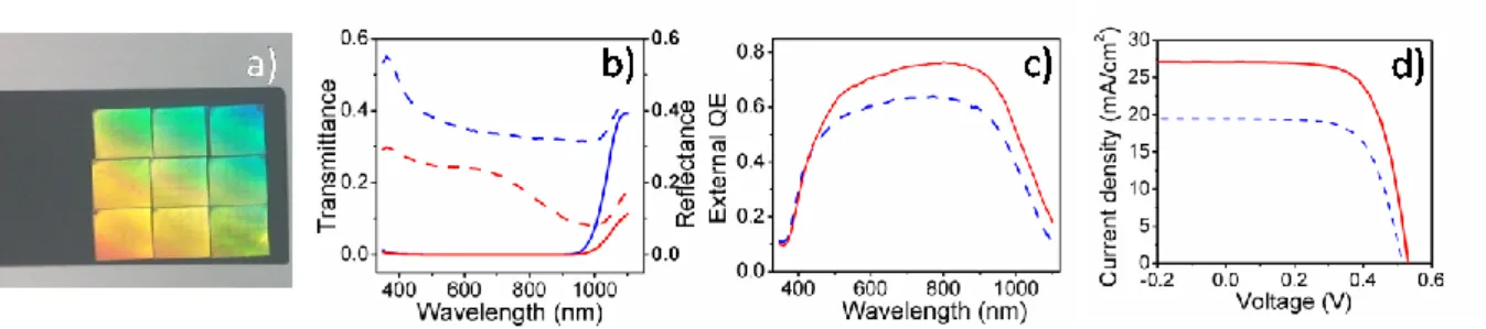
In present work we report the creation of photonic structure on Si-based SC by using NLL technique. As a laser source we used home-made 1 MHz femtosecond laser system, which can generate up to 1 μJ of pulse energy with ~120 fs of pulse duration. The laser beam was focused on Si surface and raster scanned with galvo-scanner to obtain area 1x1 cm2. Much larger areas were obtained by translating the sample with translation stage under galvo-scanner. In our work the structured area was 3x3 cm2. The macroscopic image of structured surface is presented in fig.1 (a). From SEM analysis the period of the structure is found to be around 800 nm.
The sample was single crystalline p-doped Si wafer, with 4 Ω·cm resistivity and thickness – 300 μm. The SC`s were produced on the same Si wafer for both structured and unstructured areas under the same production conditions. The p-n junction was formed by phosphorous diffusion in doping furnace. The final step was back and front surface metallization in order to form electrical contacts.
Transmission and reflection graphs for structured and unstructured areas are present in fig.1 (b). The reflection graphs show decreasing reflectivity of structured area, especially in the region of 800 nm and longer, which clearly demonstrates photonic effects on the surface, where the period of structure become comparable with the wavelength of the light. As a result, the external quantum efficiency (EQE) of processed area is higher (fig. 1 (d)). For the range between 400 nm to 800 nm the relative increase in EQE is ~20%, while for the range 800 nm and longer it is more than 30%. From the current-voltage curve (fig. 1 (d)), the open circuit voltage (VOC) and short circuit current (JSC) density for unstructured SC is 0.516 V and 19.44 mA/cm
2
, respectively. For structured one VOC and JSC are 0.532 V and 27.09 mA/cm2. Conversion efficiency and fill factor for unstructured
SC 6.6% and 65.7% respectively. For structured SC efficiency increases to 9.6% with fill factor value of 66.5%.
In conclusion, we propose and experimentally demonstrate the recently invented NLL technique as a low-cost, high-speed, step technique for photonic design of Si-based solar cells. For high-resistive single-crystalline Si, relative increase of conversion efficiency is found to be 45%. We expect this technique to be successfully applicable to solar cells, as well as for other photovoltaic and sensing devices.
References
1 A. Polman and H. A. Atwater, "Photonic design principles for ultrahigh-efficiency photovoltaics," Nature Materials 11, 174 (2012). 2 B. Öktem, I. Pavlov, S. Ilday, H. Kalaycıoğlu, A. Rybak, S. Yavaş, M. Erdoğan and F. O. Ilday, "Nonlinear laser lithography for indefinitely large-area nanostructuring with femtosecond pulses," Nature Photonics 7, 897 (2013).
Fig. 1 (a) – Macrophotogram of 3x3 cm2 structured area. (b) – transmittance (solid) and reflectance (dashed) curves for unstructured (blue), and structured (red) areas. (c) – EQE graphs for unstructured (blue) and structured (red) solar cell. (d) – I-V graph for unstructured (blue) and structured (red) solar cell.