Fabrication and characterization of liquid metal-based micro-electromechanical DC-contact switch for RF applications
4
0
0
Tam metin
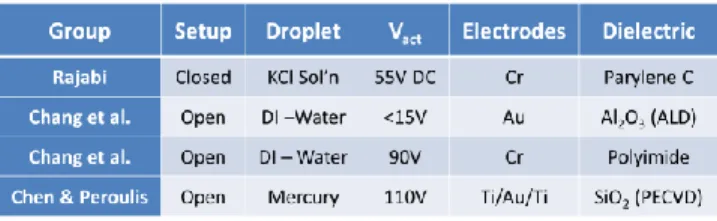
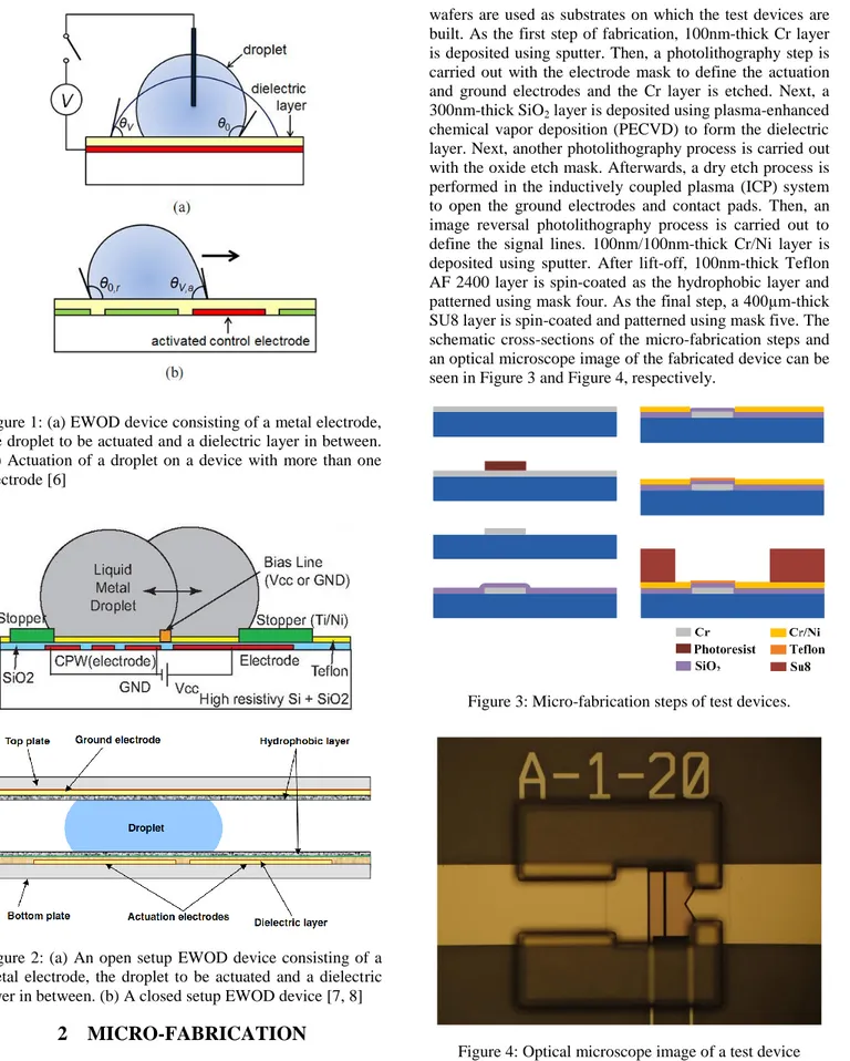
(2) wafers are used as substrates on which the test devices are built. As the first step of fabrication, 100nm-thick Cr layer is deposited using sputter. Then, a photolithography step is carried out with the electrode mask to define the actuation and ground electrodes and the Cr layer is etched. Next, a 300nm-thick SiO2 layer is deposited using plasma-enhanced chemical vapor deposition (PECVD) to form the dielectric layer. Next, another photolithography process is carried out with the oxide etch mask. Afterwards, a dry etch process is performed in the inductively coupled plasma (ICP) system to open the ground electrodes and contact pads. Then, an image reversal photolithography process is carried out to define the signal lines. 100nm/100nm-thick Cr/Ni layer is deposited using sputter. After lift-off, 100nm-thick Teflon AF 2400 layer is spin-coated as the hydrophobic layer and patterned using mask four. As the final step, a 400µm-thick SU8 layer is spin-coated and patterned using mask five. The schematic cross-sections of the micro-fabrication steps and an optical microscope image of the fabricated device can be seen in Figure 3 and Figure 4, respectively. Figure 1: (a) EWOD device consisting of a metal electrode, the droplet to be actuated and a dielectric layer in between. (b) Actuation of a droplet on a device with more than one electrode [6]. Figure 3: Micro-fabrication steps of test devices.. Figure 2: (a) An open setup EWOD device consisting of a metal electrode, the droplet to be actuated and a dielectric layer in between. (b) A closed setup EWOD device [7, 8]. 2 MICRO-FABRICATION Figure 4: Optical microscope image of a test device The fabrication of the devices used in this work consisted of a five-mask micro-fabrication process. Quartz. 162. NSTI-Nanotech 2012, www.nsti.org, ISBN 978-1-4665-6275-2 Vol. 2, 2012.
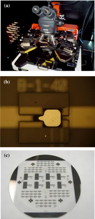
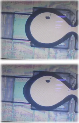
(3) 3. RESULTS AND DISCUSSION. Characterization of the test devices involved visual inspection with optical microscope and FEI-brand NanoSEM, contact angle measurements of DI-water on hydrophobic surfaces using Dataphysis OCA 30 and voltage actuation experiments under a Cascade-Microtech electrical probe station connected to a Keithley 4200-SCS parameter analyzer (Fig. 5).. (a). (b). Figure 6 shows the contact angle measurements of the hydrophobic layer with DI-water: the contact angle on Teflon AF 2400 is 130.1°. The aim of Teflon coating is to get the optimum initial contact angle during droplet actuation. During actuation experiments, two different metallic liquids have been used: Eutectic Gallium Indium (EGaIn) and Gallium Indium Tin alloy (Galinstan). With the application of 80-100V across the actuation electrode and the ground electrode, the metallic liquid droplets were observed to be actuated (Fig. 7).. Figure 6: Contact-angle measurement of Teflon-coated surface We have observed significant differences in the actuation behavior of the metal droplets with the application of AC and DC voltages. Actuation experiments in closedpack microfluidic channels were also successful with slightly higher actuation voltages. We attribute this result to the partial adhesion of liquid-metal droplets to the SU-8 walls, especially at the corners. The effect of dielectric layer thickness on the actuation voltage was also studied. Thinner dielectric layers resulted in lower actuation voltages as low as 30 V. Results of this study may be potentially used in non-toxic alternative RF-switching applications. RF-measurements of the microfluidic switches are currently in progress.. (c). Figure 5: (a) The experimental setup used in this work: a probe station connected to a parameter analyzer; (b) A test device with a positioned metallic droplet; (c) a fabricated 4inch quartz wafer with many test devices. NSTI-Nanotech 2012, www.nsti.org, ISBN 978-1-4665-6275-2 Vol. 2, 2012. 163.
(4) Grant (IRG) for funding NEMSmart (PIRG05-GA-2009249196) project.. REFERENCES [1] Chang, Choi, Han and Pak, Microfluid Nanofluid (2010) 8:269-273 [2] Wu et al., Journal of Micromechanics and Microengineering, Vol. 20, pp. 8, 2012 [3] Rajabi and Dolatabadi, Colloids and Surfaces A: Physicochem. Eng. Aspects 365 (2010) 230-236 [4] Shen, Edwards and Kim. Journal of Microelectromechanical Systems, Vol 15, No. 4, August 2006 [5] Dickey, Chiechi, Larsen, Weiss, Weitz and Whitesides, Adv. Funct. Mater. 2008. 18, 1097-1104 [6] Chang et al., Journal of Electrical Engineering & Technology Vol. 6, No. 3, pp. 402~407, 2011 [7] Sen and Kim, IEEE Transactions on Industrial Electronics, Vol. 56, NO. 4, 2009 [8] Kumari et al., Journal of Micromechanics and Microengineering, Vol. 18, pp. 10, 2008. Figure 7: Top: Test device before actuation; Bottom: Actuation of the droplet with an actuation voltage of 100V.. 4. CONCLUSIONS. In this work, we demonstrate that room-temperature liquid metal alloy droplets of Eutectic Gallium Indium (EGaIn) and Gallium Indium Tin alloy (Galinstan) can be actuated using electro-wetting-on-dielectric (EWOD) effect. With the application of 80-100V across the actuation electrode and the ground electrode, the metallic liquid droplets were observed to be actuated. Actuation experiments with and without thick SU-8 wall structures, different dielectric thicknesses, different droplet materials (EGaIn and Galinstan) and different droplet sizes, different dielectric materials including SiO2, Al2O3, and HfO2 were carried out, as well as DC and AC actuation experiments. The initial results are promising and with a systematic experimental optimization the micro-electromechanical droplet-based switches might provide an alternative technology for RF-switching applications.. ACKNOWLEDGEMENT State Planning Organization (DPT) of Turkey is acknowledged for the support of UNAM-Institute of Materials Science and Nanotechnology. Dr. Biyikli acknowledges Marie Curie International Reintegration. 164. NSTI-Nanotech 2012, www.nsti.org, ISBN 978-1-4665-6275-2 Vol. 2, 2012.
(5)
Şekil
Benzer Belgeler
Figure 3 shows the region of the photoelectron spectra where Cl, S 2s and 2p peaks and Cd and In 4d peaks are present for the various CdS coated glasses obtained under different
After admittance of Haga with the Sultan and just before the granting of the Dutch capitulations, Halil Paşa sent a letter to the States General and Prince Maurice
For the six specific problems introduced at the outset, our results compare remarkably well with what exists in the literature at present (this is particularly true for AWCTV). The
Çalışma ile Türkiye’de 2000 yılı sonrası belirli dönemlerde değişen teşvik mevzuatıyla, 2009 yılına kadar uygulanan teşvik araçlarının sektörel
The final explanation can be related cultural barriers or discrimination, which makes females disadvantageous in the labor market and reduces the likelihood of getting a
The program is observed to be based upon three main components: (i) austerity of public expenditures subject to specific targets for non-interest fiscal surpluses; (ii) a
The practical importance of Proposition 4 is that it sets an upper bound on the performance improvement that can be obtained by using the optimal single-threshold detector instead
Plasmonic interactions can also be harnessed by using the active feedback from the interaction between the optical tweezer beam and the trapped particle.. It is possible to
