High-speed visible-blind GaN-based indium–tin–oxide Schottky photodiodes
Necmi Biyikli, Tolga Kartaloglu, Orhan Aytur, Ibrahim Kimukin, and Ekmel Ozbay
Citation: Appl. Phys. Lett. 79, 2838 (2001); doi: 10.1063/1.1412592 View online: http://dx.doi.org/10.1063/1.1412592
View Table of Contents: http://aip.scitation.org/toc/apl/79/17
Published by the American Institute of Physics
Articles you may be interested in
High-speed solar-blind photodetectors with indium-tin-oxide Schottky contacts
Applied Physics Letters 82, 2344 (2003); 10.1063/1.1566459
High-responsivity photoconductive ultraviolet sensors based on insulating single-crystal GaN epilayers
Applied Physics Letters 60, 2917 (1998); 10.1063/1.106819
Effects of thermal annealing on the indium tin oxide Schottky contacts of GaN
Applied Physics Letters 72, 3317 (1998); 10.1063/1.121636
Schottky barrier detectors on GaN for visible–blind ultraviolet detection
Applied Physics Letters 70, 2277 (1998); 10.1063/1.118837
Effect of electron blocking layer on efficiency droop in InGaN/GaN multiple quantum well light-emitting diodes
Applied Physics Letters 94, 231123 (2009); 10.1063/1.3153508
Origin of efficiency droop in GaN-based light-emitting diodes
High-speed visible-blind GaN-based indium–tin–oxide
Schottky photodiodes
Necmi Biyikli,a)Tolga Kartaloglu, and Orhan Aytur
Department of Electrical and Electronics Engineering, Bilkent University, Bilkent Ankara 06533, Turkey Ibrahim Kimukin and Ekmel Ozbay
Department of Physics, Bilkent University, Bilkent Ankara 06533, Turkey 共Received 5 July 2001; accepted for publication 13 August 2001兲
We have fabricated GaN-based high-speed ultraviolet Schottky photodiodes using indium–tin– oxide共ITO兲 Schottky contacts. Before device fabrication, the optical transparency of thin ITO films in the visible-blind spectrum was characterized via transmission and reflection measurements. The devices were fabricated on n⫺/n⫹ GaN epitaxial layers using a microwave compatible fabrication process. Our ITO Schottky photodiode samples exhibited a maximum quantum efficiency of 47% around 325 nm. Time-based pulse-response measurements were done at 359 nm. The fabricated devices exhibited a rise time of 13 ps and a pulse width of 60 ps. © 2001 American Institute of
Physics. 关DOI: 10.1063/1.1412592兴
Visible/solar-blind photodetectors are essential compo-nents for a number of applications including missile-launching detection, flame sensing, ultraviolet 共UV兲 radia-tion monitoring, and secure space-to-space communicaradia-tions. Due to their direct band gap, sharp band-edge cut-off char-acteristics, and good electrical properties, AlxGa1⫺xN/GaN
is the most promising material system for high-performance UV photodetectors.1With the advancing growth technology of epitaxial AlxGa1⫺xN/GaN layers, AlxGa1⫺xN/GaN-based
visible/solar-blind photodiodes共PDs兲 with excellent detector performances have been demonstrated by several research groups.2–11 The difficulty of p-type doping of AlxGa1⫺xN
layers, ease of fabrication, and better high-frequency charac-teristics makes Schottky PDs attractive for high-performance UV photodetection. AlxGa1⫺xN-based Schottky PDs with
different types of thin semitransparent metal contacts have been fabricated successfully. Responsivities as high as 0.18 A/W 共Ref. 12兲 and 3 dB bandwidths of 16 GHz 共Ref. 13兲 were obtained with GaN-based Pd Schottky and Pt metal– semiconductor–metal共MSM兲 type PDs, respectively.
Due to the very high absorptance of GaN layers, the efficiency performance of GaN Schottky PDs with suffi-ciently thick 共⬎200 nm兲 absorption layers is limited by the transmittance of the Schottky contact layer.14 Semitranspar-ent Schottky metal layers are highly absorptive and reflec-tive, and have huge surface roughnesses, all reducing the quantum efficiency of the devices. Indium–tin–oxide共ITO兲, which is known as a transparent conductor, has been demon-strated as a transparent Schottky-contact material for PDs operating in the visible15,16 and infrared spectrum.17 Both high-quality ITO ohmic18 and Schottky19 contacts to GaN layers were reported. However, to our knowledge visible-blind GaN-based PDs using ITO Schottky contacts were not reported before. In this letter, we report a demonstration of visible-blind ITO Schottky PDs with RC limited pulse re-sponses. We also compare the performance of our ITO
Schottky PDs with Au Schottky PDs fabricated on the same wafer.
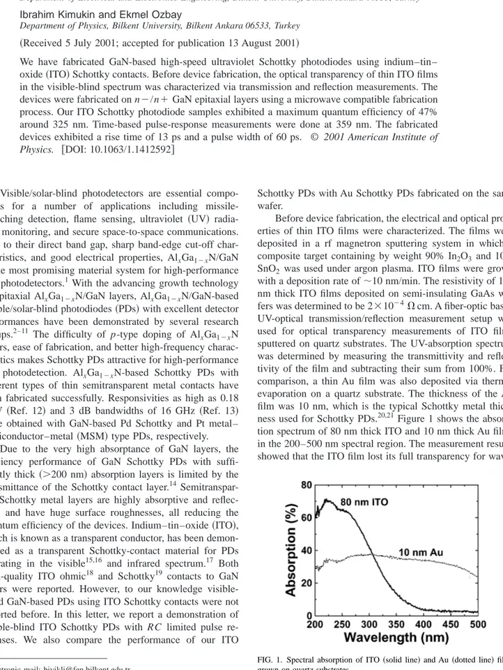
Before device fabrication, the electrical and optical prop-erties of thin ITO films were characterized. The films were deposited in a rf magnetron sputtering system in which a composite target containing by weight 90% In2O3 and 10% SnO2 was used under argon plasma. ITO films were grown with a deposition rate of⬃10 nm/min. The resistivity of 100 nm thick ITO films deposited on semi-insulating GaAs wa-fers was determined to be 2⫻10⫺4⍀ cm. A fiber-optic based UV-optical transmission/reflection measurement setup was used for optical transparency measurements of ITO films sputtered on quartz substrates. The UV-absorption spectrum was determined by measuring the transmittivity and reflec-tivity of the film and subtracting their sum from 100%. For comparison, a thin Au film was also deposited via thermal evaporation on a quartz substrate. The thickness of the Au film was 10 nm, which is the typical Schottky metal thick-ness used for Schottky PDs.20,21Figure 1 shows the absorp-tion spectrum of 80 nm thick ITO and 10 nm thick Au films in the 200–500 nm spectral region. The measurement results showed that the ITO film lost its full transparency for
wave-a兲Electronic mail: [email protected] FIG. 1. Spectral absorption of ITOgrown on quartz substrates. 共solid line兲 and Au 共dotted line兲 films
APPLIED PHYSICS LETTERS VOLUME 79, NUMBER 17 22 OCTOBER 2001
2838
lengths shorter than 400 nm. However, the 80 nm thick ITO film still exhibited lower absorption than the 10 nm thick semitransparent Au film for ⬎310 nm. For wavelengths near the band gap edge of GaN 共⬃360 nm兲, the ITO film absorbed less than 10% of the incident radiation. These re-sults convinced us that ITO films could be used as low-loss Schottky contacts on GaN layers for visible-blind PD opera-tion.
The epitaxial GaN layers of our Schottky PD wafer were grown on a sapphire substrate using metalorganic chemical vapor deposition共MOCVD兲. First an undoped GaN layer of 1.5 m thickness was grown which was used as the mesa isolation layer. This was followed by the deposition of a 1.0 m thick, highly doped (n⫹⫽2⫻1018 cm⫺3) GaN ohmic contact layer. The growth process was completed with a 0.3 m thick, lightly doped (n⫽1⫻1017 cm⫺3) active layer.
The samples were fabricated by a four-step microwave-compatible fabrication process in a class-100 clean room en-vironment. First, the ohmic contacts were defined via reac-tive ion etching 共RIE兲 under CCl2F2 plasma, a 20 sccm gas
flow rate, and 100 W rf power. With an etch rate of ⬃28 nm/min, an ohmic etch of ⬃0.6 m was completed in 22 min. Afterwards Ti/Al contacts were deposited using thermal evaporation and a standard lift-off process. The contacts were annealed at 450 °C for 45 s in a rapid thermal annealing 共RTA兲 system. Mesa structures of the devices were formed via the same RIE process by etching all the layers down to the undoped mesa isolation layer. The third step was the deposition of the Schottky contact material, where 80 nm thick ITO and 10 nm thick Au films were sputtered and evaporated, respectively, on two separate samples. The ITO films were etched to define the contact regions using dilute HF:H2O solution, whereas the Au films were lifted off in
acetone. Finally, a⬃0.7 m thick Ti/Au interconnect metal was deposited and lifted off to connect the Schottky layers to coplanar waveguide transmission line pads. The resulting GaN ITO Schottky PDs had breakdown voltages around 5 V and turn-on voltages around 0.8 V. The ITO Schottky devices displayed leakage currents larger than 1 A at 1 V reverse bias for 100 m diam devices, mainly due to the low ITO–GaN Schottky barrier height, which was measured as 0.59 eV by forward current–voltage (I – V) measurements. Au Schottky detectors had better I – V characteristics than ITO Schottky devices. The Au–GaN Schottky barrier height was measured as 0.75 eV, which led to breakdown voltages larger than 10 V. Dark currents smaller than 1 nA at 1 V reverse bias for 150m diameter devices were obtained. The turn-on voltages were around 0.3 V for Au Schottky PDs. The ideality factors were 1.15 and 1.19 for the ITO Schottky and Au Schottky samples, respectively.
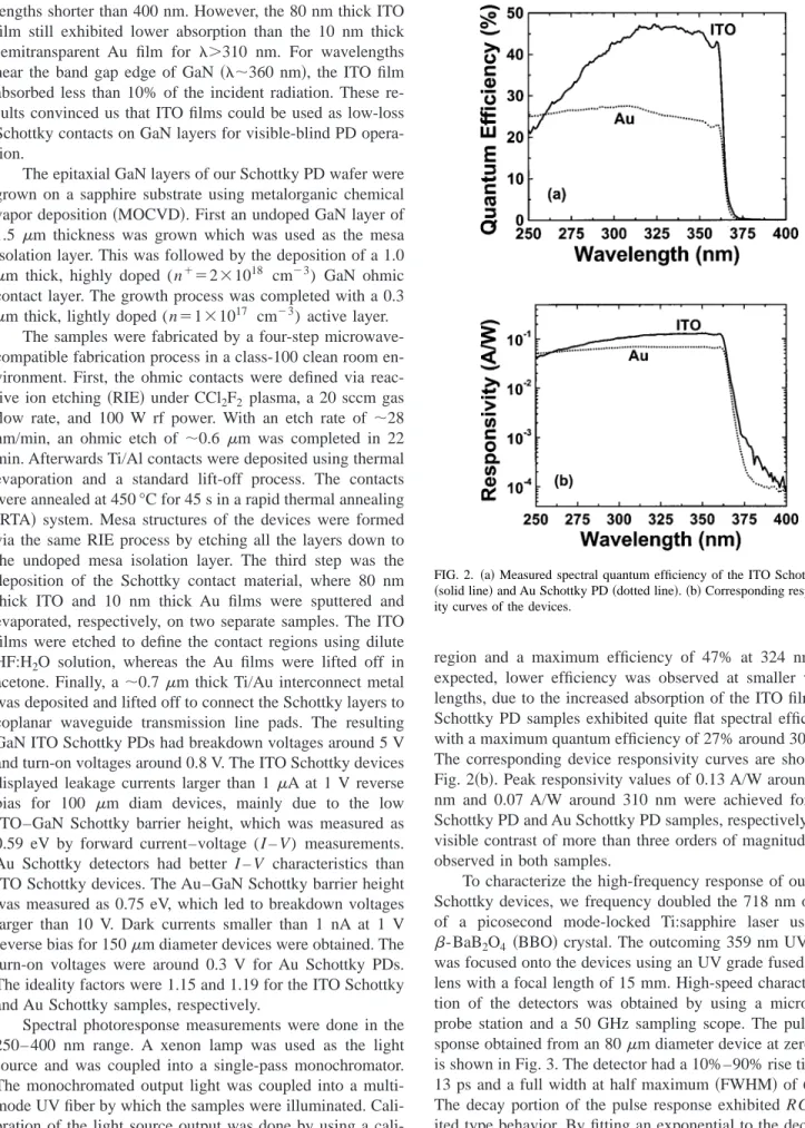
Spectral photoresponse measurements were done in the 250– 400 nm range. A xenon lamp was used as the light source and was coupled into a single-pass monochromator. The monochromated output light was coupled into a multi-mode UV fiber by which the samples were illuminated. Cali-bration of the light source output was done by using a cali-brated Si photodetector. Figure 2共a兲 shows the measured spectral quantum efficiency under zero bias on a linear scale. The ITO Schottky PD samples showed higher efficiency per-formance, with efficiency values ⬎40% in the 290–360 nm
region and a maximum efficiency of 47% at 324 nm. As expected, lower efficiency was observed at smaller wave-lengths, due to the increased absorption of the ITO film. Au Schottky PD samples exhibited quite flat spectral efficiency with a maximum quantum efficiency of 27% around 300 nm. The corresponding device responsivity curves are shown in Fig. 2共b兲. Peak responsivity values of 0.13 A/W around 350 nm and 0.07 A/W around 310 nm were achieved for ITO Schottky PD and Au Schottky PD samples, respectively. UV/ visible contrast of more than three orders of magnitude was observed in both samples.
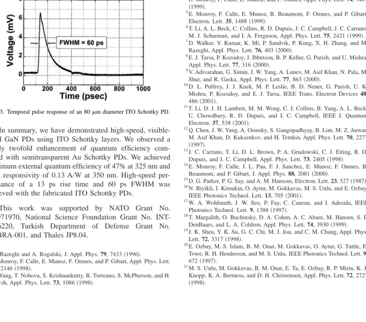
To characterize the high-frequency response of our ITO Schottky devices, we frequency doubled the 718 nm output of a picosecond mode-locked Ti:sapphire laser using a -BaB2O4 共BBO兲 crystal. The outcoming 359 nm UV light
was focused onto the devices using an UV grade fused silica lens with a focal length of 15 mm. High-speed characteriza-tion of the detectors was obtained by using a microwave probe station and a 50 GHz sampling scope. The pulse re-sponse obtained from an 80m diameter device at zero bias is shown in Fig. 3. The detector had a 10%–90% rise time of 13 ps and a full width at half maximum共FWHM兲 of 60 ps. The decay portion of the pulse response exhibited RC lim-ited type behavior. By fitting an exponential to the decaying part, we obtained an RC time constant of 82 ps. This is in good agreement with the calculated RC time constant of 90 ps. The fast Fourier transform of the pulse response yielded a 3 dB bandwidth of 2.6 GHz.
FIG. 2. 共a兲 Measured spectral quantum efficiency of the ITO Schottky PD
共solid line兲 and Au Schottky PD 共dotted line兲. 共b兲 Corresponding
responsiv-ity curves of the devices.
2839
In summary, we have demonstrated high-speed, visible-blind GaN PDs using ITO Schottky layers. We observed a nearly twofold enhancement of quantum efficiency com-pared with semitransparent Au Schottky PDs. We achieved maximum external quantum efficiency of 47% at 325 nm and peak responsivity of 0.13 A/W at 350 nm. High-speed per-formance of a 13 ps rise time and 60 ps FWHM was achieved with the fabricated ITO Schottky PDs.
This work was supported by NATO Grant No. SfP971970, National Science Foundation Grant No. INT-9906220, Turkish Department of Defense Grant No. KOBRA-001, and Thales JP8.04.
1M. Razeghi and A. Rogalski, J. Appl. Phys. 79, 7433共1996兲.
2E. Monroy, F. Calle, E. Munoz, F. Omnes, and P. Gibart, Appl. Phys. Lett. 73, 2146共1998兲.
3
W. Yang, T. Nohova, S. Krishnankutty, R. Torreano, S. McPherson, and H. Marsh, Appl. Phys. Lett. 73, 1086共1998兲.
4E. Monroy, F. Calle, E. Munoz, and F. Omnes, Appl. Phys. Lett. 74, 3401 共1999兲.
5E. Monroy, F. Calle, E. Munoz, B. Beaumont, F. Omnes, and P. Gibart, Electron. Lett. 35, 1488共1999兲.
6T. Li, A. L. Beck, C. Collins, R. D. Dupuis, J. C. Campbell, J. C. Carrano, M. J. Schurman, and I. A. Ferguson, Appl. Phys. Lett. 75, 2421共1999兲. 7D. Walker, V. Kumar, K. Mi, P. Sandvik, P. Kung, X. H. Zhang, and M.
Razeghi, Appl. Phys. Lett. 76, 403共2000兲.
8E. J. Tarsa, P. Kozodoy, J. Ibbetson, B. P. Keller, G. Parish, and U. Mishra, Appl. Phys. Lett. 77, 316共2000兲.
9V. Adivarahan, G. Simin, J. W. Yang, A. Lunev, M. Asif Khan, N. Pala, M. Shur, and R. Gaska, Appl. Phys. Lett. 77, 863共2000兲.
10D. L. Pulfrey, J. J. Kuek, M. P. Leslie, B. D. Nener, G. Parish, U. K. Mishra, P. Kozodoy, and E. J. Tarsa, IEEE Trans. Electron Devices 48,
486共2001兲.
11
T. Li, D. J. H. Lambert, M. M. Wong, C. J. Collins, B. Yang, A. L. Beck, U. Chowdhury, R. D. Dupuis, and J. C. Campbell, IEEE J. Quantum Electron. 37, 538共2001兲.
12Q. Chen, J. W. Yang, A. Osinsky, S. Gangopadhyay, B. Lim, M. Z. Anwar, M. Asif Khan, D. Kuksenkov, and H. Temkin, Appl. Phys. Lett. 70, 2277 共1997兲.
13
J. C. Carrano, T. Li, D. L. Brown, P. A. Grudowski, C. J. Eiting, R. D. Dupuis, and J. C. Campbell, Appl. Phys. Lett. 73, 2405共1998兲. 14
E. Monroy, F. Calle, J. L. Pau, F. J. Sanchez, E. Munoz, F. Omnes, B. Beaumont, and P. Gibart, J. Appl. Phys. 88, 2081共2000兲.
15D. G. Parker, P. G. Say, and A. M. Hansom, Electron. Lett. 23, 527共1987兲. 16N. Biyikli, I. Kimukin, O. Aytur, M. Gokkavas, M. S. Unlu, and E. Ozbay,
IEEE Photonics Technol. Lett. 13, 705共2001兲.
17W. A. Wohlmuth, J. W. Seo, P. Fay, C. Caneau, and I. Adesida, IEEE Photonics Technol. Lett. 9, 1388共1997兲.
18T. Margalith, O. Buchinsky, D. A. Cohen, A. C. Abare, M. Hansen, S. P. DenBaars, and L. A. Coldren, Appl. Phys. Lett. 74, 3930共1999兲. 19J. K. Sheu, Y. K. Su, G. C. Chi, M. J. Jou, and C. M. Chang, Appl. Phys.
Lett. 72, 3317共1998兲.
20E. Ozbay, M. S. Islam, B. M. Onat, M. Gokkavas, O. Aytur, G. Tuttle, E. Towe, R. H. Henderson, and M. S. Unlu, IEEE Photonics Technol. Lett. 9,
672共1997兲.
21M. S. Unlu, M. Gokkavas, B. M. Onat, E. Ta, E. Ozbay, R. P. Mirin, K. J. Knopp, K. A. Bertness, and D. H. Christensen, Appl. Phys. Lett. 72, 2727 共1998兲.
FIG. 3. Temporal pulse response of an 80m diameter ITO Schottky PD.