Post-Treatment of Silicon Nanocrystals Produced by Ultra-Short
Pulsed Laser Ablation in Liquid: Toward Blue Luminescent
Nanocrystal Generation
Sabri Alkis,
†,‡Ali K. Okyay,
†,‡and Bülend Ortaç*
,††UNAM Institute of Materials Science and Nanotechnology and‡Department of Electrical and Electronics Engineering, Bilkent
University, Bilkent 06800 Ankara, Turkey
ABSTRACT: Blue luminescent colloidal silicon nanocrystals (Si-NCs) were produced in a two-stage process. In the first step, synthesis of Si-NCs was achieved by femtosecond pulsed laser ablation of a silicon wafer, which was immersed in deionized water. The size and the structural and the chemical characteristics of colloidal Si-NCs were investigated by TEM and EDAX analyses, and it is found out that the Si-NCs are in spherical shape and the particle diameters are in the range of 5−100 nm. In the second step, ultrasonic waves and filtering chemical-free post-treatment of colloidal Si-NCs solution was performed to reduce the particle size. High-resolution TEM
(HRTEM) studies on post-treated colloidal solution clearly show that small (1−5.5 nm in diameter) Si-NCs were successfully produced. Raman spectroscopy results clearly confirms the generation of Si nanoparticles in the crystalline nature, and the Raman scattering study of post-treated Si-NCs confirms the reduction of the particle size. The UV−vis absorption and photoluminescence (PL) spectroscopy studies elucidate the quantum confinement effect of Si-NCs on the optical properties. The colloidal Si-NCs and post-treated Si-NCs solutions present strong absorption edge shifts toward UV region. Broadband PL emission behavior is observed for the initial colloidal Si-NCs, and the PL spectrum of post-treated Si-NCs presents a blue-shifted broadband PL emission behavior due to the particle size reduction effect.
1. INTRODUCTION
Recent reports show the staggering prospect of nanocrystal quantum dot (NQD)-based nanophosphors for light con-version and color engineering in solid-state lighting and backlighting industries. However, cadmium in efficient NQDs makes them unsuitable for use in environment friendly devices. Providing cadmium-free NQDs in amounts sufficient for the mass production of color-conversion light-emitting diodes (LEDs) is an area in which further research and development effort is needed.1 Silicon, on the other hand, is abundant in nature and environment friendly. In recent years, ultrasmall Silicon nanoparticles were shown to exhibit strong lumines-cence properties. Many research efforts focused on different techniques to produce Silicon nanocrystals (Si-NCs) including chemical vapor deposition (CVD), ion implantation, electro-chemical etching, and laser ablation. Various techniques to obtain luminescent silicon NCs were demonstrated with limited prospects of mass production. CVD methods are widely used to investigate Silicon nanoparticles.2,3 The nanoparticles are obtained in a host matrix such as SiO2 and Si3N4, and the
nanoparticles are isolated from the host matrix through selective chemical removal of the host matrix. High volume of Silicon nanoparticles production is challenging through the CVD methods because it is primarily a surface reaction. Researchers also produced silicon nanoparticles by ion-implantation
of Si species into SiO2layers, followed by surface annealing and
rapid annealing processes.4,5
Nayfeh6,7reported a high throughput and low-cost method for producing silicon nanoparticles of diameters <3 nm. This method is based on electrochemical etching of bulk silicon wafers using a mixture of HF (hydrofluoric acid), hydrogen peroxide (H2O2), and methanol. Upon electrochemical etching, silicon wafer becomes porous, followed by the collection of silicon nanoparticles from the surface by ultrasonic treatment. It has been shown that 1−3 nm size silicon nanoparticles fluoresce in blue, green, and red wavelengths upon excitation with UV illumination.8,9 Optical vibronic and excitonic properties of these ultrasmall nanoparticles have also been obtained both experimentally and theoretically.10
Laser ablation synthesis of nanoparticles is another promising solution.11−14 The interaction of the intense laser light with matter offers an alternative capability to produce NCs.15−33 Laser ablation, especially in liquids, is also a versatile method for colloidal NC synthesis. The generation of Si NCs by laser pyrolysis has been previously demonstrated,16−23 and photo-luminescence (PL) effects of size-separated Si NCs were investigated in the literature.19,21There have been quite a few
Received: November 30, 2011 Revised: December 23, 2011 Published: January 11, 2012
reports on the generation of Si NCs by using nanosecond (ns) and femtosecond pulsed laser ablations in various liquid environments.24−33 Small particles (average size diameter <3 nm) were obtained by femtosecond laser ablation in water.30,31 Particles with diameters of 3−7 nm were also produced by using ns laser ablation in ethanol.32Another strategy that was applied for the generation of small-sized (3−5 nm) Si NCs was ultrasonic chemical post-treatment in HF33after the formation of larger-sized nanoparticles using ns pulsed laser ablation in chloroform. The main drawback of the chemical post-treatment process is the hazardous nature of HF present on post-treated nanocrystals that is critical for applications of nanocrystals in biological systems. In this Article, we report the generation of agent-free blue luminescent colloidal Si NCs by two-stage process: small particles with diameters in the range of 5−100 nm were obtained using femtosecond laser ablation technique, followed by a chemical-free ultrasonic and filtering post-treatment process, which generated ultrasmall (1−5.5 nm) Si NCs. Broadband PL emission of untreated Si NCs and blue-shifted broadband PL emission of post-treated (ultrasound and filtering) Si NCs were observed.
2. EXPERIMENTAL DETAILS
A silicon wafer (99.99%, Cemat Silicon Company) was cleaned by sonification in acetone prior to laser ablation without any additional purification. The generation of colloidal nano-particles from Si wafer was carried out using a commercial Ti:sapphire regenerative femtosecond laser amplifier system operated atλ = 800 nm with pulse duration of 200 fs, average output power of 1.6 W at a pulse repetition rate of 1 kHz corresponding to a pulse energy of 1.6 mJ. The cleaned Si wafer was placed in a glass vessel containing 20 mL of pure deionized water. The laser beam was focused on the target by using a plano-convex lens with a focal length of 50 mm. The height of liquid layer over the Si target is∼5 mm. The laser ablation was carried out for∼5 min, and the laser beam is scanned over the target surface. During the laser ablation, the formation of colloidal nanoparticle solution (CNS) with dispersed nano-particles in liquid media was observed. After the laser irradiation, the color of the CNS became light-orange.
The structural and elemental composition analyses of CNS generated by femtosecond pulsed laser ablation were studied by transmission electron microscope (TEM model FEI - Tecnai G2F30) system equipped with energy-dispersive X-ray (EDAX) system. TEM samples were prepared by drop-casting solutions onto carbon-coated TEM grids. To understand further and better characterize the structure and the composition of post-treated CNS, we performed detailed scanning transmission electron microscope (STEM) study with high-angle annular dark field (HAADF).
Raman spectroscopy studies of the CNS solutions were performed using a Witec Alpha 300S Micro Raman spectrometer with a Nd:YAG laser at an excitation wavelength of 532 nm (laser power: 10 mW) and a Nikon 100× (N.A. = 0.9) air objective. The CNS solutions were drop-cast onto sapphire substrates, and the Raman spectra were recorded at room temperature.
The optical absorption spectra of the CNS containing Si-NCs and post-treated Si-Si-NCs were obtained using a Varian Cary 5000 UV/vis/NIR spectrophotometer in the 190−400 nm wavelength range. PL measurements for colloidal Si-NCs and post-treated Si-NCs solution in deionized water were carried out using a Fluorolog spectrofluorometer (JobinYvon-Horiba) in the 400−650 nm spectral range fitted with a detector (FL-1073) working at 950 V with a Xenon lamp source. The Si-NCs and post-treated Si-NCs CNS samples in deionized water were prepared in quartz cuvettes.
Samples were treated in a Branson 2510 type ultrasonic bath with an operating frequency of 40 kHz. The filtration process was carried out manually with a syringe and using a Minisart high-flow type of commercial filter paper made out of polyether sulfone (PES), and the pore size of this filter paper is 0.1μm.
3. RESULTS AND DISCUSSION
A representative TEM image of the untreated CNS containing Si nanoparticles obtained by laser ablation is shown in Figure 1a. The TEM image clearly shows that Si nanoparticles exhibit spherical-like geometry. The images show that high-energy femtosecond laser ablation of a silicon wafer target in deionized water produced a large particle size distribution. To obtain
Figure 1.(a) TEM image of Si nanoparticles produced by femtosecond laser ablation in deionized water. (b) Size distribution calculated from TEM images of Si nanoparticles. (c) Element mapping EDAX spectrum of Si nanoparticles produced by femtosecond laser ablation.
accurate information about the size distribution of Si nanoparticles, we have counted the sizes of 150 particles seen in the images. The histogram of Si nanoparticle sizes counted from TEM images (Figure 1b) predicts that the particle sizes range from 5.5 to 100 nm. It is found that a large portion of the nanoparticles have diameters of 5.5−40 nm. It should be noted that small particles with sizes less than 5.5 nm are not observed in this study. We also observed particles with sizes larger than 100 nm up to 500 nm, but these particles are not included in the histogram.
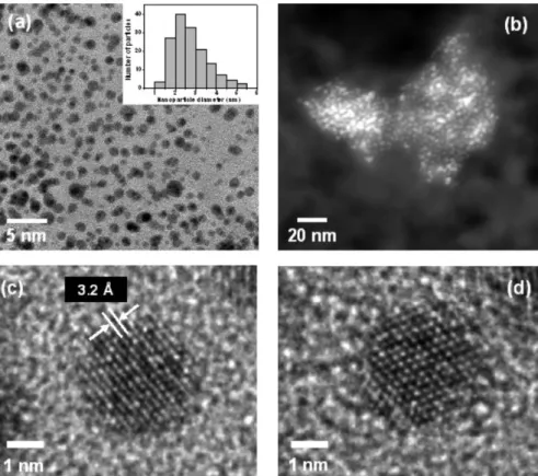
The elemental compositions of the CNS (Figure 1c) were obtained by EDAX analysis. The peaks related to carbon (C), oxygen (O), and copper (Cu) are associated with the TEM grid used. The presence of the Si peak in the EDAX spectrum confirms that Si nanoparticles were successfully generated by laser ablation technique with no significant impurities observed. Following laser ablation, samples were transferred into plastic containers and sonificated for 200 min. The solution was then filtered to remove large-sized particles. TEM image (Figure 2a) and STEM HAADF image (Figure 2b) of the post-treated samples clearly show that spherical ultrasmall nanoparticles were successfully produced by an ultrasonic and filtering post-treatment. TEM studies indicate that no aggregate nano-particles are present, which indicates ultrasmall monodispersed Si nanoparticles generation by post-treatment. The histogram of size distribution of post-treated Si nanoparticles is shown in the inset of Figure 2a, and it predicts that the sizes of small particles range from 1 to 5.5 nm. It should be noted that larger particles with sizes more than 5.5 nm are not observed in this study. The maximum value of this distribution is ∼2 nm. Sonification process reduces particle sizes, and filtration procedure allows large particle elimination.10 This process
finally produces ultrasmall monodispersed Si nanoparticles. Figure 2c presents the HRTEM image of a crystalline 3.5 nm nanoparticle. HRTEM image of a single isolated Si-NC shows the crystalline lattice fringes with lattice spacing of 0.32 nm corresponding to the (111) crystal plane interlayer spacing of Si lattice. (See Figure 2c.) In addition, HRTEM studies also show that cross-lattice planes structure of a single synthesized 3 nm Si-NC is clearly observed. (See Figure 2d.)
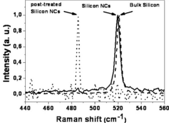
Raman spectroscopy is a very useful technique for the observation of the quantum size effects in nanometer-sized particles and the structural characterization of nanomaterials. In Raman spectroscopy, the vibrational modes in Si nanoparticles can be evaluated due to the bonding effect in Si core by monitoring Si−Si optical phonon vibration.33 The Raman spectrum of Si nanoparticles generated by femtosecond laser ablation in liquid is given in Figure 3 (dashed line), and the spectrum shows a single sharp peak centered at 519.6 cm−1. For comparison, the bulk crystalline Si structure shows a phonon vibration at 520.8 cm−1. (See the dashed line in Figure 3.) The shift to lower frequency of the corresponding Raman modes for the Si nanoparticles can be attributed to the phonon confinement effect due to the nanosized range structure, and the Raman results also confirm the crystalline nature of the Si nanoparticles.33The Raman spectrum of post-treated Si-NCs is shown in Figure 3 (dotted line). A single sharp peak centered at 485.6 cm−1 could be seen in the Figure. The shift to lower frequency of the corresponding Raman modes for the Si-NCs can be attributed to the phonon confinement effect resulting from the reduced nanosized range structure.10
A transmission dip at 265 nm wavelength indicates strong absorption of untreated samples at this wavelength. The filtrated samples exhibit comparatively flat absorption at low
Figure 2. (a) TEM image of Si-NCs after combined ultrasonic and filtering treatment and size distribution calculated from TEM images. (b) Representative STEM HAADF image of Si-NCs. (c) HRTEM image of a single synthesized 3.5 nm Si-NC showing lattice fringe planes. (d) HRTEM image of a single synthesized 3 nm Si-NC showing cross-lattice planes structure.
wavelengths and strong absorption at 237 nm in addition to 265 nm (Figure 4).
To obtain broadband PL emission, the CNS was excited with 370 nm wavelength light. The PL spectrum of Si-NCs dispersed in deionized water is shown in Figure 5 (solid line). PL
spectrum of the Si-NCs solution presents a broadband light emission in the visible range (476 to 616 nm) with an emission maximum at∼490 nm. The quantum confinement effects lead to an efficient light emission in the yellow region of the visible
spectrum, and this PL emission is due to the small particle size of the Si-NCs (size≤10 nm). To monitor the evolution of PL emission behavior, the post-treated Si-NCs were also excited at the same wavelength of 370 nm. This time, a broadband PL emission in the 398−600 nm wavelength range was observed with an emission maximum peak position located at 425 nm (dashed line in Figure 5). The post-treated Si-NCs present very similar broadband PL emission behavior as the initial Si-NCs; however, the PL spectrum of the post-treated Si-NCs shifted to lower frequency (blue-shifted) compared with the optical emission of the initial Si-NCs. The shift to lower wavelength emission for the post-treated Si-NCs can be attributed to the reduction of the particles size, and thus the results clearly demonstrate that we were successful at tailoring the structural and optical properties of Si-NCs through the post-treatment process.
4. CONCLUSIONS
In conclusion, we have demonstrated the generation of blue luminescent Si nanocrystals through a two-stage process, which includes first femtosecond laser ablation of the Si target in liquid, followed by ultrasonic and filtering post-treatment of resulting colloidal Si-NCs solution. As a result of the post-treatment process, ultrasmall (1−5.5 nm in diameter) Si-NCs were successfully produced. The broadband PL emission of initial NCs and the blue-shifted broadband of post-treated Si-NCs were observed due to the particle size effect. This method could be a safe and alternative method to generate ultrasmall Si nanoparticles for biological applications due to its chemical-free nature.
■
AUTHOR INFORMATIONCorresponding Author
*E-mail: [email protected]. Phone: (+90) 312 290 3526. Fax: (+90) 312 266 4365.
■
ACKNOWLEDGMENTSThe State Planning Organization (DPT) of Turkey is acknowledged for the support of UNAM-Institute of Materials Science and Nanotechnology. Dr. Ortaç acknowledges the ‘Industrial Thesis Projects Programme’ of the Ministry of Industry and Trade for funding the San-Tez (636.STZ.2010-1) project. Dr. Okyay acknowledges TUBITAK and EU FP7 for funding 108E163, 109E044, and PIOS 239444 projects. Dr. Alkis acknowledges TUBITAK-BIDEB for research support. We thank Mustafa Güler for TEM imaging and Hüseyin Avni Vural for the histogram of size distribution of Si nanoparticles.
■
REFERENCES(1) Erdem, T.; Demir, H. V. Nat. Photonics 2011, 5, 126.
(2) Nakaso, K.; Han, B.; Ahn, K. H.; Choi, M.; Okuyama, K. J. Aerosol Sci. 2003, 34, 869−881.
(3) Dusane, S.; Bhave, T.; Hullavard, S.; Bhoraskar, S. V.; Lokhare, S. Solid State Commun. 1999, 111, 431−435.
(4) Shimizu-Iwayama, T.; Hama, T.; Hole, D. E.; Boyd, I. W. Nucl. Instrum. Methods Phys. Res., Sect. B 2005, 230, 203−209.
(5) Shimizu-Iwayama, T.; Kurumado, N.; Hole, D. E.; Townsend, P. D. J. Appl. Phys. 1998, 83, 6018−6022.
(6) Akcakir, O.; Therrien, J.; Belomoin, G.; Barry, N.; Muller, J. D.; Gratton, E.; Nayfeh, M. Appl. Phys. Lett. 2000, 76, 1857−1859.
(7) Mitas, L.; Therrien, J.; Twesten, R.; Belomoin, G.; Nayfeh, M. H. Appl. Phys. Lett. 2001, 78, 1918−1920.
Figure 3.Raman spectra of Si-NCs generated by femtosecond laser ablation in liquid (solid line), post-treated Si-NCs (dotted line) and bulk Si wafer used for this experiment (dashed line).
Figure 4. Normalized UV−vis transmission spectra of Si-NCs produced by femtosecond laser ablation in deionized water (solid line) and Si-NCs obtained after post-treatment.
Figure 5.Normalized PL spectra of Si-NCs in deionized water (solid line) and Si-NCs produced after post-treatment.
(8) Rogozhina, E.; Belomoin, G.; Smith, A.; Abuhassan, L.; Barry, N.; Akcakir, O.; Braun, P. V.; Nayfeh, M. H. Appl. Phys. Lett. 2001, 78, 3711−3713.
(9) Belomoin, G.; Therrien, J.; Smith, A.; Rao, S.; Twesten, R.; Chaieb, S.; Wagner, L.; Mitas, L.; Nayfeh, M. H. Appl. Phys. Lett. 2002, 80, 841−843.
(10) Rao, S.; Mantey, K.; Therrien, J.; Smith, A.; Nayfeh, M. Phys. Rev. B 2007, 76, 155316.
(11) Mafune, F.; Kohno, J.; Takeda, Y.; Kondow, T.; Sawabe, H. J. Phys. Chem. B 2000, 104, 8333−8337.
(12) Muramoto, J.; Inmaru, T.; Nakata, Y.; Okada, T.; Maeda, M. J. Phys. Chem. B 2000, 104, 9111−9117.
(13) Mafune, F.; Kohno, J.; Takeda, Y.; Kondow, T.; Sawabe, H. J. Phys. Chem. B 2001, 105, 5114−5120.
(14) Dolgaev, S. I.; Simakin, A. V.; Voronov, V. V.; Shafeev, G. A.; Bozon-Verduraz, F. Appl. Surf. Sci. 2002, 186, 546−551.
(15) Yoshida, T.; Yamada, Y.; Takaaki, O. J. Appl. Phys. 1998, 83, 5427−5432.
(16) Ehbrecht, M.; Kohn, B.; Huisken, F.; Laguna, M. A.; Paillard, V. Phys. Rev. B 1997, 56, 6958−6964.
(17) Khokhlov, E. M.; Kolmykov, D. V.; Kononov, N. N.; Kuzmin, G. P.; Polyakov, S. N.; Prokhorov, A. M.; Sulimov, N. A.; Tikhonevitch, O. V. Laser Phys. 1998, 8, 1070−1073.
(18) Kuzmin, G. P.; Karasev, M. E.; Khokhlov, E. M.; Kononov, N. N.; Korovin, S. B.; Plotnichenko, V. G.; Polyakov, S. N.; Pustovoy, V. I.; Tikhonevitch, O. V. Laser Phys. 2000, 10, 939−945.
(19) Ledoux, G.; Guillois, O.; Porterat, D.; Reynaud, C.; Huisken, F.; Kohn, B.; Paillard, V. Phys. Rev. B 2000, 62, 15942−15951.
(20) Ledoux, G.; Gong, J.; Huisken, F. Appl. Phys. Lett. 2001, 79, 4028−4030.
(21) Ledoux, G.; Gong, J.; Huisken, F.; Guillois, O.; Reynaud, C. Appl. Phys. Lett. 2002, 80, 4834−4836.
(22) Li, X.; He, Y.; Talukdar, S. S.; Swihart, M. T. Langmuir 2003, 19, 8490−8496.
(23) Lacour, F.; Guillois, O.; Portier, X.; Perez, H.; Herlin, N.; Reynaud, C. Physica E 2007, 38, 11−15.
(24) Švrček, V.; Sasaki, T.; Shimizu, Y.; Koshizaki, N. Appl. Phys. Lett. 2006, 89, 213113.
(25) Yang, S.; Cai, W.; Zeng, H.; Li, Z. J. Appl. Phys. 2008, 104, 023516.
(26) Semaltianos, N. G.; Perrie, W.; Vishnyakov, V.; Murray, R.; Williams, C. J.; Edwardson, S. P.; Dearden, G.; French, P.; Sharp, M.; Logothetidis, S.; Watkins, K. G. Mater. Lett. 2008, 62, 2165−2170.
(27) Kuzmin, G.; Shafeev, G. A.; Bukin, V. V.; Garnov, S. V.; Farcau, C.; Carles, R.; Warot-Fonrose, B.; Guieu, V.; Viau, G. J. Phys. Chem. C 2010, 114, 15266−15273.
(28) Amoruso, S.; Bruzzese, R.; Spinelli, N.; Velotta, R.; Vitiello, M.; Wang, X.; Ausanio, G.; Iannotti, V.; Lanotte, L. Appl. Phys. Lett. 2004, 84, 4502−4504.
(29) Semaltianos, N. G.; Logothetidis, S.; Perrie, W.; Romani, S.; Potter, R. J.; Edwardson, S. P.; French, P.; Sharp, M.; Dearden, G.; Watkins, K. G. J. Nanopart. Res. 2010, 12, 573−580.
(30) Rioux, D.; Laferriere, M.; Douplik, A.; Shah, D.; Lilge, L.; Kabashin, A. V.; Meunier, M. M. J. Biomed. Opt. 2009, 14, 021010.
(31) Intartaglia, R.; Bagga, K.; Brandi, F.; Das, G.; Genovese, A.; Di Fabrizio, E.; Diaspro, A. J. Phys. Chem. C 2011, 115, 5102−5107.
(32) Yang, S.; Cai, W.; Zhang, H.; Xu, X.; Zeng, H. J. Phys. Chem. C 2009, 113, 19091−19095.
(33) Abderrafi, K.; Calzada, R. G.; Gongalsky, M. B.; Suarez, I.; Abarques, R.; Chirvony, V. S.; Yu, V.; Timoshenko, R. I.; Martínez-Pastor, J. P. J. Phys. Chem. C 2011, 115, 5147−5151.