ProQedings of the 1991 IEEE
Intemationai Conference on Robotics and Automation Sacramento, California
-
April 1991An
Automatled System for Design-Rule-Based Visual Inspection of
Printed Circuit Boasds
Seyfullah Halit OGUZ and Levent ONUR-4L
Electrical and Electronics Engineering Department
Bilkeiit University
Bilkent 06533, Ankara, Turkey
Abstract
In this paper, the design and the implementation of an automated, design-rule-based, visual priiited circuit board (PCB) inspection system are presented. The developed system employs mathematical morphology based image processing a1gorith.m.s. This system d e - tects PCB defects related to the conducting structures on PCBs b y checking a set of geometric design rules. For th,is purpose, a new image segmentation algorithm and a new defect detection algorithm are designed. The defect detection algorithm is capable of verifying the minimum conductor spacing, minimum conductor trace width, and the minimum land width requirements on digital binary PCB images. Also, an already exist- ing defect detection algorithm is modijed for its im- plementation in our system. A prototype system is implemented in our image processing laboratory.
1
Introduction
In this work, the design and the implementation of a system which is capable of automatically performing the visual pattern inspection of printed circuit boards are accomplished. The automation of the visual in- spection process of PCBs is indispensable in order to maintain and improve the productivity of PCB man- ufacturing. Due to its various advantages and flex- ibility in use, a design rule based system is devel- oped. This system makes use of defect detection algo- rithms which are derived using image transformations based on mathematical morphology. In this study, only the detection of the defects related to the con- ducting structures on the PCBs is considered. For the implementation, we began with the initial work for determining and classifying the defects to be de- tected. The following classification is made for the defects planned to be detected:
1. Defects related to the violation of the minimum land width (MLW) requirement.
2. Defects related to the violation of the minimum
conductor spacing (MCS) requirement.
3. Defects related to the violation of t,he minimum
conductor trace width (MCTW) requirement. In the next step, the desigil rules which govern the ap- pearance of different conducting structures on PCBs are determined. The design rules mentioned above are described in the form of (geometric) criteria that set such physical constraints as the width and clearance (separation) of conductor traces. In this phase of the work, we assumed the following rules for printed cir- cuit pattern geometry on PCBs:
e Patterns are constructed mainly by conductor traces of arbitrary inclinations and widths.
A minimum and a maximum limit exist for conduc-
tor trace widths and these two limits are common to all conductor braces on the PCB.
e A minimum limit exists for conductor trace separa- tions and this limit is common to all substrate gaps in between conductor traces.
e Undrilled pads of arbitrary shapes are allowed but if holes (either t,hrough holes or vias) exist on the PCB, then the lands surrounding these holes should be annu- lar sha.ped, and, a minimum limit exists for the widths of these annular lands mThere this limit is common to all lands on the PCB.
Then, we designed appropriate mathematical mor- phology based algorithms those are capable of verify- ing the design rules and detecting, locating, and clas- sifying any violations. For this purpose, two new al- gorithms (an image segmentation algorithm specially designed for PCB images, and a defect det,ection algo- rithm capable of detecting the previously mentioned 3
major classes of PCB defects after some proper param- eter changes) are developed, and another defect detec- t.ion algorithm due to [7] is modified for implementa- tion on our image processor. Later, we determined the most time-efficient realizations of the proposed mor- phological image processing algorithms where the tools (hardware) to be used for implementation and thus
their capabilities are fixed. After the deterinination of the most efficient realization methods, two system pro- grams are generated for defect detection on
PCBs.
As for the interpretation step, the verifications of both the defect detection algorithms and the developed system software are made by many test runs of the software on some sample PCBs and a master artwork containing many typical defects. In this way, a prototype real- ization of the rule based visual inspection system is completed in our image processing laboratory.2
Mathematical hlorphology
There is an extensive and yet increasing literature on mathematical morphology and for this reason, instead of supplying precise definitions of mathematical mor- phology here, we will only describe qualitatively the fundamental operations, and direct the reader to three of the related excellent references, [l],[a],
[3]. Hit or Miss transformation is a template matching pro- cess where the Hits are marked by foreground pixels (with value 1) and the Misses are marked by back- ground pixels (with value0).
Erosion operation as the name suggests, tappers the foreground structures and may alter the connectivity properties of the image. Dilation operation enlarges the foreground structures and may also alter the connectivity properties of the A skeletal element is a foreground pixel that isnecessary to maintain the 8-connectivity of its 8- neighborhood; i.e. changing the pixel to a back- ground pixel breaks the 8-connectivity between at least two other foreground pixels in the 8-neighborhood.
An n-join is a foreground pixel with n foreground 8-
neighbors; hence, a join can be of order 0 to 8. A
T-join
is a 3-join whose 8-neighborhood contains only skeletal elements. ([3],[4])
Symmetrical thinning algorithm tappers the fore- ground structures without altering the connectiv- ity properties of the image. Pruning algorithm trims “hair” like protrusions which may result as an artifact of the symmetrical thinning operation. In this work, a symmetrical thinning and a pruning algorithm based on the cascade implementation of [5] are used. image.
(PI, PI)
3
Defect Detection Algorithms
3.1 Isotropic Structuring ElementsIn order to check a common minimum width require- ment on a binary image in the Euclidean %space,
E 2 , containing some foreground stripes of arbitrary
widths and inclinations, one can consider the enclo- sure of a single circular structuring element (SE) into the stripes. This isotropic SE having the common
minimum width as its diameter enables the use of a single template on all foreground stripes with arbi- trary inclinations.
A similar problem in the discritized Euclidean 2-space,
Z 2 , can be handled by considering discrete approxima-
tions to circular structures. These approximate SEs must have the following two necessary features. They must be as similar as possible t o the original circular structure and decomposable into a dilation of smaller sized SEs. This last condition is related to implenien- tation considerations. In general octagonal SEs have these two features.
In case of rectangular sampling with unequal horizon- tal and vertical sampling periods, the isotropic SEs turn out to be elliptic structures with a fixed axis length ratio. The similarity and decomposability re- quirements are also to be satisfied. In this work, due to our available hardware, we extensively used discrete approximations to elliptic structures.
3.2 Algorithm for Removing Lands
Given a
P C B
image with drilled through holes and vias, this new image segmentation algorithm removes the conductor lands surrounding these holes from the image and thus generates t ~ 7 o binary images, one con- taining only the conductor traces and the other only the lands surrounding the holes. This enables the ap- plication of only the related design rule checking al- gorithms t o these structures and hence avoids false alarms. This algorithm works as follows:1. A 3 level digital image is captured from the
P C B
(Figure 1.a). In this image, pixels with the medium gray level have value 0 and indicate the substrate, black pixels having value 1 indicate the coiiducting structures, and the white pixels having value 2 indi-
cate the places where there are holes.
2 . The following look-up table (LUT) transformation
is applied to the image of Figure 1.a in order t o ex- tract the locations of the holes. 0 -+ 0, 1 -+ 0, 2
-
1.Figure 1.b shows the resultant binary image.
3. The image of Figure 1.b is dilated with an isotropic SE (an elliptic one). Hence, as seen in Figure l.c, the hole locations are enlarged so as to cover their sur- rounding lands.
4. The following LUT transformation is applied to the image of Figure 1.a t o extract only the conducting structures. 0 -+ 0, 1 -+ 1, 2 -+ 0. Figure 1.d shows the resultant binary image.
5. The images of Figure 1.c and Figure 1.d are logi- cally ANDed. The resultant binary image, Figure l.e, contains only the lands.
6. The images of Figure 1.d and Figure 1.e are logi- cally EXORed. The resultant binary image given in
Figure 1.f contains only the conductor traces.
3.3 Algorithm Verifying MCS Requirement
This new algorithm checks the MCS requirement on binary PCB test images and directly detects the viola- tions and also their places without the need for a time consuming comparison step which is typically needed in most of the similar applications [4], [5], [6]. The algorithm works as follows:
1. The original PCB test image (Figure 2.a) to be in- spected against defects is dilated once by an isotropic
SE (an elliptic one). This SE is specifically designed to induce new symptomatic foreground connections be- tween neighboring conducting structures only at the defective places. Figure 2.b shows the resultant im- age.
2. The image of Figure 2.b is symmetrically thinned so that the symptomatic festures are preserved and the pixels in the resultant image, Figure 2.c, reduce to either symptomatic pixels or pixels present in the original image.
3. The image of Figure 2.c is pruned so that possible false alarms due to “hair” like protrusions are avoided. Figure 2.d shows the resultant image.
4. The images of Figure 2.a and Figure 2.d are logi- cally ORed. As seen in the image of Figure 2.e, this results in the inclusion of the symptomatic pixels into the original image.
5. The images of Figure 2.a and Figure 2.e are logically EXORed. This step extracts only the pixels which are not common in the above mentioned images. As Fig- ure 2.f shows, these are the Symptomatic pixels show- ing the defective locations.
3.4 Algorithm Verifying MCTW Requirement
For detecting MCTW violations, we note that the MCTW requirement in the original image can be inter- preted as the minimum spacing requirement between the substrate traces in the (bitwise) complemented im- age. Hence, in order to detect this class of defects we apply the algorithm given in Section 3.3 to the back- ground of the test images with appropriate parameter changes in the algorithm. These parameter changes cover the SE, and the number of symmetrical thinning and pruning operations applied to the background pix- els.
3.5 Algorithm Verifying MLW Requirement
Since the lands are in the form of ring shaped conduc- tor traces, the extension of the algorithm of Section 3.4 to the case of lands is rather straightforward. Hence, we apply the algorithm of Section 3.4 to a subimage containing the lands only, after appropriate parameter
changes in the algorithm. As before, these parameter changes cover the SE, and the number of symmetrical thinning and pruning operations applied to the back- ground pixels.
3.6 An Algorithni to Supersede the Algorithms
of Sections 3.3 and 3.4
Although the two defect detection algorithms of Sec- tions 3.3 and 3.4 work very well, for an industrial ap- plication of the system a faster algorithm was needed to replace them. Such an algorithm proposed in [’i] was based on a special purpose hardware architecture and had some uncommon features which made it im- possible to be implemented in a useful way on a gen- eral class of image processors. So we had to adopt the implementation technique by keeping the idea of the algorithm essentially the same. The algorithm as im- plemented by our modified technique and used in our system works as follows:
1. The original PCB test image, Figure 3.a, to be in- spected against defects is dilated once by a properly chosen isotropic SE. This step has exactly the same significance as the first step of the algorithm given in Section 3.3. Figure 3.b shows the resultant image. 2. Images of Figure 3.a and Figure 3.b are logically EXORed. This operation as can be seen in the resul- tant image of Figure 3.c, induces some “T” shaped foreground structures only in the defective places. These structures which are certain to reduce t o “T joins” after symmetrically thinning the image of Fig- ure 3.c down to its skeleton, constitute the symp- tomatic features we want to induce. The places where there are no defects, will reduce to connected chains of “2 joins” after appropriate symmetrical thinning. 3. In order to induce similar symptomatic features at the defective places where the MCTW requirement is violated, we proceed as follows. The original PCB test image given in Figure 3.a is eroded once by a prop- erly chosen isotropic SE. This step induces new symp- tomatic background connections at the places where
the MCTW requirement is violated. Figure 3.d shows
the resulting image.
4. Images of Figure 3.a and Figure 3.d are logically
EXORed. This operation as can be seen in the re- sultant image of Figure 3.e, induces some “T” shaped foreground structures only in the defective places. As can be easily judged, this step has exactly the same significance as the second step of this algorithm.
5. At this point, in order to speed up the algorithm we note that exactly similar kinds of further process- ing is required on the images of Figure 3.c and Figure 3.e. We should symmetrically thin both of the im- ages and detect the places of “T joins”. In fact, even
exact skeletonization (i.e. application of the symmet- rical thinning operation until idempotance), which is very time consuming, is not required. Instead, we can skeletonize only the defect-free places (i.e, generate connected curves of “ 2 joins” in defect-free places), and generalize the class of symptomatic features from “T joins” to “all joins except 2 joins”. This will speed up the algorithm further and also enable us to detect some defects which otherwise we wouldn’t be able to detect. To perform the common further processing on both of the images simultaneously, we can combine these two nonoverlapping images. But, in order not t o miss some Symptomatic features, before combining the two images we make them spatially disjoint (separated) by an appropriate sequence of symmetrical thinning and pruning operations. The resultant images obtained af- ter the application of this processing to the images of Figure 3.c and Figure 3.e are shown in Figure 3.f and Figure 3.g, respectively.
6. The images of Figure 3.f and Figure 3.g are log- ically ORed. As Figure 3.h shows, by this operation we achieve our goal of combining these two images into one which contains all of the symptomatic features of both images.
7. The image of Figure 3.11 is synimetrically thinned and pruned for a sufficient number of times so that the defect-free places are reduced to connected curves of
“2-joins”. Figure 3.i shows the resultant image.
8. In the image of Figure 3.i, the positions of the joins of order different than 2 are extracted. The result of this operation is shown in Figure 3.j. The foreground pixels in this image show the defective places where the design rules related to the &ICs or to the MCTW requirements are violated.
9. As a final step, our defect detection software encir- cles the defective locations by red colored rectangular frames on the gray level test image captured from the PCB. This operation is shown in Figure 3.k.
3.7 Iniplementation of Morphological Opera-
tions
A straightforward implement,ation of morphological operators employing SEs of size at most 3x3, by us- ing 3x3 2-D convolution followed by a table lookup operation, is mentioned in [SI. The fundamental algo- rithm proposed in this reference, requires the use of a 512 entry lookup table. In the same reference, an adopted version of this algorithm so as to take into account the implementations based on lookup tables restricted to 256 entries is also given. However, our im- age processor containing 256 entry lookup tables does not enable ai1 efficient implementation based on this modified technique due t o its hardware architecture.
For this reason, we had to find another implementa- tion technique. The technique we propose is similar to the technique of [8], however we relax the condition of exactly determining the pixel distribution under the convolution kernel. Instead, we choose the convolution kernel elements such that the result of the convolution on a 3x3 neighborhood specifies the image pixel distri- bution in that 3x3 neighborhood (of the image) just with sufficient information so that the correct decision can be made about the morphological operation’s re- sult in that neighborhood. For example, in the case of implementing the Hit or Miss transformations, the detection of the presence of a foreground pixel in a lo- cation where a background pixel should exist, or vice versa, specifies the resultant pixel uniquely. For this purpose, in choosing the convolution kernel elements, we make use of the significance of each pixel in the SE
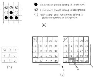
in terms of its effect on the result. An example will clarify the principles of the technique we propose. In Figure 4, the implementation of a single element fore- ground thinning operation is considered. This opera- tion requires the implementation of Hit or Miss trans- formation followed by an EXOR operation. Both of these operations will be realized in a single step. In part (a) of this figure the thinning SE to be imple- mented is given. Part (b) of the same figure shows the 2-D 3x3 convolution kernel elements chosen. As can be seen, equal convolution kernel values are as- signed to pixels in the SE which should belong to the background ( l o ) , or to the foreground (2). “Don’t Care” pixel locations are weighted by zero. The only departure from this convention is in the center pixel w-hich is weighted by 5 although it should belong to the foreground. In fact such a choice is indispensable, since in case of a Miss we should carry the pixel value in the original image to the thinned image without any change and for this reason we should be able t o uniquely identify the value of the center pixel in the original image. In Figure 4.c, based on this argument, the entries of the LUT to be used lo transform the con- volution results to binary pixel values are given. This table covers all possible convolution results performed on a binary image and all other entries of the LUT not listed in this table are “Don’t Care” conditions. Note that the convolution result corresponding to a Hit is 11, and in this case the center pixel in the original im- age which is a foreground pixel is subtracted from the original image and replaced by a background pixel in the thinned image. In case of all other entries corre- sponding to Miss conditions, the original value of the center pixel is not changed in the thinned image.
References
J . Serra, Mathematacal Morphology and Image Analyszs, Academic Press, New York, 1982.
R.M. Haralick, S.R. Sternberg, X. Zhuang, “Image Analysis Using Mathematical Morphology,” IEEE Trans. Pattern Anal. Machzne Intell., vol. PAMI-9,
T.Y. Kong, A. Rosenfeld, “Digital Topology: In- troduction and Survey,” Comput. Vtszon Graphzcs Image Process. 48, 1989, pp. 357-393.
J . R . Mandeville, “Novel Method for Analysis of Printed Circuit Images,” IBM J. Res. Dezlelop.,
vol. 29, no. 1, January 1985, pp. 73-86.
A.M. Darwish, A.K. Jain, “A Rule Based Ap-
proach for Visual Pattern Ins~ection.” IEEE
July 1987, pp. 532-550.
Trans. Pattern Anal. Machzne Intell., vol. PAMI-
10, January 1988, pp. 56-68.
A.E. Kayaalp, R. Jain, “Inspection of IC’s for Ran- dom Pattern Defects Using SEhI Images,” College of Engineering, The University of Michigan, Ann Arbor, Michigan; Program in Automated Semicon- ductor Manufacturing, October 1985.
Q.-Z. Ye, P.E. Danielsson, “Inspection of Printed Circuit Boards by Connectivity Preserving Shrink- ing,” IEEE Trans. Pattern Anal. Machzne Intell.,
vol. PAW-10, September 1988, pp. 737-742. F.A. Gerritsen, P.W. Verbeek, “Implementation of Cellular-logic Operators Using 3*3 Convolution
and Table Lookup Hardware,” Comput Vision Graphics Image Process. 27, 1984, pp 115-123.
Figure 3 . Example for the algorithm of Section 3.6.
Pixel which sliould belong t o roregroun(i.
P i x e l Vtl,ich sllould belong to background. I,-) " D o n ' t care" pixel which may belong t o
,.-7 e i t h e r ioreground or background
mi
Fa-
6 16 26 3 i( i( 0 0 (h) I(4
Figure 4. Example for the algorithm of Section 3.7, (a) the structuring element nts, (c) lookup table contents. (b) convolution kernel coefficie