Design of Multi-Octave Band GaN-HEMT Power
Amplifier
Gulesin Eren#, Ozlern A. Sen#, Basar Bolukbas#, Gokhan Kurt#, Orkun Arican#, Orner Cengiz#, Sila T.K. Unal#, Yildirirn Durrnus# and Ekmel Ozbay#
#Department of Electrical and Electronics Engineering, Nanotechnology Research Center, Bilkent University, 06800 Ankara, Turkey
Abstract-This paper describes design, fabrication and measurement of 6 GHz - 18 GHz monolithic microwave integrated circuit (MMIC) amplifier. The amplifier is realized as coplanar waveguide (CPW) circuit using 0.3 /.lm-gate Gallium Nitride (GaN) HEMT technology. The amplifier has a small signal gain of 7 ± 0.75 dB. The output power at 3dB compression is better than 24 dBm with 16%-19% drain efficiency for the whole 6 GHz-18 GHz frequency band under continuous wave (CW)power.
Index Terms-GaN HEMT, amplifier, multi-octave bandwidth, wide-band matching networks, gain equalization networks.
I. INTRODUCTION
Wide-band amplifiers are important for electronic warfare, instrumentation, radar applications. Due to physical properties, Gallium-Nitride (GaN) has become the promising material of choice for wideband power amplifiers.
Fully monolithic microwave integrated circuits realized with gallium nitride (GaN) high electron mobility transistors are of interest to design and implement microwave power amplifiers due to its superior properties like high breakdown voltage, high current density, high thermal conductivity and high saturation current [1]. Large band gap energy and high saturation velocity of AIGaN/GaN high electron mobility transistors (HEMTs) are attractive features for high power applications compared with the conventional material for high power applications- gallium arsenide (GaAs). Wide bandgap nature of GaN makes the material more advantageous than GaAs for the operations that requires high voltage, power and temperature. The high power capability of GaN enables us to make devices with smaller size than of GaAs based devices for the same output power. Thus, device impedances in GaN technology are higher than the GaAs technology which makes broadband matching easier [2].
In this paper, we proposed a multi-octave MMIC amplifier realized with dimensions of 3.5 x 1.5 mm2 by using reactive matching topology. The amplifier is a coplanar single stage MMIC amplifier operating between 6 GHz and 18 GHz suitable for electronic warfare applications. In the first section fabrication details and performance of GaN transistor is summarized. Then, the design procedure of the amplifier is given. Finally measured performances of the fabricated MMICs comparing with our electromagnetic simulations are presented. The design phase was required special attention on
978-1-4673-5696-1112/$26.00 ©2012LEEE
gain flatness of small-signal response and broadband reactive matching networks over the 6-18 GHz bandwidth. The MMIC amplifier realization in a multi-octave bandwidth was performed by using a high electron mobility transistor of 4x75 /lm in coplanar technology which was processed at our own clean-room facilities.
II. TECHNOLOGY AND TRANSISTOR PERFORMANCE The MMIC process has been developed using our 4-inch GaN HEMT on semi-insulating SiC substrate. SiC is used as a substrate material for this application due to its high thermal
GaN 2DEG
s.i SiC Substrate
Fig. I. Cross-sectional view of MMIC
conductivity property. The epitaxial GaN/AIGaN layers are grown on SiC substrate by utilizing MOCVD. Fabrication process consists of formation of Ohmic contact for drain and source connections, Schottky contact for gate metallization, SiN passivation and several inter-process steps. Cross sectional view of a MMIC is given in Fig. 1.
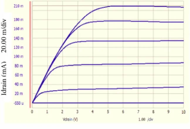
The 4x75 /lm active device cell was characterized by DC IV, S-parameters, and load-pull characterizations. DC characterization result of 4x75 /lm device is given in Fig. 2.
�
a O 0 ci N�
E
.§
'-< :::: 210m 180m 160m 140m 120m 100m 80m 60m 40m 20m -5-50u VdrainM Vdrain (V) 1.00/div�
r
7 8 1.00 1<fN t-� � 101.15A/mm peak drain current density, 270 mS/mm maximum transconductance, 40 GHz of
t:nax
values are achieved from the fabricated 4x75 11m GaN HEMT.III. WIDEBAND DESIGN CONSIDERATIONS
Design process of the wide-band MMIC amplifier is described in this section. Unconditional device stabilization and broadband matching topology design require special attention. Reactive matching topology was found to be the most appropriated topology to fulfill design specifications.
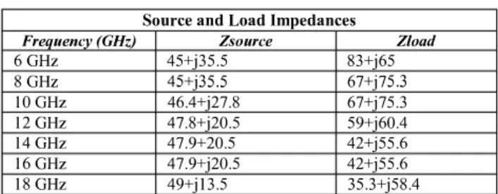
Unconditional stability can be obtained by different networks. In this work adding a parallel combination of R and C in series at the input of the amplifier is chosen as stabilization network since this topology serves for both stabilization of the device and flattening the gain response by decreasing the HEMTs intrinsic gain at lower frequencies. After the stabilization realization, load-pull and source pull simulations are implemented. Table I shows the values of source and load impedances at VDs=15V, and
IDrain=72
mAo Due to the choice of GaN technology, source and load impedances are not so far from the 50 n system impedance and realization broadband matching would not require high impedance transformation ratio so the complexity of the wideband matching topology decreases [4].TABLE I
Source aud Load Impedances
Frequency (GHz) Zsource Zload
6 GHz 45+j35.5 83+j65 8 GHz 45+j35.5 67+j75.3 10 GHz 46.4+j27.8 67+j75.3 12 GHz 47.8+j20.5 59+j60.4 14 GHz 47.9+20.5 42+j55.6 16 GHz 47.9+j20.5 42+j55.6 18 GHz 49+j 13.5 35.3+j58.4
The drain and gate bias circUltnes were designed using rectangular coplanar inductors in order to satisfy wideband requirement.
The empirical adjustments of bias lines are verified using electromagnetic simulations with the realized bypass capacitances.
Gain flatness is the main goal of our amplifier so in addition to gain equalization network, input and output matching topology is optimized for this purpose. The aim for this amplifier is to achieve small signal gain of 7±1 dB for 6 GHz-18 GHz frequency band
While designing the amplifier that covers broadband frequency range, multi-section matching elements have been achieved with the coplanar components.
The output matching network was designed by taking consideration into load-pull simulation data at discrete frequencies over the whole band using five section band-pass Chebyshev-type matching circuitry. Also, the output matching network utilizes from multi-section components like rectangular inductors and open stub CPW lines. Open circuit CPW lines are used instead of MIM capacitors due to better
matching performance at frequency of 18 GHz. Although it is possible to use short circuited stubs instead of coplanar rectangular inductors in output matching circuitry, it is not preferred since it affects the broadband response negatively.
The input matching circuit was realized by supplying a simpler and minimized matching topology using reactive matching circuit with gain equalization network. Similar to the output matching network, shunt capacitances are realized as open stub CPW line instead of MIM capacitors. The MIM capacitances are used as DC block capacitances.
The RF performance of the MMIC amplifier was simulated accurately using Momentum simulation tool of Agilent's Advanced Design System (ADS).
Fig. 3 is a photograph of our fabricated GaN MMIC amplifier. The chip size of the device is 3.5mm x 1.5 mm.
Fig. 3. Photograph of the GaN MMIC
IV. AMPLIFIER PERFORMANCE
The small-signal response of the amplifier by comparing with the simulated small-signal gain (S21) is shown in Fig. 4. In both simulation and measurement drain voltage of the amplifier is taken as 15 V. The design goal for the small signal gain was 7±1 dB. The measured small signal gain varies between 6.3 dB and 7.5 dB within the entire frequency band. We have demonstrated that the resulting device gives compatible outcomes with the simulated small signal gam, input and output return losses.
20�---.---.---.---r 10�-�---+---+---�---�
�
� O �---1---+---�\--�---�rJl
c(j
$'
-1 0 �-j,---,¥'---'.---+---."'C""...!.--t\ "''---� � ,;:; -20Solid: Meas rement
--S2rgFeefl-t---1I---M----"'r---� S'I red
� :
5 S22 blue ... v 10 15 Frequency (GHz) 20 25 10 8 6 4 2 0Fig. 4. S- parameters (S21 (green), Sll( red) and Sn (blue» from the simulation (dotted line) and form measurement (solid line) of the MMIC
�
rJl
ADS harmonic balance simulation results of the amplifier under different input power conditions for 6 GHz, 8 GHz, 10 GHz, 12 GHz, 14 GHz, 16 GHz and 18 GHz are given Fig. 5. As can be seen, saturated CW power is above 22 dBm for all frequencies.
S
� � .. '" � 0 Q.; .... = .e-= 0 26 24 22 20 18 16 14 -12 4I
�
�
=::::::::::
�
r--....V
�
�
�
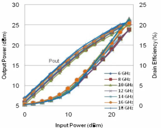
-; 6 8 10 12 14 16 18 20 22 Input Power (dBm)Fig. 5. Simulated CW power vs input power at different frequencies Fig.6 shows output power and efficiency for the swept CW input power of the MMIC for different frequencies. Output power of 24 dBm at 3 dB compression point was achieved over intended frequency. The measurement results are even 1-2dB better than the simulated output power results.Fig.7 shows measurement results of the large signal performance of
30 25 25 20
E
�
Cl � 15 >-20 u :;; c: Q) :;; ." 0 "" 0.. W :; 15 10 c: B-" ·iii Ci 0 __ 8GHz 10 10 . .GW 5 -..-12GHz __ 14GHz __ 16GHz 0 5 ---+-18 GHz 0 10 20 Input Power(dBm)Fig. 6 Measured CW output power and drain efficiency vs input power at different fTequencies
the MMIC over the band of interest using 50% pulsed signal source. The pulsed output power larger than 27 dBm can be obtained over the 6 to 18 GHz band at 3 dB compression point with 47% peak drain efficiency when biased at 15 V. Since the temperature rise is not as much as in CW measurement, higher output power levels are achieved and pulsed mode of operation is required for most of the applications. This measurement also shows that if temperature rise is controlled in CW mode, higher output powers can be obtained.
30 50 45 25 40
E
35�
OJ � 20 30 () Q:; c <V 3: 25 ·u 0 "" 0.. W "5 15 20 c .e-'" .;;; 150
0 10 10 Z 5 5 Z 0 0 5 10 15 20 25 Input Power (dBm)Fig. 7. Measured pulsed output power and drain efficiency vs input power at different fTequencies
v. CONCLUSION
Using a 0.3 11m GaN HEMT technology, a multi-octave band GaN-HEMT MMIC amplifier has been realized with reactively matching topologies. For the 6-18 GHz band, measurement results demonstrate a small signal gain of 7 ± 0.75 dB and minimum 500 mW output power for 3 dB compression point in pulsed mode with related power added efficiency above 35%.
The measured performances of the realized MMICs are in good agreement with electromagnetic simulation predictions.
ACKNOWLEDGEMENT
The authors would like to acknowledge Ayca Emen, Burak Turhan, Dogan Yllmaz, and Huseyin Cakmak for valuable fabrication support.
REFERENCES
[1]
E. Reese, D. Allen, C. Lee, and T. Nguyen, "Wideband power amplifier MMICs utilizing GaN on SiC," 20 10 IEEE MTT-S International Microwave Symposium Digest, pp. 1230 - 1233, June 2002 .[2] U. K. Mishra, P. Parikh, and Y. Wu, "AIGaNiGaN HEMTs- An Overview of Device Operation and Applications," Proceedings of IEEE, vol. 90, no. 6, pp. 1022-1031, June 2002 .
[3] J.W. Milligan, S. Sheppard, W. Pribble, Y.-F. Wu, St.G. Muller, and J.W. Palmour, "SiC and GaN Wide Bandgap Device Technology Overview," IEEE Radar Conference , pp.960-964, April 2007. [4] F. Yamada, S. Mizuno, H. Yamamoto, S. Sano, "A 6 GHz-15GHz 2
Watts GaN MMIC," Proceedings of APMC 2011, pp. 1554-1557, December 20 I 1.
[5] F. van Ray, R.Quay, R. Kiefer, F. Benkhelifa, B. Raynor, W. Pletschen, M. Kuri, H. Massier, S. MUller, M. Dammann, M. Mikulla, M. Schlechtweg "A Coplanar X-band AIGaN/GaN Power Amplifier MMIC on s.i. SiC Substrate," IEEE Microwave and Wireless Component Letters, vol. IS, pp. 460-462.