Metal-semiconductor-metal ultraviolet
photodetectors based on gallium
nitride grown by atomic layer
deposition at low temperatures
Burak Tekcan
Cagla Ozgit-Akgun
Sami Bolat
Necmi Biyikli
Ali Kemal Okyay
Metal-semiconductor-metal ultraviolet photodetectors
based on gallium nitride grown by atomic layer
deposition at low temperatures
Burak Tekcan,a,b,*Cagla Ozgit-Akgun,b,cSami Bolat,a,bNecmi Biyikli,b,cand Ali Kemal Okyaya,b,c
aBilkent University, Department of Electrical and Electronics Engineering, Ankara 06800, Turkey bBilkent University, National Nanotechnology Research Center, Ankara 06800, Turkey
cBilkent University, Institute of Material Science and Nanotechnology, Ankara 06800, Turkey
Abstract. Proof-of-concept, first metal-semiconductor-metal ultraviolet photodetectors based on nanocrystalline gallium nitride (GaN) layers grown by low-temperature hollow-cathode plasma-assisted atomic layer deposition are demonstrated. Electrical and optical characteristics of the fabricated devices are investigated. Dark current values as low as 14 pA at a 30 V reverse bias are obtained. Fabricated devices exhibit a15× UV/VIS rejection ratio based on photoresponsivity values at 200 nm (UV) and 390 nm (VIS) wavelengths. These devices can offer a promising alternative for flexible optoelectronics and the complementary metal oxide semiconductor integration of such devices.© 2014 Society of Photo-Optical Instrumentation Engineers (SPIE) [DOI:10.1117/1.OE.53.10.107106]
Keywords: photodetectors; ultraviolet; deposition; optoelectronics.
Paper 141066 received Jul. 5, 2014; revised manuscript received Sep. 4, 2014; accepted for publication Sep. 11, 2014; published online Oct. 9, 2014.
1 Introduction
In recent years, there has been an increasing interest toward flexible optoelectronic devices. Typically, flexible substrates require low-temperature processes. For this purpose, photo-detectors (PDs) based on organic semiconductors1and col-loidal semiconductor nanocrystals2–4have been investigated. In addition, thin films of wide bandgap inorganic semicon-ductors for ultraviolet PDs are sought.5–7 Due to their high (3.4 eV) and direct bandgap, efficient ultraviolet (UV) PDs based on gallium nitride (GaN) have been demonstrated. However, deposition of GaN layers with a low thermal budget is still a major challenge. Traditional methods for the deposition of GaN layers are metal organic chemical vapor deposition,8–10 molecular beam epitaxy,11,12 and hydride vapor phase epitaxy.13However, integration of GaN devices on flexible substrates is hampered by these high temperature growth techniques. On the other hand, low-temperature GaN
thin films were demonstrated earlier using sputtering14
and pulsed laser deposition,15but no PD device applications
were reported. Among various deposition techniques, atomic layer deposition (ALD) holds significant potential due to its low-temperature self-limiting growth capability. The ALD method offers unique advantages such as high uniformity, high conformality (step coverage), and precise thickness control.16–19Recently, our group showed that
low-tempera-ture growth of nanocrystalline-GaN (nc-GaN) is feasible using a hollow-cathode plasma-assisted ALD (HCPA-ALD) technique.20We also reported successful GaN thin film
tran-sistors (TFTs) using the same technique.21
In this work, proof-of-concept ultraviolet (UV) PDs based on such low-temperature ALD-grown GaN layers are dem-onstrated. Metal-semiconductor-metal (MSM) type PDs are fabricated and characterized. To the best of our knowledge,
this study represents the first demonstration of MSM UV PDs based on ALD-grown GaN.
2 Film Growth and Device Fabrication
A silicon wafer with a 100-nm-thick thermally grown SiO2 layer is used as the starting substrate. The thick SiO2 layer provides good electrical isolation of the devices. A semi-insulating GaN layer is deposited at 200°C using trimethyl-gallium (GaMe3) as the Ga precursor and N2:H2 (1:1) plasma as the nitrogen precursor in an Ultratech/Cambridge-Nanotech Fiji F200-LL ALD reactor equipped with a remote hollow-cathode RF-plasma source (Meaglow Ltd., Ontario, Canada). The thickness of the deposited GaN layer
(∼20 nm) is measured by spectroscopic ellipsometry
(V-VASE, J.A. Woollam Co. Inc., Lincoln, Nebraska). The details of the HCPA-ALD growth of the ultrathin GaN film as well as characterization of morphology and crystal proper-ties were reported by our group elsewhere.20Following the GaN deposition, samples are cleaned by acetone, 2-propanol and diluted hydrofluoric acid (HF:H2O 1:50) solution to remove any native oxide on the GaN surface. Finally, Ti ð20 nmÞ∕Au ð100 nmÞ contacts are formed using sput-tering and lift-off processes. Interdigitated electrodes of 5-μm width and spacing are patterned. Device schematic and scanning electron microscopy (SEM) image of a
com-pleted MSM PD are shown in Fig.1.
3 Results and Discussions
Fabricated metal-semiconductor-metal GaN PDs consist of two back-to-back Schottky contacts, which are formed by Ti∕Au electrodes on top of a GaN layer. The energy band diagram of the MSM device under thermal equilibrium con-dition is shown in Fig.2(a). The electron affinity of GaN is
ca 4.1 eV where the work function of Au is∼5.1 eV which
*Address all correspondence to: Burak Tekcan, E-mail:[email protected]
creates an∼0.9 eV electron injection barrier. Under applied bias, charge carriers are separated and drift with the applied electric field. Generated carriers (thermal and photo) are col-lected by Ti/Au contacts [Figs.2(b)and 2(c)].
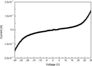
Fabricated devices are characterized using a Keithley (Cleveland, Ohio) 4200 semiconductor parameter analyzer. The dark current–voltage (I-V) characteristics are obtained for the applied voltage bias up to 30 V as shown in
Fig. 3. Devices exhibit dark current levels of 14 pA at
30 V bias, which show that the devices can be operated under a high reverse bias. The symmetric behavior of the
current–voltage curve is an indication of back-to-back
Schottky contacts.
Spectral photoresponsivity measurements are performed using a 150 W Xenon white light source and Newport Oriel (Irvine, California) 1/8 m Cornerstone monochromator. The incident monochromatic light is mechanically modu-lated using an optical chopper and the photogenerated electrical current is recorded with an SRS830 dual phase lock-in amplifier. The devices are illuminated from the top focusing the beam spot onto interdigitated electrodes.
A measured spectral photoresponsivity in the 200–500 nm
spectral range is shown in Fig. 4. The responsivity value decreases significantly at wavelengths larger than 300 nm due to the band edge of the HCPA-ALD-grown GaN film as verified by the previously reported optical characterization results.20,21 Fabricated devices show responsivity values of
1.687 and0.101 mA∕W at wavelengths of 200 and 390 nm,
respectively, under a 13 V reverse bias. Since the GaN films are deposited at temperatures below 200°C, these results signify the first demonstration of functional devices on such layers. The relatively low external quantum efficiency (ca
1%) is due to the low collection efficiency, which is attrib-uted to the nanocrystalline nature of the grown ALD GaN film. In ALD grown nanocrystalline GaN films, there are morphological imperfections such as nano-sized grains
with an average grain size of 9.3 nm.20 We believe that
grain boundary scattering reduces che arrier mobility, which results in low carrier collection efficiency. Moreover, nano-grains with varying crystal orientations may introduce addi-tional scattering. Overall, carrier collection efficiency is low due to such morphological and crystal imperfections that result in diminished carrier mobility. Devices exhibit a 15× UV/VIS rejection ratio based on photocurrent values at 200 nm (UV) and 390 nm (VIS). Photoresponsivity values increase with an applied reverse bias voltage. The photores-ponsivity value saturates for large reverse bias voltages (>10 V), which can be explained by the complete depletion of 20-nm-thick GaN film. The nonzero photoresponsivity at visible wavelengths (λ > 300 nm) is attributed to deep-level trap states within the forbidden gap that allow the absorption of sub-bandgap photons. The trap states are induced by crystal defects due to nitrogen interstitials.22,23 Nitrogen interstitials are believed to be responsible for acceptor-like
Fig. 1 (a) Schematic and (b) representative SEM image of fabricated GaN metal-semiconductor-metal (MSM) devices.
Fig. 2 Energy band diagram of the GaN metal-semiconductor-metal (MSM) photodetectors (PDs) (a) under thermal equilibrium, (b) with applied voltage bias, (c) under photoexcitation with applied voltage bias. Devices are illuminated from the top.
Fig. 3 GaN metal-semiconductor-metal (MSM) photodetector dark current-voltage characteristics.
Fig. 4 Spectral responsivity of the fabricated nanocrystalline-GaN (nc-GaN) metal-semiconductor-metal (MSM) photodetectors (PDs) for different applied voltage bias.
deep trap states.23 Furthermore, nitrogen-rich GaN favors negatively charged Ga vacancies, which introduce acceptor states as well.22 Such defect states promote a persistent
photoconductive gain that results in increased UV
photoresponse.
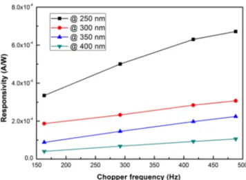
In addition, spectral photoresponsivity is investigated as a function of the chopper modulation frequency that is shown in Fig. 5. The photoresponse of the devices increases as chopper frequency increases. Trap states—mainly negatively charged Ga vacancies and nitrogen interstitials22,23–capture
electrons; however, these traps have long relaxation times,
i.e.,—electrons remain trapped while holes are mobile
longer. As a result, before relaxation occurs, holes continue to contribute to photocurrent. This phenomenon is known as persistent photoconductivity (PPC),22 resulting in a photo-conductive gain. For lower chopping frequencies, the time interval for no-illumination (dark time) is longer, therefore, more traps are relaxed and trapped electrons recombine with holes. As a result of reduced carriers, the gain due to PPC is reduced and the photocurrent decreases. When chopper frequency increases, less relaxation can occur due to shorter dark time intervals; as a result, electrons cannot recombine with holes and holes continue to circulate resulting in the persistent effect.
4 Conclusion
In summary, proof-of-principle MSM UV PDs are demon-strated for the first time using ultrathin nc-GaN layers depos-ited by HCPA-ALD at 200°C. These devices correspond to GaN-based PDs with the lowest thermal growth and fabrica-tion budget reported to date. The devices exhibit dark cur-rents of 3 pA under a 30 V reverse bias, which means they can operate under a high reverse bias. Spectral
photorespon-sivity measurements show a 15× UV/VIS rejection ratio
comparing 200 nm (UV) and 390 nm (VIS) wavelengths. The sub-bandgap photoresponse is attributed to deep-level traps in the forbidden gap. Persistent photoconductive gain is also shown to exist in PA-ALD grown GaN films. These results show the viability of UV photodetectors based on HCPA-ALD compatible with temperature sensitive and low cost substrates used for flexible and transparent electronics.
Acknowledgments
This work was performed at UNAM– Institute of Materials
Science and Nanotechnology, which is supported by the State Planning Organization of Turkey through the National Nanotechnology Research Center Project. This work was supported by the Scientific and Technological Research Council of Turkey (TUBITAK), (Grant Nos. 112M004, 112E052, 112M482 and 113M815). N. B. acknowledges support from European Union FP7 Marie Curie International Reintegration Grant (NEMSmart, Grant No. # PIRG05-GA-2009-249196). A. K. O. acknowledges a Marie Curie Inter-national Reintegration Grant (IRG). S. B. acknowledges TUBITAK-BIDEB for PhD fellowship, respectively. References
1. P. Peumans, A. Yakimov, and S. R. Forrest,“Small molecular weight organic thin-film photodetectors and solar cells,”J. Appl. Phys.93(7), 3693–3723 (2003).
2. S. Alkis et al.,“A plasmonic enhanced photodetector based on silicon nanocrystals obtained through laser ablation,”J. Opt.14(12), 125001– 125005 (2012).
3. S. Alkis et al.,“Thin film MoS2 nanocrystal based ultraviolet photo-detector,”Opt. Express20(19), 21815–21820 (2012).
4. B. Liu et al.,“ZnO-nanoparticle-assembled cloth for flexible photode-tectors and recyclable photocatalysts,”J. Mater. Chem.22(18), 9379– 9384 (2012).
5. H. Karaagac et al.,“A baseball-bat-like CdTe/TiO2 nanorods-based heterojunction core–shell solar cell,” J. Scripta Mat. 69(4), 323– 326 (2013).
6. W. Tian et al.,“Flexible ultraviolet photodetectors with broad photo-response based on branched ZnS-ZnO heterostructure nanofilms,” Adv. Mater.26(19), 3088–3093 (2014).
7. T. P. Chen et al.“Photoelectrical and low-frequency noise character-istics of ZnO nanorod photodetectors prepared on flexible substrate,” IEEE Trans. Electron. Devices 60(1), 229–234 (2013).
8. J. C. Carrano et al.,“Comprehensive characterization of metal-semi-conductor-metal ultraviolet photodetectors fabricated on single-crystal GaN,”J. Appl. Phys. Lett.83(11), 6148–6160 (1998).
9. A. Osinsky et al.,“Visible-blind GaN Schottky barrier detectors grown on Si(111),”J. Appl. Phys. Lett.72(5), 551–553, (1998).
10. N. Biyikli et al.,“High-speed visible-blind GaN-based indium–tin– oxide Schottky photodiodes,”Appl. Phys. Lett. 79(17), 2838–2840 (2001).
11. M. Mikulics et al.,“Ultrafast metal-semiconductor-metal photodetec-tors on low-temperature-grown GaN,” J. Appl. Phys. Lett. 86(21), 211110–211113 (2005).
12. H.Z. Xu et al.,“Fabrication and characterization of metal–semiconduc-tor–metal (MSM) ultraviolet photodetectors on undoped GaN/sapphire grown by MBE,”J. Cryst. Growth218(1), 1–6 (2000).
13. K. A. McIntosh et al.,“GaN avalanche photodiodes grown by hydride vapor-phase epitaxy,”J. Appl. Phys. Lett.75(22), 3485–3487 (1999). 14. E. C. Knox-Davies, J. M. Shannon, and S. R. P. Silva,“The properties and deposition process of GaN films grown by reactive sputtering at low temperatures,”J. Appl. Phys.99(17), 073503 (2006).
15. R. D. Vispute et al.,“Growth of epitaxial GaN films by pulsed laser deposition,”Appl. Phys. Lett.71(1), 102 (1997).
16. C. Ozgit et al.,“Self-limiting low-temperature growth of crystalline AlN thin films by plasma-enhanced atomic layer deposition,” Thin Solid Films520(7), 2750–2755 (2012).
17. N. El-Atab et al.,“Diode behavior in ultra-thin low temperature ALD grown zinc-oxide on silicon,”AIP Advances3(10), 102119–102126 (2013).
18. S. Alkis et al.,“UV/VIS range photodetectors based on thin film ALD grown ZnO/Si heterojunction diodes,”J. Opt.15(10), 105002–105006 (2013).
19. F. B. Oruc et al.,“Thin film ZnO charge trapping memory cell grown in a single ALD step,”IEEE Electon. Device Lett.33(12), 1714–1716 (2012).
20. C. Ozgit-Akgun et al.,“Hollow cathode plasma-assisted atomic layer deposition of crystalline AlN, GaN and AlxGa1-xN thin films at low temperatures,”J. Mater. Chem. C2(12), 2123–2136 (2014). 21. E. Goldenberg et al., “Optical characteristics of nanocrystalline
AlxGa1-xN thin films deposited by hollow cathode plasma-assisted atomic layer deposition,” J. Vac. Sci. Technol. A 32(3), 031508 (2014).
22. E. Muñoz et al.,“Photoconductor gain mechanisms in GaN ultraviolet detectors,”Appl. Phys. Lett.71(7), 870 (1997).
23. M. A. Reshchikov and H. Morkoc, “Luminescence properties of defects in GaN,”J. Appl. Phys.97(6), 061301–061396 (2005). Fig. 5 Responsivity values of the fabricated devices with respect to
Burak Tekcan received his BS degree in Electrical and Electronics Engineering from Bilkent University, Ankara, Turkey, in 2012. He is pursuing his MS degree in the Department of Electrical and Electrical Engineering at Bilkent University.
Cagla Ozgit-Akgun received her BS and MS degrees in metallurgical and materials engineering from Middle East Technical University, in 2006 and 2009, respectively, and her PhD degree in materials sci-ence and nanotechnology from Bilkent University in 2014. Currently, she is a postdoctoral researcher at Bilkent University UNAM-Institute of Material Science and Nanotechnology.
Sami Bolat received his BS degree in electrical and electronics engi-neering from Middle East Technical University, Ankara, Turkey, in 2012. He received his MS degree in electrical and electronics engi-neering from Bilkent University, Ankara, Turkey, in 2014. Currently, he is a teaching and research assistant in the Department of Electrical and Electronics Engineering at Bilkent University, where he is also pursuing his PhD degree.
Necmi Biyikli received his BS, MS, and PhD degrees in electrical and electronics engineering from Bilkent University, Ankara, Turkey, in 1996, 1998, and 2004, respectively. After postdoctoral research at the Virginia Commonwealth University and Cornell Nanoscale Science and Technology Facility (CNF), in 2008, he joined the National Nanotechnology Research Center (UNAM) and Materials Science & Nanotechnology Institute at Bilkent University where he currently leads the“Functional Semiconductor Materials and Devices Laboratory.”
Ali Kemal Okyay received his BS degree in electrical and electronics engineering from Middle East Technical University, in 2001 and his MS and PhD degrees in electrical engineering from Stanford Univer-sity, CA, in 2003 and 2007, respectively. Since January 2008, he has been working as a faculty member at Bilkent University, where he presently holds joint appointments as an assistant professor in the Electrical and Electronics Engineering Department, and the Institute of Material Science and Nanotechnology.