NOVEL PLASMONIC DEVICES
FOR
NANO-PHOTONICS APPLICATIONS
A DISSERTATION
SUBMITTED TO THE DEPARTMENT OF ELECTRICAL AND ELECTRONICS ENGINEERING AND GRADUATE SCHOOL OF
ENGINEERING AND SCIENCE OF BILKENT UNIVERSITY
IN PARTIAL FULFILLMENT OF THE REQUIREMENTS FOR THE DEGREE OF
DOCTOR OF PHILOSOPHY
By Levent Şahin
I certify that I have read this thesis and that in my opinion it is fully adequate, in scope and in quality, as a dissertation for the degree of Doctor of Philosophy.
Prof. Dr. Ekmel Özbay (Supervisor)
I certify that I have read this thesis and that in my opinion it is fully adequate, in scope and in quality, as a dissertation for the degree of Doctor of Philosophy.
Prof. Dr. Gönül Turhan Sayan
I certify that I have read this thesis and that in my opinion it is fully adequate, in scope and in quality, as a dissertation for the degree of Doctor of Philosophy.
I certify that I have read this thesis and that in my opinion it is fully adequate, in scope and in quality, as a dissertation for the degree of Doctor of Philosophy.
Prof. Dr. Oğuz Gülseren
I certify that I have read this thesis and that in my opinion it is fully adequate, in scope and in quality, as a dissertation for the degree of Doctor of Philosophy.
Assoc. Prof. Dr. Vakur B. Ertürk
Approved for the Graduate School of Engineering and Science:
Prof. Dr. Levent Onural Director of the Graduate School
ABSTRACT
NOVEL PLASMONIC DEVICES FOR NANO-PHOTONICS
APPLICATIONS
Levent Şahin
Ph.D. in Electrical and Electronics Engineering Supervisor: Prof. Dr. Ekmel Özbay
July, 2013
Plasmonics have attracted a great deal of interest because of their potential to design novel photonics devices which have unique optical properties. This dissertation focuses on novel plasmonic device designs for photonics applications.
Electromagnetic properties of metamaterials are characterized and the resonance mechanism of Split Ring Resonator (SRR) structure is investigated. Furthermore, novel SRR-based metamaterial structures are studied. We demonstrated the significant plasmonic enhancement in the transmission characteristics through a sub-wavelength aperture by utilizing SRR resonances.
Electrical tuning of plasmonic resonance with varying gate bias by using graphene is observed. Also, electrical properties of graphene is investigated. Fabrication of electrically gated graphene based plasmonic structures are realized. In addition, we utilized metamaterials to design novel photonic devices and we experimentally studied and numerically
verified the novel propagation characteristics of graphene-based photonic devices and 3D nanostructures. The proposed structures are designed, simulated, fabricated and measured. The simulations and experimental results are in good agreement and shows significant enhancement of transmission characteristics of plasmonic devices. The dimensions of the structures that are designed in our work is less than 10 times smaller than the incident wavelength (r/λ~0.1) which is a desired property for enhanced light confinement of sensors. Also, the gate tuning of SRR's plasmonic resonance is the first demonstration in the contemporary literature according to our knowledge.
Keywords: Plasmonics, Photonics, Metamaterial, Split Ring Resonator (SRR) Structure, Graphene, Tunable Resonances, 3D Direct Writing, Enhanced Transmission, Sub-wavelength Aperture
ÖZET
NANO-FOTONİK UYGULAMALAR İÇİN YENİ
PLAZMONİK CİHAZLAR
Levent Şahin
Elektrik ve Elektronik Mühendisliği, Doktora Tez Yöneticisi: Prof. Dr. Ekmel Özbay
Temmuz, 2013
Plazmonik kendine has optik özellikleri olan yeni fotonik cihazların geliştirilmesindeki potansiyeli nedeniyle büyük ilgi çekmektedir. Bu Tez, fotonik uygulamalar için yeni plazmonik cihaz tasarımlarına odaklanmaktadır.
Metamalzemelerin elektromanyetik özellikleri tanımlanmakta ve Yarıklı Halka Rezonatörü (YHR) yapısının rezonans mekanizması incelenmektedir. Bunun yanında, YHR temelli yen metamalzeme yapıları çalışılmıştır. YHR rezonanslarından faydalanarak dalga boyu altı aralıktan plazmonik geçirgenlikte önemli oranda artış gözlemlendi.
Grafen kullanarak plazmonik rezonansın değişken geçit meyili ile elektriksel ayarlanması gözlemlendi. Aynı zamanda, grafenin elektriksel özellikleri incelendi. Elektriksel geçitli grafen temelli plazmonik yapılar gerçekleştirildi. Ayrıca, yeni fotonik cihazların tasarımı için metamalzemeler kullanıldı ve grafen temelli fotonik cihazlar ile 3B nanoyapıların yeni yayılma özellikleri deneysel olarak çalışıldı ve benzetim ile doğrulandı. Önerilen yapılar tasarlandı, benzetim yapıldı,
üretildi ve ölçüldü. Benzetim çalışmaları ve ölçümler benzer sonuçlar verdi ve önerilen yeni yapıların kullanılması ile plazmonik cihazların geçirgenlik özelliklerinde önemli oranda artış gözlemlendi. Çalışmamızda tasarlanan yapıların boyutları gelen dalganın dalga boyundan 10 kat (r/λ~0.1) daha küçüktür ve bu sensorler için gereken artırılmış ışık toplanması amacıyla istenmektedir. Ayrıca, çalışmamızdaki YHR'nin plazmonik rezonansının geçit ayarlanması bildiğimiz kadarıyla güncel literatürdeki ilk gösterimdir.
Anahtar Sözcükler: Plazmonik, Fotonik, Metamalzeme, Yarıklı Halka Rezonatörü
Yapısı, Grafen, Ayarlanabilen Resonanslar, 3B Doğrudan Yazım, Artırılmış Geçirgenlik, Dalga Boyu Altı Aralık
ACKNOWLEDGEMENT
I would like to express my sincere gratitude to my thesis supervisor Prof. Ekmel Özbay for his invaluable guidance and motivation. His support, encouragements and suggestions taught me much about systematically approaching to research study. I am grateful to Nanotechnology Research Center (NANOTAM) for the facilities and working environment provided for me to perform the research study.
I would like to thank to the members of my thesis committee, Prof. Dr. Gönül Turhan-Sayan, Prof. Dr. Orhan Aytür, Prof. Dr. Oğuz Gülseren and Assoc. Prof. Dr. Vakur B. Ertürk for reading the manuscript and commenting on the dissertation.
Special thanks and gratitude to Prof. Dr. Eric Mazur who supervised my research work at Harvard University while I was a visiting scientist. His research group provided support, encouragement and valuable ideas towards the realization some of the research work presented in this dissertation. Special thanks to my friend Dr. Kevin Vora for his support during my research work at Harvard.
During my dissertation work, I had the opportunity to work with a number of collaborators. I would like to thank to Kevin Vora, Phillip Munoz, Erdem Demircioğlu, A. Burak Turhan, Yasemin Kanlı and Semih Çakmakyapan for discussions on various aspects of research study.
I would like to thank Republic of Turkey, Prime Ministry (PM) for the permission to the study on the dissertation. Also, my special thanks to Dr. Orhan Şengül for his continuous support and encouragement. I would like to thank TÜBITAK - BİDEB (The Scientific and Technological Research Council of Turkey - The Department of Science Fellowships and Grant Programmes) for their support during my dissertation.
Last but not the least; I would present my endless thanks to my parents, Şaziye and Sayit Şahin; and to my beloved wife Dr. Fatma Başıbüyük-Şahin for their endless support, encouragement and love. This dissertation could not be completed without their support. I dedicate this labor to my son, the newest member of my family. He came into our life during the final stage of my Ph.D. study and helped me to overcome any worries and trouble.
CONTENTS
1. Introduction ... 1
1.1 Motivation ... 1
1.2 Outline of the thesis ... 5
2. Metamaterial based Plasmonics ... 7
2.1. Introduction ... 7
2.2. Metamaterials ... 11
2.3. Split-Ring Resonator (SRR) Structures ... 27
2.4. Plasmonic Enhancement of Light/Wave ... 35
2.4. Summary ... 75
3. Graphene Based Metamaterials ... 76
3.1. Introduction ... 76
3.2. Electrical Gate Tuning ... 79
3.3. Design, Fabrication and Electrical Gating... 95
3.4. Results ... 103
3.5 Summary ... 106
4. Three Dimensional Nanostructures ... 108
4.1. Introduction ... 108
4.2 Femto-second Laser Writing ... 109
4.3 Random Alignment, Random Radius Silver Nanodots ... 114
4.4 Summary ... 124
5. Conclusions and Future Work ... 125
List of Figures
Figure 2.1: Development of metal-based metamaterial as a function of operation frequency and time.. ... 8 Figure 2.2: Potential applications such as subdiffraction imaging, sensing, cloaking ... 9 Figure 2.3: The schematic representation of a periodic metallic wire array. a is the lattice constant and r is radius of a single wire. ... 18 Figure 2.4:
µ
eff -w diagram for ideal single SRR structure. ... 21 Figure 2.5: Negative refraction of electromagnetic wave through a left-handed medium. ... 24 Figure 2.6: Progress made in scaling metamaterials from microwave to optical frequencies. ... 25 Figure 2.7: Schematics of a) single SRR b) periodic arrangement of SRR array (microwave and optical replica). ... 28 Figure 2.8: Schematic Representation of an SRR a) SRR structures modeled at Lumerical. w: width of metal, d: gap distance, t: gap between two concentric rings, h: thickness of metal. ... 30 Figure 2.9: Single ring SRR structure modeled at Lumerical. w: width of metal, d: gap distance, h: thickness of metal. ... 32 Figure 2.10: Simulation Results of SRR (l=200 nm, w=d=h 50 nm). ... 33 Figure 2.11: Simulation results of a SRR and CSRR structures. CSRR structure is depicted in the inset CSRR (l=200 nm, w=h= 50 nm). ... 34Figure 2.12: Theoretical suggestion of Bethe (λ−4
decrease) and the simulation
results of transmission through a sub-wavelength aperture where r<λ10. ... 37
Figure 2.13: Transmission through a sub-wavelength aperture[23]. ... 38
Figure 2.14: Schematic representations of SRR devices for a) Microwave Regime b) Optical Regime. ... 40
Figure 2.15: Schematic drawing of Split Ring Resonator structure used for microwave. ... 43
Figure 2.16: a) Transmission spectrum of optimized version of proposed structure (inset is a) the schematic of optimum alignment) b) enhancement spectrum. ... 45
Figure 2.17: Experimental setup used in measurements. ... 47
Figure 2.18: a) Transmission spectrum, b) Enhancement spectrum. ... 48
Figure 2.19: Schematic Representation of SRR coupling aperture. ... 50
Figure 2.20: Suggested SRR coupling structure. ... 52
Figure 2.21: a) Transmission spectrum of the SRR-coupled aperture structure and a single aperture. b) Enhancement spectrum - Simulation Results... 53
Figure 2.22: SRR structure. ... 59
Figure 2.23: a) Schematic representation of SRR b) Transmission (S21) and reflection (S11) spectra of the SRR structure [8]. ... 60
Figure 2.24: Schematic representation of the SRR-shaped aperture model (Gray parts are the metal plate and the blue parts are the gaps). ... 61
Figure 2.25: a) The calculated transmission spectrum of the SRR-shaped structure and a single aperture. b) Enhancement spectrum. ... 62
Figure 2.26: a) Schematic representation of the Closed Ring Resonator (CRR) shaped aperture. b) Transmission spectrum of the CRR-shaped aperture and the SRR-shaped aperture. ... 64
Figure 2.27: The schematics of the proposed SRR-shaped aperture structures. .. 65
Figure 2.28: Transmission and enhancement spectrum of the proposed SRR-shaped apertures - Measured & calculated. ... 67
Figure 2.30: a) Transmission spectrum of the SRR-shaped structure and a single aperture. b) The enhancement spectrum (l=200 nm, w=h= 50 nm, d:100nm). -
Simulation Results. ... 72
Figure 2.31: Simulation results of a SRR and CSRR structures. CSRR structure is depicted in the inset CSRR (l=200 nm, w=h= 50 nm), a) Transmission, b) Enhancement. ... 73
Figure 3.1: Permittivity of graphene obtained by RPA at 300K: a) real b) imaginary. ... 88
Figure 3.2: SRR model. ... 91
Figure 3.3: SRR and SRR-SiO2-Si spectrum. ... 92
Figure 3.4: a) Schematic of graphene hybrid SRR structure, b) Device Configuration. ... 93
Figure 3.5: Simulated transmission spectra for different gate voltages and corresponding charge carrier concentrations. ... 94
Figure 3.5 Graphene. ... 95
Figure 3.6 Van der Pauw device for Hall measurements. ... 96
Figure 3.7: Ohmic contacts and alignment marks. ... 97
Figure 3.8: Mesa etching of active region. ... 97
Figure 3.9: SRR fabrication. ... 98
Figure 3.10: Interconnect metallization... 99
Figure 3.11: Gate Deposition. ... 99
Figure 3.12: Gate interconnect deposition. ... 100
Figure 3.13: Fabricated SRR-graphene hybrid Structures. ... 101
Figure 3.14: Fabricated SRR and SRR+graphene Structures. ... 102
Figure 3.15: DC IV measurement... 103
Figure 3.16: a) Measured optical transmission spectra of SRR strcutures for different gate voltages (Inset is zoomed graph). b) Simulated transmission spectra for different gate voltages and corresponding charge carrier concentrations. ... 104
Figure 4.1: 3D patterns composed of (a) dielectric spheres and (b) metallic
spheres . ... 110
Figure 4.2: Schematic of the fabrication process [208]. ... 112
Figure 4.3: Material Schematic. ... 113
Figure 4.4: TEM image of fabricated silver nanodots. ... 113
Figure 4.5: Diffraction experiment by shining a laser beam to the square lattice pattern. ... 114
Figure 4.6: Random silver nanodots radius ranging from 3 nm to 10 nm. ... 115
Figure 4.7: Real part of refractive index... 118
Figure 4.8: Real part of permittivity. ... 119
Figure 4.9: Real part of permeability. ... 120
Figure 4.10: Imaginary part of refractive index. ... 121
Figure 4.11: Imaginary part of permittivity. ... 122
List of Tables
Table 3.1: Numerical results of resonances tuning for different gate voltages....94 Table 3.2: Resonances for different gate voltages (Sim. and Exp.)...105
Chapter 1
Introduction
1.1 Motivation
Plasmonics is a growing new research field of science as a result of unique optical properties of metallic nanostructures that can be utilized to manipulate transmission and propagation characteristics of light. Nanometallic structures' optical properties stem from the ability to support collective electron excitations which is called plasmons.
Plasmons are defined as the coupled electromagnetic waves which propagates through its path between a metal and a dielectric interface. The increasing interest on plasmons stem from ability to confine light to nanoscale regions which can be much smaller than the wavelength of light. Therefore, plasmonics can provide nanoscale confinement and localization which is related to coupling of surface plasmons and waveguiding, and active functionality on the nanoscale.
Light can couple the free-electron excitations near the metallic surfaces as a result of its interaction with metal nanostructures. Surface plasmon-related electromagnetic resonances are plasmon-related to surface details of the nanostructure which creates significant novel research areas for control of light. The control of light opens up significant opportunities for scientist to design plasmonic devices which are candidates to solve contemporary engineering challenges. In addition to providing novel devices, plasmonic devices lead to scaling down the sizes of optical devices and components. On the other hand, there are several challenges to overcome. The most prominent one is the Ohmic losses which impose fundamental constraint at optical frequencies. Also fabrication at nanoscale accuracy is a problem. We cannot control the geometry well without nanoscale precision at fabrication.
Metamaterial based plasmonic devices are prominent candidates for designing novel optical devices. Therefore, we will investigate the metamaterial based photonic devices in our dissertation.
Metamaterials have shown significant potential in recent years due to their scientific-breakthrough properties and applications to create novel devices that exhibit specific electromagnetic properties. The main idea behind the metamaterials is to manipulate constitutive parameters of artificially designed materials to obtain peculiar electromagnetic properties.
Since, response of materials to an incident electromagnetic wave is determined by their constitutive macroscopic electromagnetic parameters, the dielectric permittivity (ε) and magnetic permeability (μ), we can design artificial materials that respond to incident electromagnetic
waves in a desired characteristics. Ordinary materials generally have positive ε and μ, which restrict the design of novel devices. However, new structures called metamaterials are proposed for realizing novel response characteristics that do not occur in nature. The phrase “meta” means “beyond” in Greek, which refers the novel electromagnetic characteristics of metamaterials that are not available in nature. The engineered response of metamaterials has the potential to make a dramatic impact on the design of novel electromagnetic devices; as they provide the possibility to achieve novel physical phenomena that cannot be achieved with conventional, naturally occurring materials.
V. Veselago was the first scientist who theoretically suggested metamaterials with simultaneously negative dielectric permittivity and magnetic permeability at 1968 [1]. After a long time later, increasing interest in this topic started by the seminal works of J.B. Pendry et al. [2] and D.R. Smith et al. [3]. Since metamaterials offer new physical phenomena, there is an increasing amount of interest and a large amount of literature has been accumulated on metamaterials [4-16]. Also novel applications such as superlenses [17, 18], enhanced magnetic resonance imaging [18], hyperlenses [20, 21], cloaking [22], and semiconductor metamaterials [23] are achieved.
At the beginning, the research activities of metamaterial based photonics were mainly focused on obtaining artificial materials with negative permeability and negative index properties. However, new research fields for the applications of metamaterials have emerged lately. These research fields are mostly related to the transmission and propagation properties of novel structures.
In addition, there are wide varieties of study on metamaterials to change the transmission characteristics of several structures, which are restricted to several physical restrictions that cannot be overcome by ordinary materials. Transmission through a sub-wavelength hole is another contemporary research topic because of its applications of critical importance ranging from biomaterials to microscopy. The last century concluded with a very important discovery by Ebbesen [24]; sub-wavelength holes in a thin metal film can transmit electromagnetic waves much more strongly at certain frequencies than the Bethe’s prediction [25] by utilizing hole arrays. Ebbesen’s discovery (extraordinary transmission phenomenon) and new fabrication techniques opened up significant opportunities to design novel devices.
Also we studied graphene-based photonic devices. Graphene is an extraordinary material which is believed to have outstanding applications in photonics. Therefore, design of graphene-based novel photonic systems is an active research field. However, exciting opportunity to design novel photonic devices using graphene structures has not been fully exploited. Electrical tuning of plasmonic resonance with varying gate bias by using graphene is observed.
In the present dissertation, we investigated the transmission and propagation properties of metamaterials. We utilized metamaterials to design novel photonic devices and we experimentally studied and numerically verified the novel propagation characteristics of graphene-based photonic devices and 3D nanostructures.
1.2 Outline of the thesis
This dissertation is organized into 5 chapters. We investigated novel plasmonic devices for nano-photonics applications. We experimentally studied and numerically verified the propagation characteristics of novel plasmonic devices. Besides this introductory chapter which is aimed to provided a brief introduction of the dissertation, the content of the chapters are organized as follows:
In Chapter 2, the metamaterial based plasmonics is introduced and design of novel devices are investigated. Several novel structures to increase the transmission through a sub-wavelength aperture is investigated. The negative dielectric permittivity and negative magnetic permeability phenomenon are discussed. In addition, the negative index of refraction of left-handed metamaterials is demonstrated.
Chapter 3 is about the Nobel-winning graphene material's possible applications on photonics. Several novel structures to utilize promising properties of graphene is investigated. Finally, electrical tuning of plasmonic resonance by using graphene is observed with varying gate bias. This effect is studied with theoretical modeling and confirmed experimentally.
Chapter 4 is devoted to 3D nanostructures fabricated with femto-second laser writing which can be a base for new optical devices. Measurements and simulations are performed in order to observe 3D fabrication.
Furthermore, refractive index increase with increasing filling factor of FCC lattice is verified by using the retrieval procedure.
Finally, Chapter 5 provides a concise summary of the work presented in this dissertation Moreover, the future research directions and future work are provided in this chapter.
Chapter 2
Metamaterial based Plasmonics
2.1. Introduction
Metamaterials are artificially made structures with tailored sub-wavelength unit cells. They emerged with new and unusual properties which were previously unattainable in natural materials.
Over the past eight years, metamaterials have shown tremendous potential in many disciplines of science and technology. First designs were microwave devices that proved the concept. After that, operating frequency of metamaterials increased over the years [26]. This tremendous increase in operation frequency is a result of miniaturizing SRR devices. Challenging the limitations arising from scaling of microwave metamaterial designs to optical frequencies is one of the major research area of plasmonics nowadays. Because, optical metamaterials opens up significant opportunities to design an entire new generation of miniaturized passive and active optical elements.
Figure 2.1: Development of metal-based metamaterial as a function of operation
frequency and time. Orange: double SRRs; purple: transmission-Line structures [29], copyright (2004) by the American Physical Society; green: U-shaped SRRs; blue: metallic
cut-wire pairs; red: double fishnet structures. The five insets show optical or electron micrographs of the five kinds of structure. Reprinted by permission from Macmillan
Publishers Ltd: [Nature Photonics] [12].
Metamaterials design started with the design of first negative permittivity devices, thin metal wires. After that SRRs are suggested by Pendry et. al. to demonstrate negative permeability [2]. Obtaining both negative permittivity and permeability paved the wave of negative refractive index. Negative refractive index phenomenon created new opportunities to design novel devices especially at optical regime. Therefore, microwave devices are scaled down to obtain optical devices. However, fabrication of optical metamaterials and loss issues is still a challenge for researchers.
Main drawbacks of metal-based metamaterials, which are need to be overcome, are conduction loss and anisotropy [26].
Figure 2.2: Potential applications such as subdiffraction imaging, sensing, cloaking [36].
Metamaterials are the pioneer devices of compact and novel photonic devices [27]. Artificially designed metamaterials are proposed to mimic bulk materials [3]. Since, we can design each elements in a bulk metamaterial, we can design frequency response of the metamaterial which is not available property of natural materials. Moreover, we can modulate the spectral response by including active elements. [12].
Unit cell of metamaterial is at the scale of sub-wavelength. Therefore, ultra compact photonic devices which are only several wavelengths in footprint is a possibility. Plasmonic resonance which emanates from metallic ring of SRR at optical regime is the driving force for optical metamaterial. Plasmons created by the SRR's metallic ring accumulated at
resonance frequency and creates high spatial field density which makes novel metamaterial-based devices possible.
Plasmons are defined as the coupled electromagnetic waves which exists between a metal and a dielectric interface. The increasing interest on plasmons stem from ability to confine light to nanoscale regions which can be much smaller than the wavelength of light. Therefore, plasmonics can provide nanoscale confinement and localization which is related to coupling of surface plasmons and waveguiding, and active functionality on the nanoscale. Plasmonic spatial localization and high density of states is superior to other methods on the same scale [30].
Light can couple the free-electron excitations near the metallic surfaces as a result of its interaction with metal nanostructures. Surface plasmon-related electromagnetic resonances are plasmon-related to surface details of the nanostructure which creates novel research paths for control of light. The control of light opens up significant opportunities for scientist to design plasmonic devices which are candidates to solve contemporary engineering challenges. In addition to providing novel devices, plasmonic devices lead to scaling down the sizes of optical devices and components. On the other hand, there are several challenges to overcome. The most prominent one is the Ohmic losses which impose fundamental constraint at optical frequencies. Also fabrication at nanoscale accuracy is a problem. We cannot control the geometry well without nanoscale precision at fabrication.
In this section, we demonstrate metamaterial based plasmonic devices operating at microwave and optical frequencies. Resonance characteristic
of SRR is investigated for both microwave and light. Also the effect of geometrical parameters on the resonance of SRR is discussed. We made several transmission measurements and simulations; and observed enhanced transmission over a common frequency range.
2.2.
Metamaterials
Metamaterials are the artificial structured materials which have unique properties to interact with waves that are not usually found in nature. Development of artificial dielectric media which are used for designing metamaterials has become a remarkable research area due to its potential for creating new devices that exhibit unusual electromagnetic properties [36]. The applications of novel dielectric media in various areas such as imaging, lensing, optical fibers, and lasers require the effective control of the transmission and propagation of electromagnetic waves. As we control permittivity and permeability values of a structure, we can design metamaterials. The metamaterial's constitutive parameters (ε,μ) can be determined to a desired value which are great candidates to be used in several applications ranging from focusing without a diffraction limit to extraordinary transmission through sub-wavelength apertures.
Electromagnetic response of materials is determined by the fundamental constitutive parameters, the dielectric permittivity (ε), the magnetic permeability (μ) and the conductivity (σ). The combined effect of permittivity and permeability determine the response of a lossless material to an incident electromagnetic field. Most of the natural structures have positive permittivity and permeability. Due to the absence of magnetic charges, it is rather difficult to have negative
permeability structures, while negative permittivity is obtained below the plasma frequency of periodic sub-wavelength metallic wires at microwave frequencies as shown theoretically [39, 40] and experimentally [41]. The phenomenon of negative refraction of electromagnetic wave in media with negative permittivity and permeability was first suggested by Vesalago in 1968 [1]. A material that has both negative permittivity and permeability was predicted to have negative refractive index, the reversal of Doppler Effect [1, 51] and Cerenkov radiation [52]. Materials with negative index of refraction (n<0) demonstrate the unusual behavior that the propagation direction of electromagnetic wave is opposite to the direction of the energy flow. In other words, the phase velocity and group velocity are antiparallel, which is an extraordinary behavior of left-handed materials that may open up significant opportunities to develop novel electromagnetic devices.
Negative permittivity is demonstrated by utilizing periodic metallic wire arrangements at the microwave regime [39-41]. Dielectric permittivity is negative below the plasma frequency of a metallic wire array and no electromagnetic wave can propagate at the negative permittivity spectrum as long as the permeability remains positive. No material with negative permeability was suggested until the seminal work of Pendry et al. [2], where a periodic arrangement of novel resonator structures called Split Ring Resonators (SRRs) was employed to obtain negative permeability around the resonance frequency. Afterwards, Smith et al. experimentally demonstrated a novel type of materials, composite metamaterials, by stacking thin wires and SRRs [3, 45] so that left-handed propagation band was observed at frequencies where both the dielectric
permittivity and magnetic permeability of this composite metamaterial were both negative.
Negative index of refraction is theoretically [1, 46] and experimentally [47] verified where both permittivity and permeability are both negative. Negative index of refraction for left-handed materials has been confirmed in agreement with various other studies [46-50, 53].
The fundamental postulate for the large-scale (macroscopic) electromagnetic phenomena is described by Maxwell’s Equations. Therefore, the theoretical analysis of metamaterials starts with Maxwell’s Equations.
Electromagnetic field solutions at every point in space must satisfy the Maxwell’s Equations which are expressed in time domain as follows:
t B E ∂ ∂ − = ×
∇ (Faraday’s Induction Law) (2.1)
J t D H + ∂ ∂ = × ∇
(Generalized Ampere’s Circuital Law) (2.2)
ρ
= • ∇ D (Gauss’ Law) (2.3) 0 = •∇ B (Conservation of Magnetic Flux) (2.4)
Also, the mathematical statement of “conservation of electric charge” is given by the Continuity Equation:
t J ∂ ∂ − = • ∇ ρ (2.5)
which is linearly dependent on Maxwell’s Equations.
The vector and scalar quantities in Eqn. 2.1 through Eqn. 2.5 are functions of both space variables and time.
We considered the uniform plane wave excitation at a given angular frequency w for the simplicity of our analysis. Using the jwt
e+ convention, the mathematical expressions for the E and H fields of a uniform plane wave in phasor domain can be given as
r k j e E E = 0 + • (2.6.a) r k j e H H = 0 + • (2.6.b)
where k is the propagation vector, r is the position vector and the wave is assumed to propagate in a simple (linear, homogeneous and isotropic), lossless and source-free media with constitutive relations
H
B=
µ
(2.7.a)E
D=ε (2.7.a)
The reduced Maxwell’s equations for monochromatic, isotropic plane wave can be derived in phasor domain as;
H w E k× =−
µ
(2.8) E w H k× = ε (2.9)Moreover, the simplest dispersion relation for the isotropic, homogeneous and lossless materials can be derived as:
0
2 2−
µε
=
w
k
(2.10.a) 2 2 2 n w k = (2.10.b)where n, the refractive index of the medium, is given by
n=
µ
ε
(2.11.a)or, for a composite medium with effective medium parameters
µ
eff and effε
, given byeff eff
n = µ ε (2.11.b)
The dispersion relation (Eqn. 2.10.a) is the equation defines the propagation of wave. As we can see, ε and μ are the only material properties in Eq. 2.10.a. Therefore, we can state that the dielectric permittivity (ε) and magnetic permeability (μ) of a material are the characteristic parameters of the material for a lossless media. On the other hand, Eqn. 2.10.b states that as both ε and μ become negative, the refractive index (n) does not change its sign; however, the Maxwell’s relations show the effect of simultaneous negative dielectric permittivity and magnetic permeability. The materials with simultaneous negative ε and μ exhibit unique properties that are different from ordinary positive ε and μ materials [1].
As can be seen in Eqns. (2.8) and (2.9), { E , H , k } form a right-handed orthogonal coordinate system for materials with positive ε and μ. In case both ε and μ are negative, an interesting result arises; { E , H ,- k } forms a left-handed orthogonal coordinate system.
In addition, since the sign of Poynting Vector ( P ) is independent of the sign of ε and μ (Eqn. 2.12), the direction of the energy flow does not change:
H E × =
Ρ (2.12)
Therefore, the direction of the power flow never changes. However, the wave propagation direction is opposite to the direction of power flow in left-handed metamaterials. In other words, this result causes the famous effect of an antiparellel phase and group velocity, the reversal of the Doppler Shift [51], and Cerenkov radiation [52].
For materials with negative ε and positive μ or vice versa. Electromagnetic waves become evanescent as a result of imaginary propagation constant (k). When, both ε and μ are negative, the wave can propagate as a result of εμ>0 (real propagation constant, k). So far, we analyzed the situation when ε and μ are both positive and negative. If the signs of ε and μ are opposite (εμ<0), then the electromagnetic waves are reflected totally and evanescent waves occur. Also the reflection is reversed and the exciting new phenomena occurs with these kind of materials.
Transmission properties of a lossless (or very low loss) material are determined by its dielectric permittivity and magnetic permeability.
Therefore, we firstly investigate the phenomenon of negative permittivity. Then, the negative permeability phenomenon and negative index metamaterials which possess both negative permittivity and negative permeability will be investigated.
2.2.1. Negative Permittivity
Negative dielectric permittivity is dominant for metals at optical frequencies as a result of the plasma frequency of metals. Under a specific frequency called plasma frequency, the real part of permittivity parameter of a plasma medium is negative. However, it is hard to have negative dielectric permittivity at lower frequencies, such as near infrared and the microwave regime; because, the dissipation dominates in metallic media as a result of significant increase in the dissipation of the plasmon’s energy in the system [40-41]. Therefore, the dielectric permittivity becomes purely imaginary. In 1996, Pendry et al. proposed the arrangement of periodic metal wires for the depression of the plasma frequency into the near infrared and GHz band [39]. The physical mechanism behind Pendry et al.’s suggestion is the confinement of electrons into thin wires for enhancing the effective electron mass through self-inductance. Therefore, the proposed structure has negative permittivity at microwave frequencies by using suitable parameters. The plasma frequency of the periodic thin wire array is given by making detailed analytical derivations as follows [39]:
r a a c m e n w eff eff p ln 2 2 2 0 0 2 2 ⋅ ⋅ = ⋅ ⋅ =
π
ε
(2.13)where,
c
0 is the speed of light, a is the lattice parameter and r is theradius of each wire (see Figure 2.3).
Figure 2.3: The schematic representation of a periodic metallic wire array. a is the lattice
constant and r is radius of a single wire.
Eqn. 2.13 states the fact that the plasma frequency can be expressed in terms of the macroscopic parameters of the array structure (a, r) instead of the microscopic quantities (effective electron mass-meff, effective electron density-neff ). Moreover, the parameters of the metallic wire array lattice (a, r) are much smaller than the wavelength. When all the lattice parameters (a, r) of the thin metallic wires are much smaller than the wavelength (a<<λ, r<<λ), the response of the wire array can be interpreted by the effective medium theory. Therefore, an effective dielectric permittivity (
ε
eff ) can be used to define the dielectric permittivity parameter of the material/medium. In other words, the periodic array of metallic wires appears to be an effective homogeneous material having an effective dielectric permittivity with negative real part.We calculated the plasma frequency of various fictitious thin wire arrays and made simulations in before [38] in order to confirm the theoretical expectations.
The model of Pendry et al. was further improved in various other studies [3]. Different approaches such as the one which models a periodic metallic wire array by using circuit models have been proposed [55]. We used the abovementioned model for microwave devices. On the other hand, we used the plasma frequency parameter of metals for optical simulations.
2.2.2. Negative Permeability
Designing a material with negative permeability is much more difficult than designing one with negative dielectric permittivity. The lack of a magnetic charge in nature is the main reason behind the difficulty of obtaining negative permeability materials. Since the magnetic response of natural materials is not strong at microwave frequencies, the magnetic moment of atom or molecules cannot be utilized effectively. Therefore, we need to have a strong magnetic dipole moment effect obtained artificially. In 1999, Pendry et al. suggested several types of periodically arranged resonator structures that give strong enough magnetic response to an incident electromagnetic field [2].
The periodic thin wire array that was mentioned in the previous chapter responds to an incident electromagnetic field such that the effective dielectric permittivity of the structure becomes negative below the plasma frequency, but its permeability remains positive. Since, a magnetic dipole moment can be created by a current carrying conductor loop; a metallic ring structure provides a suitable structure to obtain a strong magnetic response. However, the rings should also have capacitive elements such as splits in order to be resonant at wavelengths much
larger than the diameter of the rings. Also, the structures are periodic arrangements of arrays in order to couple each other and increase the magnetic resonance. The strong magnetic resonance gives rise to negative permeability over a narrow resonance band.
The widely used structure for having negative permeability at microwaves is a Split Ring Resonator (SRR) structure [2] which is composed of two conducting rings with splits where the split locations are 180 degrees apart from each other. The splits are used to make the SRR resonant at wavelength much larger than the diameter of the SRR. The gap between the rings, splits, and inner split ring are all used to increase the capacitance that enables a decrease in the resonance frequency of the structure. If the largest dimension of the SRR is much smaller than the wavelength of the resonance frequency, the response of a periodic arrangement of the SRR array can be analyzed by the effective medium theory such as we have mentioned in the case of the thin wire array. Therefore, an effective magnetic permeability (
µ
eff) can be used to define the permeability parameter of the resulting material/medium.The critical frequencies and effective permeability (
µ
eff) for the SRR structure are analytically derived as [2]:3 2 2 2 2 1 3 r a r c d wmp ⋅ − ⋅ ⋅ ⋅ =
π
π
(2.17) 3 2 2 0 3 r c d w ⋅ ⋅ ⋅ =π
(2.18)2 3 2 2 0 2 2 3 2 1 1 w r dc wr j a r eff π µ σ π µ − ⋅ + ⋅ − = (2.19)
where, c is the speed of light in vacuum, a is the lattice constant for a unit cell,
µ
0 is the magnetic permeability constant of vacuum, r is the radius ofthe inner ring and σ is the conductivity of the cylinder surface per unit area.
The capacitance introduced into the system by the splits and the gap between the rings collaborates with the inductance introduced into the system by the metallic rings in order to resonate. Figure 2.6 shows the typical
µ
eff form of a SRR as a function of angular frequency w under the assumption that the metallic rings are made of a perfect electric conductor (PEC) [2]:SRR's negative permeability is not very effective and useful for light. However, SRR's strong magnetic resonance is the most prominent structure to design plasmonic devices.
SRR is the most common structure that is used for the design of novel materials, such as metamaterials [56-64]. Resonator characteristics of SRRs will be used in our thesis to propose novel methods for providing enhanced (extraordinary) transmission through sub-wavelength apertures. Therefore, we need a detailed analysis of SRR, which is provided in the following sections.
Negative Index Metamaterials
The refraction phenomenon, occurring when an incident wave is transmitted from one medium to another, is governed by the well known subject to Snell’s Law of refraction which is stated as:
Snell’s Law: 2 2 1 1sinΘ =n sinΘ n (2.20)
If both media (n1,n2) are filled by right-handed materials, the wave
propagation vectors of the incident and transmitted wave fall into the different half spaces with respect to the surface normal [65]. However, when the incident wave is transmitted to a left-handed medium from a right-handed medium, refraction occurs in an unusual manner. Namely, when the incident waves are transmitted from a right-handed medium to a left-handed medium (negative dielectric permittivity and negative magnetic permeability), the refraction problem dictates that the wave
vector of the incident wave and the transmitted wave are both on the same side with respect to surface normal [1].
Smith et al. have shown through an analysis of the points of a constant phase of a modulated plane wave, in which the group and phase velocities undergo negative refraction at the interface between a positive and negative index material [66].
In our previous work [38], we simulated the negative refraction through a fictitious left-handed slab material in which the Drude Dispersion model for effective dielectric permittivity and the Lorentz Dispersion Model for the effective magnetic permeability are used.
The resonance behavior of a material is described by the so-called Lorentz Model, containing the resonance frequency
w
0 and the damping factor δ:) 1 ( ) ( 2 2 2 2 m m m s eff w w j w w w w ′ − − ′ − ′ × − × = ∞ ∞ δ µ µ µ µ (2.21)
where, wmı is the magnetic plasma frequency in which
µ
eff =0.Considering the specific plasma frequency wp, the correspondent relative permittivity is given by the Drude Model:
(
c)
p eff iv w w w − × − = ∞ 2 ε ε (2.22)where,
v
c is the collision frequency.The
ε
eff (Drude Model) [38, 177] andµ
eff (Lorentz Model) [39, 177] of the medium and the simulation results can be obtained by utilizing CST Microwave Studio by utilizing retrieval algorithms.Figure 2.5: Negative refraction of electromagnetic wave through a left-handed
medium[38].
The phase fronts in the left-handed medium show that the wave propagates towards the source side (first incidence plane) which is closer to the source side, instead of propagating towards the second incidence plane. This shows us the opposite direction of group velocity and wave velocity. This new phenomenon, negative refractive index material, inspires new geometrical optics devices called flat lenses. A possible perfect focus without the usual constraints imposed by wavelength can be achieved by negative refractive index materials, which are capable of restoring not only the phase of propagating waves but also the amplitude of evanescent states [67]. These new focusing devices are called “perfect lenses”. Consequently, this extraordinary refraction mechanism opened
up new research areas such as superlenses [18, 37], cloaking [22], and semiconductor metamaterials [23].
Metamaterials are firstly illustrated at microwave regime; because the wavelength at microwave is much more larger compared to light and therefore subwavelength structures at microwave are fabricated at first. As the fabrication techniques advanced, metamaterial fabrication progress to optical frequencies (Figure 2.6)
Figure 2.6: Progress made in scaling metamaterials from microwave to optical
frequencies. Feature size denotes lattice or unit cell size as appropriate. Suitable fabrication tools corresponding to feature size are listed at the top [36].
Resonator structures which used for designing metamaterials are firstly designed at microwave frequencies and after that they are scaled down to mid-infrared frequencies [31] (e.g. L-shaped resonators operating at
60THz). Scaling down from mid infrared maker magnetic response deviates largely as a result of deviation of metal from lossless perfect conductor characteristics. However, further scaling requires a different approach because of deviation of metal from perfect conductor behavior at higher frequencies [71]. First near infrared magnetic resonance device was fabricated using a wire sandwich structure. Sandwich structure is fabricated by sandwiching a dielectric layer between two metal films. The magnetic resonance response stem from antiparallel current supported by the wire pair. These structures are the ancestors of "fishnet" structures [38, 72] which were designed by combining with long metal wires to have negative refraction for at telecommunication wavelength (1550nm). Development of metamaterials operating at telecommunication wavelengths opens up significant practical opportunities because it can pioneer to novel optical devices communication industry.
Metamaterials deduce their extraordinary properties mostly from the surface plasmon waves. Surface plasmons are collective oscillations of free electrons on the surface of metallic nanostructures. Surface plasmons are characterized by their subwavelength property and ability to couple light nanoscale devices more effectively which is a significant opportunity for novel plasmonic devices. By utilizing surface plasmons we amplify evanescent waves, which enables scientist to design subdiffraction resolution optical imaging, detection of chemical and biological agents with a single molecule sensitivity. Since the application possibilities are endless, more research on metamaterials will be conducted in the future and abovementioned applications are only the pioneers of novel metamaterial devices. The most prominent candidate for novel plasmonic
metamaterials is Split Ring Resonator structures that is used for designing artificial materials, metamaterials.
2.3.
Split-Ring Resonator (SRR) Structures
2.3.1 Introduction
As we discussed above, electromagnetic response of materials is determined by constitutive parameters: The magnetic response of materials is determined by the magnetic permeability (μ), while the electric response of the materials is determined by the dielectric permittivity (ε). The combined effect of permittivity and permeability determine the response of material to incident electromagnetic field. Electric charges designate the electric response of materials. Since there is no magnetic charge in nature, it is rather difficult to have negative permeability structures, while negative permittivity is obtained below the plasma frequency of periodic sub-wavelength metallic wires at microwave frequencies. Therefore, the magnetic property of available structures should be modified to obtain artificial magnetic-like charges and create magnetic dipole moment. The search for magnetic-like charges show results at late 1990s. Sir John Pendry came up with an idea of utilizing periodic array of swiss-roll and split-ring resonator (SRR) structures for obtaining magnetic response to an incident electromagnetic field [2]. Since SRRs can be manufactured easily than swiss-role structures and exhibit stronger magnetic response, the most dominant and commonly used structure is the Split Ring Resonator (SRR) structure. SRRs have been studied extensively in literature so far. There are experimental [74-76] and numerical simulation studies [85-88] on the
transmission characteristics of SRRs. Analytical models are suggested to better model the resonance characteristics of SRRs [90-92]. The majority of the studies on SRR are performed in the microwave regime; but, there is an increasing amount of interest on the studies of magnetic resonance of SRRs at near infrared spectrum [93].
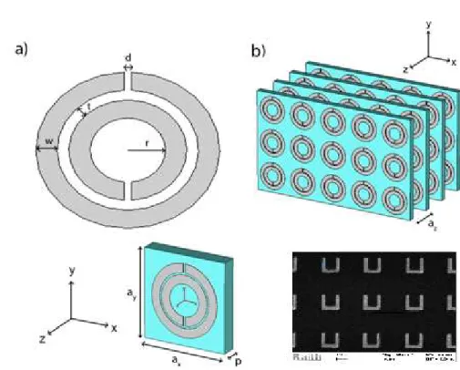
The fascinating property of SRR is the strong magnetic resonance which is due to the additional capacitive elements such as splits and gap between the rings. A typical Split Ring Resonator (SRR) structure is given in Figure 2.7.
.
Figure 2.7: Schematics of a) single SRR b) periodic arrangement of SRR array
(microwave and optical replica).
The capacitive elements (splits and gap) are utilized to achieve magnetic resonance at wavelengths much larger than the diameter of the rings.
There can be one or two rings depending on the application. The second ring is actually used for increasing the capacitance of the structure. For instance, second ring is hard to fabricate for optical applications. But it is very practical for microwave. Two rings with splits oriented oppositely. Also, there are several split ring resonator structures such as single-split ring structures and split rings with several splits [38].
Since, the periodic arrangement of the SRR (Figure 2.7.b) increases the magnetic response of SRR by strong coupling between the resonators, the unique properties such as negative permeability emerges. Also, since all parameters of SRR (a, r, d, t, w, p) are much smaller than wavelength, the response of SRR array is fit to effective medium theory. Therefore, an effective magnetic permeability (
µ
eff) and effective dielectric permittivity (ε
eff ) can be used to define the two fundamental material parameters of the structure/medium.2.3.2. Electromagnetic Resonance Mechanism of SRR
Since, split ring resonator structures are strong magnetic resonators and they respond incident electromagnetic wave by both electrical and magnetic resonance in particular bandwidths, magnetic resonance characteristics of SRRs are available for very narrow bandwidth. Also, the SRRs respond to the magnetic component of the incident wave if the incident electromagnetic wave is excited with the appropriate polarization [73, 81]. Moreover, periodically arranged SRR array is shown to exhibit negative permeability (
µ
eff <0) for frequencies close to magnetic resonance frequency (w
m) of the SRR structure [2]. Since theof SRR by coupling between the SRRs, the resonance behavior of a single SRR can also be observed by the frequency response of periodic arrangement of SRRs [73, 77]. Periodic arrangement of SRR arrays are utilized to investigate the magnetic response of SRRs; because the combined effect of periodic SRR array reveals the magnetic properties of SRR more clearly than a single SRR and negative permeability values can be obtained by strong magnetic response of SRR array.
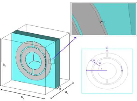
Figure 2.8: Schematic Representation of an SRR a) SRR structures modeled at Lumerical.
w: width of metal, d: gap distance, t: gap between two concentric rings, h: thickness of metal.
We used two different simulation software: 1) CST Microwave Studio for microwave which is a three dimensional full-wave solver employing the finite integration technique [177], 2) Lumerical FDTD Solutions for infrared which uses finite difference time domain method [178].
We used a previous works' [38] design parameters for estimating the parameters of SRR that will work in infrared frequency regime. For our previous work, the largest length of the SRR is 7.2 mm. Since as we scale down the size of a structure, the frequency/wavelength response for this structure scales up proportionally. This method would work for certain wavelength. Further scaling requires a different approach because of deviation of metal from perfect conductor behavior at higher frequencies
than mid-infrared. Here, we need only a rough guess. Afterwards, we will optimize our structure. In addition, since fabrication of circular nano-scale features is very hard, we used square type SRR for optical coupling which is circular-type SRRs for microwave regime and we used a single ring SRR version because alignment of concentric ring cannot be achieved very sensitive at optical regime.
As we know the resonance of 7.2 mm single ring SRR structure is at 4.1 GHz (λ ≅ 75 mm) [38], we can roughly scale to desired wavelength. In order to obtain a response at λ ≅ 1.55um, we have to start with a design
of SRR length of mm 148nm 10 * 75 10 * 55 . 1 * 2 . 7 3 6 = − −
. Also, the same scaling is
done for both the split width and width of the metallic ring:
nm mm l 148 10 * 75 10 * 55 . 1 * 2 . 7 3 6 = = −− nm mm d 4.1 10 * 75 10 * 55 . 1 * 2 . 0 3 6 = = −− nm m w 18.6 10 * 75 10 * 55 . 1 * 9 . 0 3 6 = = − −
Figure 2.9: Single ring SRR structure modeled at Lumerical. w: width of metal, d: gap
distance, h: thickness of metal.
As a rule of thumb, we take periodicity of SRR as two time the maximum length for all perpendicular directions to propagation. Since 4.1 nm and 18.6 nm is very small features for contemporary fabrication devices, we increased d, t, h and w to 50 nm which is safe for fabrication. Also we used an optically thick sapphire (
Al
2O
3). Thus, we used the followingparameters for simulation (Figure 2.9):
l=148nm (After Optimizaition: 200nm) w=50nm
d=h=50nm
Thickness of the sapphire substrate: 5um
Since the scaling down is not ideal process, we did not get a resonance at 1.55um. Then we made optimization and find the correct parameters to get resonance at approximately telecommunication frequency (1.55um- see Figure 2.10).
Phase Match Layer's (open boundary conditions) are employed along the propagation direction . Periodic boundary conditions are used for the rest of the directions. Therefore the SRR structure with its sapphire substrate is assumed to be periodic and infinite along the directions perpendicular to the propagation direction. The dip of the transmission data gives the electromagnetic resonance frequency of the structure.
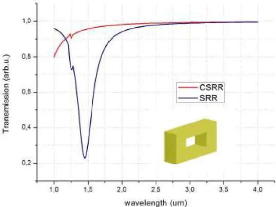
Figure 2.10: Simulation Results of SRR (l=200 nm, w=d=h 50 nm).
The resonances of SRRs not only the electromagnetic resonances but also, the periodicity of SRR may cause a band gap too. Therefore, a bandgap in the transmission spectrum of periodic SRR array medium may be due to the electromagnetic resonance or periodicity (Bragg gaps) [59]. Identification can be done by using a closed SRR (CSRR) structure in
which the splits of the SRR is closed. Since the splits of SRR play a key role in the electromagnetic resonance, closing the splits will annihilate this resonance but Bragg gaps will remain. We made numerical simulations by closing the splits of the structures in Figure 2.9. The simulation results for CSRR structure are demonstrated with results of SRR in Figure 2.11:
Figure 2.11: Simulation results of a SRR and CSRR structures. CSRR structure is depicted
in the inset CSRR (l=200 nm, w=h= 50 nm).
We observed a dip at 1.47 um in the transmission spectrum of SRR (Figure 2.11). However, no dip is observed for CSRR structure. The splits are very crucial for magnetic resonance and removing the splits of SRR prevents current to flow between the arms of splits. Therefore, the
resonance is destroyed. So, the dip is due to resonance; because, closing the splits destroys the dips at that wavelength.
Note that, the maximum length of the SRR (l = 200n m) is less than 0.1λ for the resonance at λ ≅ 1.5um. Therefore, electromagnetic resonance can be achieved by SRR structures with sub-wavelength dimensions which open up significant opportunities to design novel sub-wavelength devices. So, the major reason of the increasing amount of interest on SRR is not only the ability of achieving negative permeability but also achieving resonance with sub-wavelength dimensions. The structures that we proposed in this chapter for increasing the transmission of electromagnetic waves through sub-wavelength apertures are based on novel resonator structures and utilize the sub-wavelength resonance mechanism. We will discuss these novel structures in the following section.
2.4. Plasmonic Enhancement of Light/Wave
Plasmonics is a dominant research area for designing novel devices that utilizes the unique optical properties of metallic nanostructures to guide and deviate light/wave at subwavelength scales (nanometer scale for light). Concentrating light or create localized fields are traditionally the domain of dielectric devices. As the fundamental laws of diffraction suggests, these dielectric devices can not focus light to region less than half-wavelength, and dielectric resonators have electromagnetic volumes (
v
m) limited to 3 2 ≈λ
mv [32]. Metallic nanostructures are not limited with these limitations. Therefore, plasmonics is the leading tool for enhancement of light/wave.
The simplest structure of scientific study is probably a simple hole in a screen. However, the study and debates on the characterization of a hole in a screen have been ongoing for centuries. In the middle of the 17th
century, Grimaldi described diffraction form circular aperture, which contributed the foundation of classical optics [94, 95]. As classical optics suggests, the description of Grimaldi was valid only for a circular apertures having diameters much larger than the excitation wavelength.
Since interest in the microwave regime (longer wavelengths compared to the optical the wavelengths) increased in the 1940s as a result of World War II, the interest in the electromagnetic characterization of small (sub-wavelength) holes also increased. In 1944, Bethe gave a theoretical analysis of electromagnetic wave transmission through a sub-wavelength circular hole (aperture) in a perfectly conducting metal screen of zero thickness and suggested that the amplitude of the transmitted wave is proportional to the square of the area of sub-wavelength aperture with
( )
λ
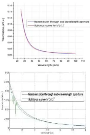
4 rk ⋅ where the radius (r) of the aperture is much smaller than the wavelength (λ) of incident electromagnetic wave (r<<λ) [25]. In other words, the transmitted wave is proportional to the square of the aperture area and is inversely proportional to the fourth power of the excitation signal’s wavelength.
According to Bethe’s ideal theoretical structure, the transmission spectra for an aperture of radius r<<λ has a rapidly decreasing transmission with the increased wavelength of incident field by the power of four. We have simulated and confirmed the Bethe’s expectation by simulating the transmission spectra of a circular hole as shown in Figure 2.12 where k is an arbitrary constant to overlap the simulation results and k ⋅
( )
rλ
4 curvefor comparison. Power of four is valid for microwave simulations in which PEC approximation is valid (Figure 2.12.a). However, the transmission spectra for an aperture of radius r<<λ has a rapidly decreasing transmission with the increased wavelength of incident field by the power of three for optical simulations as a result of non ideal metallic characteristics of metallic screen (Figure 2.12.b).
Figure 2.12: Theoretical suggestion of Bethe (λ−4 decrease) and the simulation results of transmission through a sub-wavelength aperture where r<
10
λ .
Also, an aperture in real life has a lateral dimension, which makes an aperture a waveguide-like structure and deviates the transmission result from Bethe's ideal theory. This situation is more dominant at optical regime. Because later dimension of the hole will be much more comparable to wavelength. This waveguide structure modifies the
dispersion relation of the incident field and the monotonic increase of transmission becomes distorted between a frequency band: There exists a specific frequency (wavelength) at which an incident wave in a given mode cannot be maintained (cut-off frequency/wavelength) as shown in Figure 2.13 [95].
Figure 2.13: Transmission through a sub-wavelength aperture[23].
Annular apertures that resemble coaxial waveguides are supposed to have a
TEM
0 mode without a cut-off [97, 121, 122]. However, there existsa cut-off frequency and also an extraordinary transmission peak: Several studies have shown that single sub-wavelength apertures have peaks (Figure 2.13) in their transmission spectrum as a result of the constructive excitation of propagating, surface and evanescent modes [95, 114]. In addition, the cut-off frequency cannot be sharply defined while considering metals at optical regime (with finite conductivity); because the transmission regime goes continuously from the propagative to evanescent regime as the wavelength increases [95].
When the finite conductivity of the metal is taken into account, the cut-off wavelength of the aperture is larger compared to an aperture in a perfectly conducting plane [102]. Also, transmission through a sub-wavelength aperture further decreases due to the non-zero depth of the aperture [103, 104]. All of these studies reveal that Bethe’s theory holds for idealized situations, in which the enhancement of electromagnetic wave propagation beyond the limit of Bethe’s suggestion could be obtained by utilizing novel methods to improve the coupling of incident wave and aperture [98-101].
Advances in the characterization and fabrication techniques enable researchers to reduce severe effects of extremely high transmission losses and diffraction of electromagnetic waves through sub-wavelength aperture transmission. In 1998, “extraordinary optical transmission (EOT) through a sub-wavelength hole array in a metal screen” phenomena was reported by the seminal work of Ebbesen et al. [24]. It has been shown that the coupling of light with the Surface Plasmons (SP) of a two dimensional array of sub-wavelength holes in turn causes a strong enhancement of transmitted light, which is above the limit of Bethe’s prediction. This new era has attracted the interest of researchers on the enhancement of “light/electromagnetic wave” transmission through sub-wavelength apertures. Various studies on the characterization of EOT phenomenon approved the involvement of Surface Plasmons; and also showed that the interplay between light and the resonant excitation of SPs, which are induced by a periodic array of holes, causes the EOT [106-109].
![Figure 2.4: µ eff -w diagram for ideal single SRR structure [15].](https://thumb-eu.123doks.com/thumbv2/9libnet/5913213.122574/37.892.290.680.739.1075/figure-µ-eff-diagram-ideal-single-srr-structure.webp)
![Figure 2.5: Negative refraction of electromagnetic wave through a left-handed medium[38]](https://thumb-eu.123doks.com/thumbv2/9libnet/5913213.122574/40.892.343.616.349.598/figure-negative-refraction-electromagnetic-wave-left-handed-medium.webp)
![Figure 2.13: Transmission through a sub-wavelength aperture[23].](https://thumb-eu.123doks.com/thumbv2/9libnet/5913213.122574/54.892.267.681.346.647/figure-transmission-sub-wavelength-aperture.webp)