ORIGINAL ARTICLE
Influence of diamond tool chamfer angle on surface integrity
in ultra-precision turning of singe crystal silicon
Yigit Karpat1,2,3
Received: 11 June 2018 / Accepted: 18 November 2018 / Published online: 22 November 2018 # Springer-Verlag London Ltd., part of Springer Nature 2018
Abstract
Ultra precision diamond machining enables the economical production of freeform optics on infrared materials such as silicon. To produce optics with acceptable surface integrity, it is important to have a good understanding of process-work material interaction between diamond tool and brittle and hard single crystal IR materials. Chamfered cutting edges are known to have high strength, which makes them suitable for machining difficult-to-cut materials. This study investigates the influence of chamfer angle on the surface integrity of silicon. Diamond tool chamfer angles of− 20°, − 30°, and − 45° are considered under practical diamond turning conditions of single crystal silicon. State-of-the-art techniques were used to investigate the surface integrity of the machined silicon surfaces. The results show that chamfer angle of 30° yields more favorable results compared to 20° and 45° under the conditions tested. The results indicate the complex interplay between tool geometry and process parameters in reaching an acceptable level of surface integrity. A machinability map indicating ductile and brittle machining conditions for 30° cham-fered diamond tool has been presented which includes directly transferable knowledge to the precision machining industry. Keywords Diamond machining . Surface integrity . Silicon . Phase transformation
1 Introduction
Freeform optics offers a multitude of improvements over tra-ditional spherical form optical systems [1]. A novel example would be compound eye systems, where the micro lenses are machined on curved substrate, mimicking the structure of a fly’s eye as observed in nature. An active research subject is to obtain freeform optics on infrared (IR) materials and as a result extend the advantages of freeform optics beyond visible light applications [2–4]. Ultra precision diamond machining enables economical production of freeform optics made from IR materials. A good understanding of process-work material interaction between diamond cutting tool and brittle and hard
single crystal IR materials such as silicon and germanium is important to the economical production of freeform optics with acceptable surface integrity.
Tool-work material engagement conditions change contin-uously due to the complex surface geometry of the freeform surfaces. Using slow slide servo technique to machine freeform optics requires the fragile diamond tool tip to work under interrupted machining conditions, which may lead to edge chipping [5]. Machining with chipped or worn diamond tools results in cracks on the machined surface, which hinders the surface integrity of the machined surface and adversely affects optical performance. Diamond cutting tools with chamfered edge preparations have the advantage of protecting the cutting edge from chipping [6]. Chamfered diamond tools have zero rake angle, but their cutting edges are chamfered at a specified angle and width. This study considers the influence of chamfer angle on the surface integrity of single crystal silicon material.
When IR materials are machined, machining strategy and parameters must be set carefully in order to reach high surface quality without sacrificing productivity. A good understand-ing of the deformation mechanism of sunderstand-ingle crystal IR mate-rials has been a research subject for a long time [7]. High pressure at the tip of the fragile diamond tool is necessary so
* Yigit Karpat
1
Department of Industrial Engineering, Bilkent University, Ankara, Turkey
2 Department of Mechanical Engineering, Bilkent University,
Ankara, Turkey
3
UNAM-National Nanotechnology Research Center and Institute of Materials Science and Nanotechnology, Bilkent University, Ankara, Turkey
that the material goes through a phase transformation process and behaves like a metal, producing ductile chips, and thereby producing crack-free surfaces. It is known as ductile mode machining [8,9]. The critical chip thickness, beyond which cracks reach the machined surface and cannot be cleaned in successive machining passes, has been observed to increase with increasing negative rake angle [10,11]. Increasing rake angle increases the thrust forces. When the high pressure is released, an amorphous layer of silicon forms on the surface during material recovery, and its thickness is directly related to the machining conditions (feed and depth of cut) and diamond tool geometry and rake angle [12]. Large negative (20°–50°) rake angle diamond tools are usually used in diamond machin-ing of smachin-ingle crystal silicon with the aim of increasmachin-ing hydro-static pressures at the cutting zone. Rake angles larger than 50° result in debris accumulation problem in front of the cut-ting edge. In addition to rake angle, cutcut-ting edge radius, nose radius, and waviness of the nose radius of the diamond tool are other factors known to affect surface roughness significantly. Diamond machining parameters and tool geometry affect the tool-work material contact conditions and significantly influ-ence the subsurface integrity of the machined surface. Yan et al. [12] investigated the subsurface damage in silicon using laser micro Raman spectroscopy and cross-sectional transmis-sion electron microscopy (TEM). They concluded that thick-ness of the machining-induced amorphous layer strongly de-pends on the rake angle and depth of cut. Yan et al. [13] per-formed nano scale plunge cutting experiments on silicon using different tool rake angles at different crystal directions. They observed that critical depth of cut increased with increasing rake angle to negative 45°. It must be noted that plunge cutting experiments were performed at low cutting speed. Cutting speed affects the thermal aspects of the machining process. Wang et al. [14] studied the influence of anisotropy of ma-chined surfaces during diamond turning of silicon and observed that tools with− 40° rake angle yielded better results that − 25° rake angle tools. They related the improvement to increasing number of dislocations during plastic deformation. Patten and Gao [15] increase the rake angle from− 45° to − 85° and ob-served the increase in thrust forces and cutting angles. Durazo-Cardenas et al. [16] studied the diamond tool wear and ob-served that− 25° rake angle yielded better performance com-pared to− 40° rake angle. They also indicated the influence of specific diamond gem quality used in the experiments. Fang and Venkatesh [17] used a 0° rake angle tool but selected the uncut chip thickness to be less than tool edge radius. Therefore, the effective rake angle was also negative. They obtained better surface finish compared to− 25° rake angle tool. Mir et al. [18] recently investigated the influence of rake angle on diamond turning of silicon. No direct correlation between tool perfor-mance and rake angle was observed. They found that diamond tool with a negative 30° rake angle performed poorly during experiments compared to negative 25° and 40°.
It is a challenge to find optimized process conditions for the machining of silicon that will yield high surface quality and low subsurface damage. The nose radii of chamfered diamond tools have a circular profile whereas the large negative rake angle diamond tools have an elliptical form which is due to diamond tool grinding process. As a result, the rake angle along the nose radius remains constant in chamfered tools. In addition, due to zero rake angle on the top face of the tool, application of cutting fluid is easier which helps evacuating silicon debris away from cutting zone. Therefore, investigat-ing the influence of chamfer angle may help understandinvestigat-ing the relationship between process parameters and surface integrity. This study uses single point diamond turning tests with cham-fered diamond tools together with areal surface characteriza-tion and subsurface damage deteccharacteriza-tion techniques to investi-gate the influence of chamfer angle and process conditions on the surface integrity of single crystal silicon.
2 Experimental setup
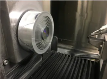
An ultra-precision diamond turning machine Moore Nanotechnology 350 FG was used in the experiments. Figure1shows the experimental setup where a polished sili-con work material having (100) crystal plane and 50 mm di-ameter with 3 mm thickness was placed on a vacuum chuck. Nanoindentation tests were conducted to measure the hard-ness (1286 HV) and elasticity modulus (168 GPa) of the sam-ple. Machining experiments were conducted under heavy use of coolant (odorless mineral spirit). Machined surfaces were analyzed using confocal laser microscope Keyence VKX110 (with 100× objective lens), white-light interferometer (NewView-7200, Zygo Corporation), and a laser micro-Raman spectrometer (WITec alpha series, laser wavelength of 532 nm, and 50× objective lens with NA 0.75 resulting around ~ 865 nm laser spot size).
Chamfered single crystal diamond tools were used in this study. Chamfered tools have the ability to keep neg-ative rake angle constant along the nose radius of the tool and thereby maintaining uniform chip formation. They also tend to accumulate fewer chips on the rake face during machining since only the cutting edge has negative rake angle. Design parameters of chamfered di-amond tools are chamfer angle and width. In this study, chamfered tools having 20°, 30°, and 45° chamfer angle with ~ 2–3 μm chamfer width were used (ALMT, Japan). Nose radius of the tools was 0.53 mm. Waviness along the cutting edge is less than 0.5 μm, clearance angle of 10°. Figure 2a shows the tip image of diamond tools where the chamfer land can be seen. Figure 2b shows the machining parameters as feed (f ) and depth of cut (ap). Uncut chip thickness varies with angle θ along the
nose radius (R). If the maximum value of uncut chip thickness (tu) is less than the chamfer width (L), only
the chamfered region of the tool performs the cutting operation.
3 Influence of chamfer angle on surface
topography and integrity
In the experiments, polished silicon lenses were machined at different depth of cut and feed conditions as shown in Table1. The aim is to mimic varying contact conditions typical during machining of freeform surfaces and eliminate the influence of machining-induced subsurface damage at each machining pass. Spindle speed was kept constant at 2000 rpm. Different polished silicon samples were used for each chamfer angle in experiments.
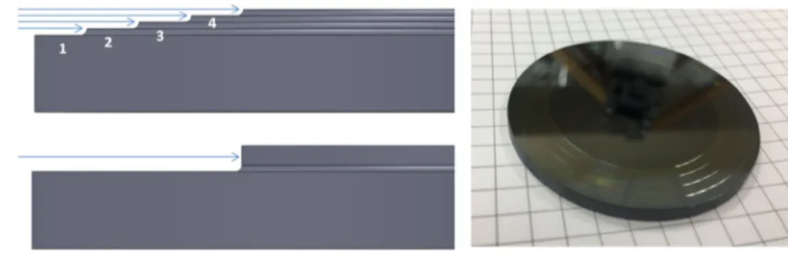
Figure3explains the first and second phases of the exper-iments. Regions of 2 mm length were machined. In the first phase (phase I in Table1), depth of cut decreased from 10 to 4 μm at varying feeds. In the second phase of the tests, a constant feed rate and spindle speed (2 μm/rev and 2000 rpm) were used to machine the stepped surface from previous tests which allows for investigating the influence of increasing depth of cut (4–6–8–10–12 μm) on the surface roughness and subsurface damage. In the third phase, depth of cut was kept at 2μm and feed was increased from 1 to 3μm/rev on the remaining part of the polished surface. The last phase was only performed with 30° chamfered tools due to limited availability of the tools. Machining conditions were selected based on practical silicon cutting parameters.
Surface topographies of silicon samples were investigated using both confocal laser topography and scanning white light interferometer. Measurement data were processed on Mountains Map software 7.4 based on ISO 25178 standard [19]. First, surement outliers were filtered out. Then, leveling of the mea-sured data was performed using least square plane method. A spatial smoothing filter (filter size 3 × 3) was then applied. Finally, a Gaussian filter with 8-μm cut-off was applied to
Fig. 2 a Chamfered diamond tool edge profile and b tool and process parameters
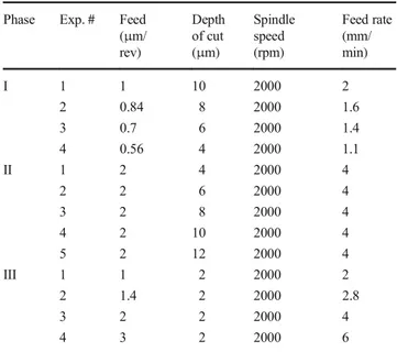
Table 1 Experimental conditions Phase Exp. # Feed
(μm/ rev) Depth of cut (μm) Spindle speed (rpm) Feed rate (mm/ min) I 1 1 10 2000 2 2 0.84 8 2000 1.6 3 0.7 6 2000 1.4 4 0.56 4 2000 1.1 II 1 2 4 2000 4 2 2 6 2000 4 3 2 8 2000 4 4 2 10 2000 4 5 2 12 2000 4 III 1 1 2 2000 2 2 1.4 2 2000 2.8 3 2 2 2000 4 4 3 2 2000 6
separate roughness (S-L) and waviness (S-F) surfaces. Measurement sample size was 144μm × 108 μm. Figure 4 shows the surface micrographs for 20° and 30° tools under the first phase and third (I-3) experimental conditions where no pitting damage was observed on the surface.
Figure5shows areal surface roughness (Sa) and maximum height of the surface (Sz) values for each machining case in
phase I. Based on the results, in terms of Sa, 30° chamfered tool yielded overall better results compared to 20° and 45° diamond tools. A similar trend was observed for root mean square height roughness, Sq where the values were around 25% more than Sa. The best result obtained at second exper-imental case for all tools. In experiments #3 and 4, as depth of cut and feed decreased further, the surface roughness values did not improve compared to experiments #1 and 2. According to maximum height of the surface (Sz) measure-ments, 20° and 30° tools yielded better results than 45° cham-fered diamond tool. It must be noted that at low uncut chip thickness values, due to the cutting edge radius of the tool (around 50 nm), the effective rake angle increases, which hin-ders the surface generation. In addition, size effect issues are likely to initiate at such conditions.
In the second phase of the experiments, the silicon samples were machined at constant feed (2 μm/rev) and varying depth of cut (4–6–8–10–12 μm) conditions as explained in Fig. 3. During these experiments, ductile, ductile-to-brittle transition, and brittle machining modes were observed, depending on the crystal direction and machining parameters as shown in Fig.6.
At low depth of cuts (2 and 4μm), machining was per-formed in ductile mode. Surface roughness started to deterio-rate at 6μm and transitioned into brittle mode at depth of cut above 8μm. The resulting surface yields a typical four-fold symmetry pitting damage arms which is typical for silicon
Fig. 3 Experiment strategy (phase I top, phase II bottom) and machined silicon sample
Fig. 4 Surface micrograph fora 20°, b 30° chamfered tool in experiment #I-3
Fig. 5 Areal surface roughness and maximum height of the surface as function of different experiments
with (100) crystal plane orientation as shown in Fig.6. Critical depth of cut can be identified to be between 6 and 8μm for
feed of 2μm/rev (4 mm/min) for all tools where machining transitioned from ductile to brittle mode.
Laser micro Raman tests were performed for all machining experiments in phases I and II. Figure7shows the Raman spec-trum of machined surfaces corresponding to Exp #I-3 and I-4 for
Fig. 6 Machined sample surface after second phase of the experiments (experimental conditions 1–5 are shown on the figure)
Fig. 7 Raman spectrum of the machined surfaces under experimental conditionsa experiment #I-3 andb experiment #I-4
all tools. In Fig.7a, for Exp #I-3, there is a sharp peak at 521 cm−1and no significant peak at other Raman shifts for all tools. It indicates that the structural changes are small and the Raman measurement system used here could not detect any changes. However, peak intensity values are different, with the
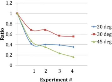
highest at 30° and lowest at 45°. In Fig.7b, while similar mea-surements were obtained for 20° and 30°, a small peak at 470 cm−1for 45° indicates that a thin layer of silicon was trans-formed into amorphous state (a-Si). It must be noted that feed and depth is lower in Exp#I-3 than Exp #I-4. There seems to be a correlation between Raman measurements and Sz measurements on the surface. Yan et al. [20] proposed a method to estimate the thickness of the amorphous layer by using Raman intensity ratio information. A similar approach has been adopted in this study. Figure8 shows the intensity ratio for each tool at four experi-mental conditions in finish machining tests. Intensity level ob-tained at the polished surface of the silicon material was consid-ered as the reference value, and peak intensity values measured from the machined surfaces were considered to calculate a rela-tive intensity ratio for each case. According to results, the 30° chamfered diamond tool has a higher ratio for all experimental cases, indicating a smaller effect on the surface structure. With decreasing feed and depth of cut from finishing experiments #I-1 to #I-4, as Sz tends to increase (shown in Fig.5), the intensity ratio also decreases. For 45° tool, Sz value around 25–30 nm may be the limit for amorphous phase formation based on Figs.5 and7.
Figure 9 shows the Raman measurements for second phase of experiments that machined large depth of cuts. As depth of cut increased from 4 to 6 μm, amorphous layer formation on the surface increases significantly as evidenced from the peak at 470 cm−1. When the depth of cut further increased from 6 to 8μm, intensity of the peak at 521 cm−1 corresponding to Si-I significantly decreases and machined surface mostly transforms into amorphous phase. Phase transformation is due to the high pressures applied by the tip of the diamond tool on the silicon sur-face. It is important to maintain pressure during machin-ing more than 10 GPa to obtain ductile chip formation [12]. On the other hand, exceedingly high pressures result in micro cracks on the surface. Increasing depth of cut usually leads to lower machining pressure since the con-tact area between the tool and the work material increases
Fig. 9 Influence of increasing depth of cut on Raman shift with 30° tool
(a)
(b)
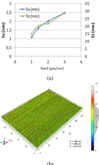
0 5 10 15 20 25 30 35 0 0,5 1 1,5 2 2,5 3 0 1 2 3 4 Sz (n m ) ) m n( aS Sa (nm) Sz (nm) Feed (μm/rev)Fig. 10 a Influence of feed on Sa and Sz for 30° chamfer angle and b surface topography for 3μm/rev and 2 μm depth of cut
and average machining forces decrease due to brittle frac-tures occurring during machining.
4 Influence of feed on surface topography
and integrity
Additional tests (third phase in Table 1) were conducted to validate the results obtained with 30° chamfered tool on the top surface of the silicon to observe the influence of increasing feed on surface roughness. Depth of cut was kept constant at 2μm, spindle speed as kept at 2000 rpm, and feed increased from 1 to 1.4, 2, and 3 μm/rev. Figure10a shows the influence of feed on surface topog-raphy. Figure 10b shows the S-L surface topography at feed of 3μm/rev. Areal surface roughness (Sa) and max-imum height of the surface (Sz) increase with increasing feed, as expected. The areal surface roughness Sa = 1 nm obtained at 1μm/rev is in close agreement with the pre-vious tests in the literature [11] indicating the equivalent performance of chamfered tools.
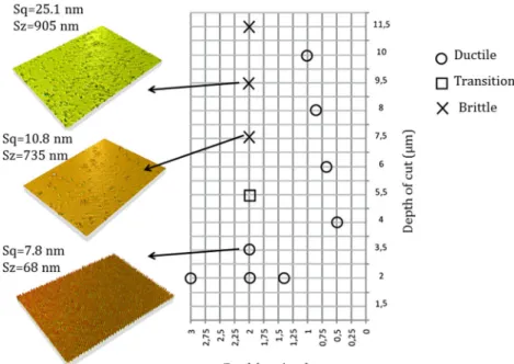
Figure11shows the summary of experimental studies for chamfered diamond tools. In this figure, the influence of depth of cut and feed on machining characteristics can be seen. The interplay between feed and depth of cut can be seen as increasing feed requires depth of cut to be decreased. At low feed, depth of cut can be increased up to 10μm in ductile model cutting.
5 Conclusions
In this study, ultra-precision machining of single crystal silicon was performed with chamfered diamond tools.
Influence of chamfer angle and process parameters (feed and depth of cut) on areal surface roughness and sub-surface damage has been investigated using an experi-mental approach. Based on the results obtained at ex-perimental conditions considered in this study, under finish machining conditions, diamond tool with 30° chamfer angle performed better than 45° chamfer angle diamond tool. In terms of areal surface roughness values, performance of 30° chamfer angle diamond tool was observed to be slightly better than 20° chamfer diamond tool. Using 30° chamfer angle tool at finish machining conditions of 2 μm depth of cut and 1 μm/ rev feed yielded areal surface roughness values around 1 nm, which satisfies the high standards in the optics industry. Low subsurface damage was detected at finish machining conditions with the measurement device used in this study. Based on higher feed and depth of cut experiments with diamond tool having 30° chamfer an-gle, pitting damages on the machined surface appear around 7–8 μm depth of cut value resulting in low surface integrity. Raman analysis of the machined sur-faces indicated the phase transformation of silicon into an amorphous phase.
Acknowledgments The author would like to thank the Ministry of Development of Turkey (HAMIT-Micro System Design and Manufacturing Research Centre).
Funding information This work was financially supported by the Turkish Scientific and Technological Research Council of Turkey (TUBITAK) through project 115M699.
Publisher’s Note Springer Nature remains neutral with regard to jurisdic-tional claims in published maps and institujurisdic-tional affiliations.
Fig. 11 Summary of machining characteristics with 30° chamfered diamond tool
References
1. Fang FZ, Zhang XD, Weckenmann A, Zhang GX, Evans C (2013) Manufacturing and measurement of freeform optics. CIRP Ann Manuf Technol 62:823–846
2. Fang FZ, Zhang XD, Gao W, Guo YB, Byrne G, Hansen HN (2017) Nanomanufacturing—perspective and applications. CIRP Ann Manuf Technol 66:683–705
3. Owen J, Davies M, Schmidt D, Urruti E (2015) On the ultra-precision diamond machining of chalcogenide glass. CIRP Ann Manuf Technol 64:113–116
4. Owen JD, Troutman JR, Harriman TA, Zare A, Wang YQ, Lucca DA, Davies MA (2016) The mechanics of milling of germanium for IR applications. CIRP Ann Manuf Technol 65:109–112 5. Mukaida M, Yan J (2017) Ductile machining of single-crystal
sili-con for microlens arrays by ultraprecision diamond turning using a slow tool servo. Int J Mach Tools Manuf 115:2–14
6. Tang X, Nakamoto K, Obata K, Takeuchi Y (2013) Ultraprecision micromachining of hard material with tool wear suppression by using diamond tool with special chamfer. CIRP Ann 62:51–54 7. Goel S, Luo X, Agrawal A, Reuben RL (2015) Diamond machining
of silicon: a review of advances in molecular dynamics simulation. Int J Mach Tools Manuf 88:131–164
8. Blake PN, Scattergood RO (1990) Ductile-regime machining of germ5anium and silicon. J Am Ceram Soc 73(4):949–957 9. Lucca DA, Chou P, Hocken RJ (1998) Effect of tool edge geometry
on the nanometric cutting of Ge. CIRP Ann Manuf Technol 47(1): 475–478
10. Shibata T, Fujii S, Makino E, Ikeda M (1996) Ductile-regime turn-ing mechanism of sturn-ingle crystal silicon. Precis Eng 18:129–137
11. Leung TP, Lee WB, Lu XM (1998) Diamond turning of silicon sub-strates in ductile-regime. J Mater Process Technol 73(1–3):42–48 12. Yan J, Asami T, Harada H, Kuriyagawa T (2009) Fundamental
investigation of subsurface damage in single crystalline silicon caused by diamond machining. Precis Eng 33:378–386
13. Yan J, Asami T, Harada H, Kuriyagawa T (2012) Crystallographic effect on subsurface damage formation in silicon microcutting. CIRP Ann Manuf Technol 61:131–134
14. Wang M, Wang W, Lu Z (2012) Anisotropy of machined surfaces involved in the ultra-precision turning of single-crystal silicon—a simulation and experimental study. Int J Adv Manuf Technol 60(5): 473–485
15. Patten JA, Gao W (2001) Extreme negative rake angle technique for single point diamond nano-cutting of silicon. Precis Eng 25(2): 165–167
16. Durazo-Cardenas I, Shore P, Luo X, Jacklin T, Impey SA, Cox A (2007) 3D characterisation of tool wear whilst diamond turning silicon. Wear 262(3–4):340–349
17. Fang FZ, Venkatesh VC (1998) Diamond cutting of silicon with Nanometric finish. CIRP Ann Manuf Technol 47(1):45–49 18. Mir A, Luo X, Cheng K, Cox A (2017) Investigation of influence of
tool rake angle in single point diamond turning of silicon. Int J Adv Manuf Technol 94:2343–2355. https://doi.org/10.1007/s00170-017-1021-7
19. Characterisation of Areal Surface Texture Richard Leach Editor Springer, ISBN 978-3-642-36458-7
20. Yan J, Asami T, Kuriyagawa T (2008) Nondestructive measure-ment of machining-induced amorphous layers in single-crystal sil-icon by laser micro-Raman spectroscopy. Precis Eng 32:186–195