HIGH PERFORMANCE FLOATING GATE
MEMORIES USING GRAPHENE AS
CHARGE STORAGE MEDIUM AND
ATOMIC LAYER DEPOSITED
HIGH-K DIELECTRIC LAYERS AS
TUNNEL BARRIER
A THESIS
SUBMITTED TO THE MATERIALS SCIENCE AND NANOTECHNOLOGY PROGRAM
OF THE GRADUATE SCHOOL OF ENGINEERING AND SCIENCE OF BILKENT UNIVERSITY
IN PARTIAL FULFILLMENT OF THE REQUIREMENTS FOR THE DEGREE OF
MASTER OF SCIENCE
By
Deniz Kocaay
January, 2013
I certify that I have read this thesis and that in my opinion it is fully adequate, in scope and in quality, as a thesis for the degree of Master of Science.
Assist. Prof. Dr. Aykutlu Dana (Supervisor)
I certify that I have read this thesis and that in my opinion it is fully adequate, in scope and in quality, as a thesis for the degree of Master of Science.
Assist. Prof. Dr. Coşkun Kocabaş
I certify that I have read this thesis and that in my opinion it is fully adequate, in scope and in quality, as a thesis for the degree of Master of Science.
Assist. Prof. Dr. Necmi Bıyıklı
Approved for the Graduate School of Engineering and Science:
Prof. Dr. Levent Onural Director of Graduate School
ABSTRACT
HIGH PERFORMANCE FLOATING GATE MEMORIES
USING GRAPHENE AS CHARGE STORAGE MEDIUM
AND ATOMIC LAYER DEPOSITED HIGH-K
DIELECTRIC LAYERS AS TUNNEL BARRIER
Deniz Kocaay
M.S. in Materials Science and Nanotechnology Supervisor: Assist. Prof. Dr. Aykutlu Dana
January, 2013
With the ongoing development in portable electronic devices, low power consumption, improved data retention rate and higher operation speed are the merits demanded by modern non-volatile memory technology. Flash memory devices with discrete charge-trapping media are regarded as an alternative solution to conventional floating gate technology. Flash memories utilizing Si-nitride as charge storage media dominate due to enhanced endurance, better scaling capability and simple fabrication. The use of high-k dielectrics as tunnel layer and control layer is also crucial in charge-trap flash memory devices since they allow further scaling and enhanced charge injection without data retention degradation. Atomic layer deposition (ALD) is a powerful technique for the growth of pinhole-free high-k dielectrics with precisely controlled thickness and high conformality. The application of graphene as charge trapping medium in flash memory devices is promising to obtain improved charge storage capability with miniaturization. Graphene acts as an effective charge storage medium due to high density of states in deep energy levels.
In this thesis, we fabricate graphene flash memory devices with ALD-grown HfO2/AlN as tunnel layer and Al2O3 as control layer. Graphene oxide nanosheets
The graphene layer is obtained by spin-coating of water soluble graphene oxide suspension followed by a thermal annealing process. Memory performance including hysteresis window, data retention rate and program transient characteristics for both electron and hole storage mechanisms are determined by performing high frequency capacitance-voltage measurements. For comparing the memory effect of graphene on device performance, we also fabricate and characterize identical flash capacitors with Si-rich SiN layer as charge storage medium and HfO2 as tunnel oxide layer. The Si-nitride films are deposited with
high SiH4/NH3 gas flow ratio by plasma-enhanced chemical vapor deposition
system.
Graphene flash memory devices exhibit superior memory performance. Compared with Si-nitride based cells, hysteresis window, retention performance and programming speed are both significantly enhanced with the use of graphene. For electron storage, graphene flash memory provides a saturated flat band shift of 1.2 V at a write-pulse duration of 100 ns with a voltage bias of 5 V. The high density of states and high work function of graphene improve the memory performance, leading to increased charge storage capability, enhanced retention rate and faster programming operation at low voltages.
The use of graphene as charge storage medium and ALD-grown high-k dielectrics as tunnel and control layers improves the existing flash technology and satisfies the requirements including scalability, at least 10-year retention, low voltage operation, faster write performance and CMOS-compatible fabrication.
ÖZET
YÜK DEPOLAMA ORTAMI OLARAK GRAFEN,
TÜNELLEME BARİYERİ OLARAK ATOMİK KATMAN
KAPLAMA TEKNİĞİYLE ÜRETİLMİŞ YÜKSEK-K
DİELEKTRİK KULLANILARAK OLUŞTURULAN
YÜKSEK PERFORMANSLI İKİNCİL KAPILI HAFIZA
YAPILARI
Deniz Kocaay
Malzeme Bilimi ve Nanoteknoloji, Yüksek Lisans Tez Yöneticisi: Yar. Doç. Dr. Aykutlu Dana
Ocak, 2013
Taşınabilir elektronik cihaz teknolojisinde süregelen gelişim ile birlikte düşük güç tüketimi, gelişmiş veri tutma oranı ve daha yüksek çalışma hızı, modern flaş bellek teknolojisi tarafından talep edilen özellikler haline gelmiştir. Ayrık yük yakalama ortamı taşıyan flaş bellek aygıtları, geleneksel ikincil kapılı hafıza teknolojisine alternatif bir çözüm olarak kabul edilmektedir. Yük depolama ortamı olarak Si-nitrür kullanarak geliştirilmiş flaş bellekler dayanıklılık, daha iyi ölçekleme yeteneği ve basit üretimi nedeniyle yaygın olarak kullanılmaktadır. Tünelleme ve kontrol bariyerleri olarak Atomik katman kaplama (ALD) tekniğiyle üretilmiş yüksek-k dielektrikli filmlerin kullanımı, daha küçük yapıların üretimine ve verinin tutulma zamanını etkilemeksizin daha fazla yük tutulumuna elverdiğinden flaş bellek yapıları için çok önemlidir. ALD tekniği tam olarak kontrol kalınlığı ve yüksek konformalite sağlayabildiğinden deliksiz yüksek-k dielektrikli film büyütülmesi için çok güçlü bir tekniktir. Flaş bellek aygıtları için yük yakalama aracı olarak grafen kullanılması, geliştirilmiş yük depolama kapasitesine sahip daha küçük ölçekli aygıtlar elde etmek açısından umut vericidir. Grafen, derin enerji seviyelerinde daha fazla yük tutulabilecek yer bulunması nedeniyle etkili bir yük depolama ortamı olarak görülmektedir.
Bu tez çalışmasında, ALD ile büyütülmüş tünel katmanı olarak HfO2/AlN
ve kontrol katmanı olarak Al2O3 malzemeler içeren grafen flaş bellek cihazları
imal edilir. Grafen oksit nanotabakalar Hummers yöntemi ile doğal grafitin asit eksfoliyasyonu ile elde edilmektedir. Grafen tabakası suda çözünür grafen oksit süspansiyonunun döndürerek kaplanması ve ısıl tavlama işlemi ile elde edilir. Histerezis penceresi, veri saklama oranı ve elektron/deşik depolama mekanizmalarını içeren bellek performansı yüksek frekansta kapasitans-voltaj ölçümleri yapılarak belirlenir. Grafenin cihaz performansına etkisini karşılaştırmak için, yük saklama ortamı olarak Si-zengin SiN tabaka kullanan özdeş flaş kapasitörler imal edilmiş ve karakterizasyonu yapılmıştır. Si-nitrür filmler yüksek SiH4/NH3 gaz akış oranı ile plazma destekli kimyasal buhar
biriktirme sisteminde kaplanmıştır.
Grafen flaş bellek cihazları üstün bellek performansı gösterir. Si-nitrür temelli hücrelerle ile karşılaştırıldığında, histerezis pencere, veri tutma performansı ve programlama hızı grafen kullanımı ile önemli ölçüde geliştirilmiştir. Elektron depolama için grafen flaş bellek 5 V gerilimde ve 100 ns darbe süresi ile 1.2 V düz bant kayması sağlar.
Grafenin yük depolama ortamı ve ALD ile büyütülen yüksek-k dielektriklerin tünel ve kontrol katmanları olarak kullanılması mevcut flaş teknolojisini geliştirir ve en az 10 yıllık saklama, düşük voltajda çalışma, hızlı yazma performansı ve CMOS-uyumlu fabrikasyon gibi gereksinimleri karşılar.
Acknowledgements
I would like to express my sincere gratitude, first and foremost, to my supervisor, Assist. Prof. Dr. Aykutlu Dana for his outstanding support, encouragement and guidance throughout my research. I have learned a lot of valuable knowledge and the way of thinking as a scientist but also as a person. I would like to thank the committee members, Assist. Prof. Dr. Coşkun Kocabaş and Assist. Prof. Dr. Necmi Bıyıklı for their generous guidance and review on this work.
I also would like to expand my thanks to my group members: Mustafa Ürel, Okan Öner Ekiz, Sencer Ayas, Hasan Güner, Serkan Karayalçın, Andi Çupallari and Ayşegül Abdelal. I also would like to thank UNAM engineers Fatih Büker, Semih Yaşar, Adem Saraç, Fikret Piri and Mustafa Kemal Ruhi.
I would like to thank my clean room family: Feyza Bozkurt-Oruç, İnci Dönmez, Çağla Özgit-Akgün, Engin Çağatay, Mehmet Alican Noyan, Fatih Bilge Atar, Levent Erdal Aygün and Oğuz Hanoğlu. It was a great experience that I worked and enjoyed my time in the clean room with all of you. I would like to thank my dear friends: Gözde Turan, Zeynep Seval, Hülya Budunoğlu, Gülesin Eren, Aylin Civan and Pınar Beyazkılıç.
My deepest gratitude goes to my parents Fundagül and Çetinkaya Kocaay for their encouragement, support, patience and endless love. Special thanks go to my dear brother Aziz Berkin Kocaay for his help for figures in the thesis.
Contents
1 Introduction ... 1
2 Device Physics ... 4
2.1 Overview of Non-Volatile Memory ... 4
2.2 Performance Considerations of Flash Memories ... 5
2.3 Floating Gate Flash Memories ... 7
2.4 Charge-Trapping Flash Memories ... 9
2.5 MOS Physics ... 10 2.5.1 Accumulation ... 11 2.5.2 Depletion ... 11 2.5.3 Inversion ... 12 2.6 Tunneling Mechanism ... 13 2.6.1 Direct Tunneling ... 14 2.6.2 Fowler-Nordheim Tunneling ... 15 2.6.3 Trap-assisted Tunneling ... 15
3 Possible Solutions to the Scaling Issue ... 16
3.1 Nanocrystal Flash Memory ... 16
3.1.1 Semiconductor Nanocrystal Preparation Methods ... 17
3.1.2 Metal Nanocrystals ... 18
3.1.3 Basic Principle of Operation ... 20
3.1.4 Challenges of Nanocrystal Memories ... 22
3.2 High-k Dielectrics ... 23
3.2.1 Reliability Issues of High-k Dielectrics ... 28
3.3 Graphene ... 29
3.3.1 Graphene Growth Techniques ... 30
3.3.1.2 Epitaxial Growth ... 33
3.3.1.3 Chemical Techniques ... 34
3.3.2 Graphene in Flash Memory Applications... 35
3.4 ALD Basics ... 36
4 Device Fabrication and Characterization Methods ... 39
4.1 Device Fabrication ... 39
4.1.1 Wafer Cleaning ... 40
4.1.2 Back Contact Deposition ... 41
4.1.3 Active Region Definition ... 43
4.1.4 Gate Stack Formation ... 44
4.1.5 Gate Contact Definition ... 46
4.2 Characterization Methods ... 46
4.2.1 Spectroscopic Ellipsometry ... 46
4.2.2 Atomic Force Microscopy ... 47
4.2.3 Semiconductor Parameter Analyzer ... 48
5 Results and Discussion ... 49
5.1 Characterization of Graphene ... 49
5.1.1 SEM ... 49
5.1.2 AFM ... 50
5.1.3 Raman ... 51
5.2 Electrical Characterization of Control Samples ... 52
5.3 Surface Functionalization of Graphene ... 54
5.4 Electrical Characterization of p-type Graphene Flash Memories ... 55
5.5 Electrical Characterization of n-type Graphene Flash Memories ... 59
5.6 Electrical Characterization of p-type SiN Flash Memories ... 62
5.8 Comparison of Graphene and SiN as Charge Storage Medium for Electron
Storage ... 68
5.9 Comparison of Graphene and SiN as Charge Storage Medium for Hole Storage ... 72
5.10 Graphene Flash Memory with AlN as Tunnel Layer ... 76
5.10.1 Device Fabrication ... 76
5.10.2 Electrical Characterization of AlN Thin Film ... 77
5.10.3 Electrical Characterization of the Memory Structure ... 78
6 Conclusions ... 84
List of Figures
Figure 2.1: Device Structure of Conventional FG Flash Cell ... 7
Figure 2.2: Device Structures of SONOS and Nanocrystal Flash Cells ... 10
Figure 2.3: Energy band diagrams and corresponding block charge diagrams in an ideal n-type MOS capacitor. ... 13
Figure 2.4: Tunneling Mechanisms ... 14
Figure 3.1: Energy Band Diagram of a Flash Cell with Metal Nanocrystals ... 19
Figure 3.2: Band gaps and band offsets of various high-k materials [37]. ... 25
Figure 3.3: Inverse relation between band gap and dielectric constant of various high-k materials [38]. ... 25
Figure 3.4: FOM for various high-k materials for nanocrystal diameter of 6 nm, write voltage of 10 V, and EOT of 4 nm [46]. ... 27
Figure 3.5: Graphene and its band structure ... 30
Figure 3.6: ALD deposition cycle for an ideal growth ... 37
Figure 4.1: Schematics of the fabricated flash memory capacitors. ... 40
Figure 5.1: SEM images of graphene flakes on a Si substrate ... 50
Figure 5.2: AFM images of graphene flakes. ... 51
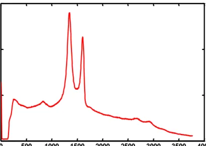
Figure 5.3: Raman spectrum of exfoliated graphene oxide ... 52
Figure 5.4: C-V characteristics of n-type control sample... 53
Figure 5.5: C-V characteristics of p-type control sample... 53
Figure 5.6: C-V characteristics of the samples with/without surface functionalization ... 55
Figure 5.7: Hysteresis window of p-type graphene flash memory device ... 56
Figure 5.8: Hole storage performance of graphene flash devices for varying bias voltages ... 57
Figure 5.9: Retention characteristics of p-type graphene flash devices ... 58
Figure 5.10: Program transient characteristics of p-type graphene flash devices ... 58
Figure 5.11: Memory transfer characteristics of p-type graphene falsh device
under written and erased conditions. ... 59
Figure 5.12: Hysteresis window of n-type graphene flash memory device ... 60
Figure 5.13: Retention characteristics of n-type graphene flash devices. ... 61
Figure 5.14: Program transient characteristics of n-type graphene flash devices. ... 62
Figure 5.15: Hysteresis window of p-type SiN flash memory device. ... 63
Figure 5.16: Hole storage performance of SiN flash devices for varying bias voltages. ... 64
Figure 5.17: Retention characteristics of p-type SiN flash device. ... 65
Figure 5.18: Program transient characteristics of p-type SiN flash devices... 65
Figure 5.19: Hysteresis window of n-type SiN flash memory device. ... 66
Figure 5.20: Retention characteristics of n-type SiN flash device. ... 67
Figure 5.21: Program transient characteristics of n-type SiN flash devices... 68
Figure 5.22: Band diagrams for samples with (a) graphene nanosheets and (b) Si-rich nitride as charge-trapping mediums. ... 69
Figure 5.23: Comparision of hysteresis window for electron storage. ... 70
Figure 5.24: Retention characteristics of samples with graphene trapping layer and SiN trapping layer for electron storage. ... 71
Figure 5.25: Program Transient characteristics of samples with graphene trapping layer and SiN trapping layer for electron storage. ... 72
Figure 5.26: Comparision of hysteresis window for hole storage. ... 73
Figure 5.27: Hole storage performance of samples with graphene trapping layer and SiN trapping layer for varying bias voltages. ... 73
Figure 5.28: Retention characteristics of samples with graphene trapping layer and SiN trapping layer for hole storage. ... 74
Figure 5.29: Program transient characteristics of samples with graphene trapping layer and SiN trapping layer for hole storage. ... 75
Figure 5.30: Device structure for graphene flash device with AlN as charge storage medium. ... 76
Figure 5.32: Band diagram for samples with AlN as the tunnel layer [94, 95]. 79 Figure 5.33: Hysteresis window of graphene flash memory device with AlN as the tunnel layer. ... 80 Figure 5.34: Electron storage performance of samples with graphene trapping layer and AlN tunneling layer for varying bias voltages. ... 80 Figure 5.35: Retention characteristics of graphene flash device with AlN tunneling layer ... 81 Figure 5.36: XPS results of 7nm-thick AlN film deposited on Si(100). ... 82 Figure 5.37: Program transient characteristics of graphene flash device with AlN tunneling layer. ... 83 Figure 5.38: Memory transfer characteristics of graphene flash device with AlN tunneling layer under written and erased conditions. ... 83
List of Tables
Chapter 1
Introduction
Flash memory technology has recently gained much attention with the growing demand of non-volatile memories for mobile electronic devices. The conventional flash memory technology is composed of a MOSFET structure with a continuous floating gate (FG) as the charge storage medium. The basic operation principle of FG flash cell is based on the threshold voltage shift as a result of injected electrons in the charge storage medium. High retention rate, low power consumption, high density and high endurance are the desired features of a flash memory device.
As the dimensions scaled down, the FG technology encounters serious problems such as lateral charge leakage into drain or source regions, and complete charge loss because of pinholes and defects in the tunnel layer. Charge-trapping flash memory structures are proposed to overcome the drawbacks of scaled FG cells. In charge-trapping flash memories, the charge storage medium consists of a large number of electrically isolated traps. Nanoclusters in Si-nitride, semiconductor nanocrystals (Si, Ge etc.) and metal nanocrystals (Co, Ni, Al, Au, Ag etc.) are utilized as discrete traps. Discrete charge storage nodes prevent lateral charge leakage and allow further scaling of the tunnel oxide resulting in direct tunnelling mechanism. Direct tunnelling mechanism is desirable in flash technology to avoid oxide degradation due to
Fowler-Nordheim tunnelling and hot electron injection. Moreover, it allows faster write/erase speed at low operating voltages. The use of discrete charge-trapping medium offers high endurance, low power consumption and fast operation in high density memory applications.
Leakage current increases exponentially as the gate oxide gets thinner, causing reliability problems in flash memories. Various materials with high dielectric constants are proposed as tunnel oxide and blocking oxide in flash memory technology. With the application of high-k dielectrics, the leakage current is significantly suppressed due to increased physical dielectric thickness. High-k dielectrics in flash cells enhance the write/erase speed without degrading the data retention performance. To further enhance the charge injection current and the retention rate, charge storage medium should provide great number of available states in deep energy levels. High-k dielectric flash devices with dense nanocrystals exhibit improved retention performance and faster operation.
This thesis investigates the charge storage property of graphene in flash memory applications and the effect of atomic layer deposited tunnel dielectrics on memory performance. For comparing graphene flash memories, identical flash cells with Si-rich nitride layer as the charge-trapping medium are fabricated and characterized. Our motivation is to improve the performance of the existing flash technology with the use of high-k dielectrics instead of SiO2 as
tunnel/control barrier and graphene as charge storage medium.
This thesis is organized as follows: Chapter 2 includes theoretical preliminaries and basic concepts in flash memory devices. Chapter 3 addresses the promising solutions to the scaling issue in modern flash technology, including the usage of nanocrystals, ALD-grown high-k dielectrics and graphene. Chapter 4 provides detailed explanation of fabrication process and characterization methods. In Chapter 5, performance of fabricated graphene flash memories and detailed comparison with Si-nitride based flash memories
are presented. Chapter 6 concludes the thesis by summarizing the results and provides future work in this direction.
Chapter 2
Device Physics
2.1 Overview of Non-Volatile Memory
Memory is an inherent crucial component of any information processing system. Various types of memories find application in different parts of modern computer systems. Solid state memories offer high density, low power and no mechanical components. Memory devices can be classified into two main types, volatile and non-volatile. A volatile memory loses the information when the power is off. Static Random Access memory (SRAM) and Dynamic Random Access Memory (DRAM) are the most widely-used types of a volatile memory family. SRAMs offer fast writing and reading operations and DRAMs have denser structure.
Unlike volatile memories, non-volatile memories retain the stored content even if the power is turned off. Non-volatile memories (NVM) can be random access and read only. Read-only Memory (ROM), Erasable programmable read-only memory (EPROM), Electrically Erasable Programmable Read-Only Memory (EEPROM) and Flash are the main types of NVMs. Among all, EEPROMs and Flash memories dominant in applications due to continuous improvement in performance and density. An EEPROM cell consists of two transistors while there is a single transistor in each Flash cell. Due to extra transistor, EEPROMs offer lower chip density compared to Flash memories.
Both EEPROMs and Flash memories require a floating gate layer for charge storage.
In recent years, the share of NVM in semiconductor market is increasing due to portable electronic equipments such as cellular phones, digital cameras, laptops etc. Low operating voltage, high density and high retention performance are the desired features of an ideal NVM. Compared to others, Flash seems to be more advantageous considering the cost and the ability to be programmed and erased many times. In the coming years, as mobile computing becomes more widely used, the demand for flash is expected to increase because of the need for low-cost, low-power, and high-density applications such as solid state hard drives, or expanding storage capacity in cell phones and tablets.
2.2 Performance Considerations of Flash Memories
High retention rate, high density, high endurance and low power consumption are the main features of a desired non-volatile semiconductor memory.
Retention rate is the ability to retain the stored information even without power supply. Non-volatility implies that the flash cell should retain the data for at least 10 years at temperatures near 80°C and after many write/erase cycles. In contrast, volatile memories are needed to be refreshed to prevent from losing the stored data. The refresh cycle is important for power consumption. Memories with high retention rate need lower refresh cycles, which decreases power consumption rate. Retention performance is determined by testing the reliability of a flash cell for nearly - s and extrapolated up to s (approximately
ten years). Moreover, different experiments are also conducted at high temperatures to determine the retention capability of the flash cell.
With the current trend in scaling device dimensions, today’s electronic applications require high-density components. A unit cell that is used to store one bit of information determines the memory density. Flash memories are suitable for high density applications due to single transistor structure in each cell. However, serious problems such as difficulty in lateral charge confinement and neighboring cell disturbance may occur due to scaled dimensions. When lateral dimension of memory cell becomes less than 25 nm, confined charges on FG can leak out into drain or source regions; therefore, such cells may need to be refreshed frequently to retain the data, which is not desired for NVMs. In addition, because of lateral charge leakage, one cell can easily disturb neighboring cells. Therefore, development of new technologies to improve floating gate memories must take into account geometry related effects in the device.
Endurance is another criterion to determine the memory performance. Endurance of a memory cell is referred as the ability to be accessed many times without the degradation of the performance. After many write/erase cycles, oxide defects may occur due to charge injection, which results in degradation of endurance and retention, and also reliability problems due to narrowing of the memory window. For solid state hard drives, endurance values above 105 are desirable, where the data is frequently updated.
Low operating voltages are another desired feature of an ideal NVM. It is possible to reduce power consumption by decreasing oxide thickness between the FG and the channel. However, stored charges can leak into the channel easily when the tunnel oxide is scaled down. Moreover, the effect of hot electrons to thinner oxide becomes more serious. As a result, the application of thinner oxide in a Flash cell may reduce both endurance and retention performance.
As outlined above, there are several directions in improvement of floating gate non-volatile memories. A more detailed discussion as given below can help identify routes to improve various qualities of flash NVMs.
2.3 Floating Gate Flash Memories
Floating gate (FG) flash memory is basically a metal-oxide semiconductor field effect transistor (MOSFET) with a poly-silicon FG layer sandwiched between two insulating thin-films. Actually, the storage location is mainly a MOS capacitor with two dielectrics and a FG gate layer between them. The structure of conventional flash cell can be seen in Figure 2.1. FG is a continuous thin-film in which charges are stored. The state of the memory cell is determined by the electrical charge state of the FG. The layer separating FG from the device channel is called as tunnel barrier. The thickness of this layer is generally in the range of 2-10 nm. The FG layer is blocked from the control gate by a control oxide that is used to prevent from discharging through gate contact.
Figure 2.1: Device Structure of Conventional FG Flash Cell
Basic operation principle of a FG flash cell is as follows. When positive bias is applied to the gate, electrons are attracted from substrate through FG tunnel barrier layer via tunneling and trapped on the FG when the gate bias is removed. Negative bias causes the lowering of the barrier and facilitates escape
of electrons back to the substrate. The amount of charge stored on FG results in threshold voltage shift of the underlying transistor. Generally, neutral or positively charged state is defined as logical "1" and programmed or negatively charged state is referred as logical "0". Fowler-Nordheim (FN) and hot electron injection are the most frequently used mechanisms for charging and discharging. Compared to direct tunneling, these mechanisms are faster; however, they cause damage in the oxide layer due to high fields, which degrades endurance and retention performance of the flash cell. Thickness and quality of each oxide layer are also crucial to guarantee both non-volatility and program/erase repeatability. The information is preserved as long as the charges are trapped of FG. For a conventional flash cell, it is expected to retain the data for at least 10 years at temperature range of -40°C and 125°C [1]. Conductive paths along dielectrics may cause trapped charges on FG to tunnel to substrate or to gate; therefore, defect-free oxides are necessary for high performance flash applications.
D. Kahng and S. M. Sze suggested the use of FG for charge storage for the first time in 1967 [2]. The first proposed structure for non-volatile MOS memory is as follows. A metal conducting layer as FG is sandwiched between a thin insulator as tunnel oxide and a thick insulator that isolates the FG from the gate metal. This memory cell is called as MIMIS (metal-insulator-metal-insulator-semiconductor). Extremely thin oxide layer (< 5 nm) allows direct tunneling mechanism for programming. The main drawback of this structure is that all stored charges in metal layer can leak off in case of any pinhole in the tunneling oxide. Hence, there is a reliability problem with MIMIS cell. Increasing the thickness of tunneling oxide and replacing conducting layer with a dielectric without losing the capture probability would be the possible solutions to MIMIS structure.
The first improvement to reliability problem of MIMIS cell was first suggested by Wegener in 1967 [3]. Wegener proposed to replace conducting
layer and the insulator on top it with a nitride layer. This structure is referred as MNOS (metal-nitride-oxide-semiconductor). Nitride layer is composed of large number of traps for both electron and hole storage. Since individual trapping centers are separated from each other, any pinhole in thin tunnel oxide will not cause complete discharging. Applying high positive voltage to gate metal, electrons tunnel from silicon conduction band (CB) to nitride CB and are confined in nitride traps, causing positive shift in threshold voltage. Conversely, high negative bias is applied to erase the cell, resulting in negative threshold voltage shift.
Floating gate Avalanche injection MOS (FAMOS) was suggested by Frohman-Bentchkowsky in 1971 [4-7]. In FAMOS cell, a poly-silicon FG surrounded by a thick oxide is used as charge storage layer. The programming mechanism is mainly based on the creation of highly energetic electrons by drain avalanche plasma. On the other hand, UV or X-ray radiation can be utilized to erase the cell. FAMOS cell was the first structure that is compatible with mass production.
2.4 Charge-Trapping Flash Memories
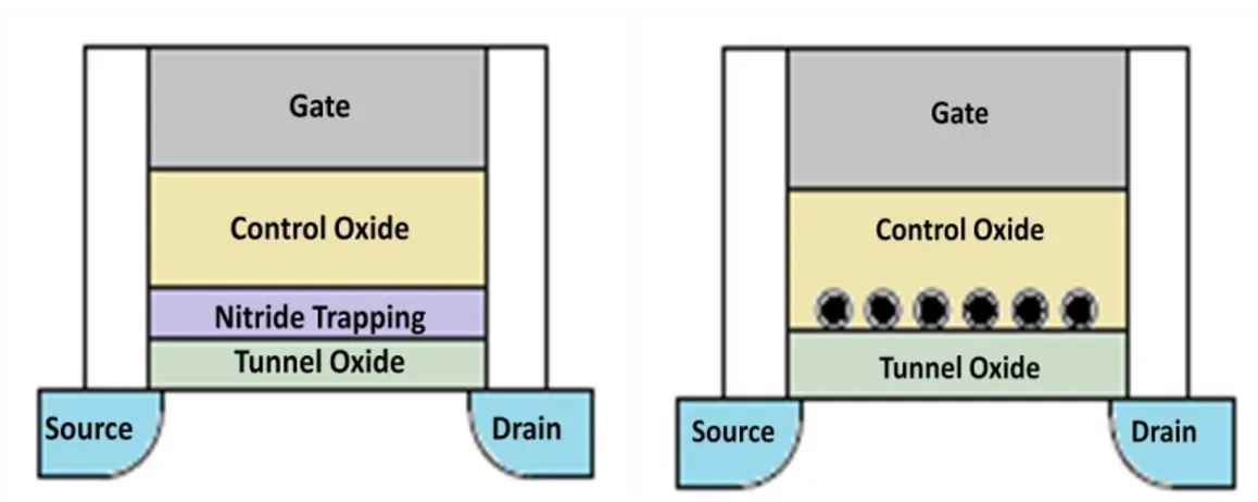
The main distinguishing feature of a charge-trapping flash memory is a discontinuous charge storage medium that contains a large number of electrically isolated traps. The cross-section of charge-trapping cells can be seen in Figure 2.2. Charges are stored in discrete traps, preventing from lateral charge leakage. Nitride films, semiconductor nanocrystals and metal nanocrystals can be used as charge-trapping layers.
Figure 2.2: Device Structures of SONOS and Nanocrystal Flash Cells
The application of discontinuous layer as charge storage medium allows for the reduction of tunnel oxide thickness. In charge-trapping devices, direct tunneling mechanism can be used for charging and discharging because of ultra-thin tunnel oxide. Charge-trapping devices gain some advantages over floating gate memories due to direct tunneling mechanism. One of the main advantages is the life-time of the memory cell is increased since direct tunneling does not degrade the oxide as do Fowler-Nordheim or hot electron injection mechanisms. Another advantage of direct tunneling mechanism is to allow faster program/erase operations. In addition, retention rate of nanocrystal memories is less prone to oxide defects compared to a continuous floating gate memory since there is no lateral conduction between trap centers. Although charge-trapping memories can offer high endurance, low power consumption and fast program/erase speed at high-density memory applications, the distribution and the size of nanocrystals are both crucial to determine device performance.
2.5 MOS Physics
A nanocrystal flash cell can be modeled as a one-dimensional metal-oxide-semiconductor (MOS) capacitor since thick dielectric electric isolates the nanocrystals laterally and the electric field is applied along gate-to-substrate
direction. Size, shape and distribution of nanocrystals, interfacial traps, oxide defects should be carefully analyzed to determine the electrostatic characteristics of a nanocrystal flash memory. To examine the electrical properties, MOS capacitor physics should be studied.
MOS capacitor is the main structure of a single flash cell. A MOS capacitor is composed of a dielectric layer sandwiched between a doped silicon substrate and a metal contact. An ideal MOS capacitor has no charge-trapping centers in the oxide and at oxide/semiconductor interface. Moreover, for an ideal MOS structure, the metal work function should be equal to the semiconductor work function. Leakage current under all static conditions is assumed to be zero in an ideal MOS.
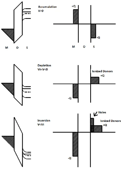
According to applied voltage, MOS capacitor has three biasing regions, accumulation, depletion and inversion; all of which will be studied over an ideal n-type MOS.
2.5.1 Accumulation
When positive voltage is applied, Fermi level (EF) of the metal is lowered
relative to EF of semiconductor, causing a positive slope in the energy band
diagram. Excessive positive charges placed in gate electrode and this positive bias should be balanced by the electrons at the interface. In accumulation region, the total capacitance is the result of an oxide capacitance.
2.5.2 Depletion
The application of small negative voltage to n-type MOS capacitor slightly raises EF of metal with respect to EF of semiconductor. The concentration of
electrons on the gate contact increases, causing the repulsion of majority carriers from the interface. Electron concentration is becoming less than the doping
concentration of Si substrate as the bias voltage is decreasing. The total capacitance is the serial combination of two parallel-plate capacitors, oxide capacitance and depletion capacitance. The depletion capacitance decreases with the increase of depletion thickness.
2.5.3 Inversion
When large negative voltage applied, bands at the interface bend more and depletion width reaches the maximum value. Hole concentration at the surface gets larger than the intrinsic carrier concentration. At low frequencies, minority carriers can follow the ac signal and total capacitance approaches to oxide capacitance value as the negative bias becomes larger. On the other hand, holes in the inversion layer cannot follow the ac signal at high frequencies. Then, the total capacitance will be equal to serially connected oxide capacitance and depletion capacitance.
Band diagrams and charge distributions of each biasing regions including flat-band condition for an ideal n-type MOS capacitor are demonstrated in Figure 2.3.
Figure 2.3: Energy band diagrams and corresponding block charge diagrams in an ideal n-type MOS capacitor.
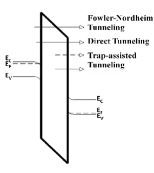
2.6 Tunneling Mechanism
An ideal insulator does not allow any leakage current. But, when high electric field is applied on a thin dielectric layer, charges will pass through the dielectric. Tunneling mechanism is explained as the propagation of a particle through a
potential barrier that it could not pass according to classical view. Tunneling depends on the barrier height, availability of the states and applied electric field. Direct tunneling, Fowler-Nordheim tunneling and trap-assisted tunneling are the tunneling mechanisms to explain charging/discharging of a flash cell, shown in Figure 2.4.
Figure 2.4: Tunneling Mechanisms
2.6.1 Direct Tunneling
Direct tunneling mechanism is referred as the propagation of electrons through the barrier without using the conduction band of the dielectric. It becomes dominant for the dielectrics with a thickness below 5 nm. Direct tunneling is temperature-dependent. It increases exponentially as the decrease of oxide thickness. It does not dependent on the electric field across the dielectric. Direct tunneling does not create oxide defects after repeated cycle operations [8].
2.6.2 Fowler-Nordheim Tunneling
Fowler-Nordheim (FN) tunneling is a quantum mechanical mechanism in which electrons can propagate through the barrier by passing the conduction band of the oxide. The probability of FN tunneling increases exponentially as the electric field in the oxide layer increases [9].
2.6.3 Trap-assisted Tunneling
Oxide defects and interface traps give rise to two-step tunneling mechanisms. Trap-assisted tunneling becomes significant after many write/erase cycles in EEPROMs and flash memories. Due to repeated high stress, the tunneling current increases at low voltages. This is regarded as stress induced leakage current (SILC). SILC is generally accepted as the main reason for the degradation of oxide quality and retention performance in NVMs [10]. SILC was examined for MOS capacitors and EEPROMs in recent studies [11-13]. Single defect in a thick oxide would not be sufficient to initiate a leakage current. However, the existence of several traps can create large SILC and results in gate oxide breakdown.
Chapter 3
Possible Solutions to the Scaling Issue
3.1 Nanocrystal Flash Memory
Floating gate (FG) flash memories encounter major problems as the flash gate stack is scaled down, explained in Chapter 2.In recent years, various materials as charge-trapping layer and high-k dielectrics as tunneling and blocking layers are proposed to overcome scaling issue of the conventional FG memory. One possible solution is to create a memory structure that stores charges in discrete-traps, such as SONOS type memory and nanocrystal memory [14, 15].
The structure of a nanocrystal cell resembles conventional FG memory. The main difference is that charges are not stored in a continuous FG, but in nanocrystals or natural traps of a nitride layer. Those discrete charge-trapping centers allow thinner tunnel oxide thickness without a drastic decrease in the retention performance.
In a FG cell, oxide defects in the tunneling layer may form a conductive path the channel and the FG, which may cause full discharge of stored charges. On the other hand, nanocrystal memories can preserve most of the charge and improve the retention capability since they are stored in discrete traps and such a conductive path may discharge only a small number of nanocrystals. Therefore,
charge-trapping flash memories offer better scalability of the tunnel oxide thickness without retention degradation.
Another major benefit of charge-trapping memories is to allow multi-bit storage due to localized charge storage mechanism [16]. By injecting the charge through channel hot electron (CHE) to the source, to the drain or to the both sides and reading on only one end, it is possible to obtain multi-bit storage mechanism in a single cell, which has a great importance to increase the data density.
The application of nanocrystals as charge-trapping medium seems to be advantageous. They require the use of well-known materials and CMOS-compatible fabrication steps since they have a similar structure to the conventional FG.
3.1.1 Semiconductor Nanocrystal Preparation Methods
The fabrication of semiconductor nanocrystals embedded in a MOS structure has been commonly studied. There are four major methods of nanocrystal preparation in non-volatile memory technology, which are the chemical vapor deposition (CVD) growth, the non-stoichiometric layer deposition, ion-beam synthesis and the layer-by-layer growth.
Si and Ge nanocrystals embedded in a dielectric matrix have been widely used in nanocrystal memory technology. In general, high temperature annealing process is required to complete nanocrystal formation. Ion implantation of Si and Ge in SiO2 matrix is the most frequently used method. This method is based
on implantation of Si or Ge into SiO2 with low energies and post-implant
annealing at high temperatures (>900ºC). At layer-by-layer growth technique, a thin amorphous Ge or Si layer is deposited by e-beam evaporation or thermal evaporation system, and then high-temperature annealing process is applied to
the sample. Si or Ge thin layer is either oxidized or covered by another dielectric layer to complete nanocrystal formation.
Another method of preparation is the deposition of Si-rich SiOx or SiNx
layer by plasma enhanced chemical vapor deposition (PECVD) and subsequent high-temperature annealing. Iacona and coworkers showed that Si nanoclusters with a diameter between 1.4 nm and 4.2 nm are formed after high-temperature annealing of PECVD-deposited Si-rich SiO2 films [17]. The study of Sung et al.
studied the formation of Si nanocrystals embedded in amorphous SiNx films
grown by PECVD at 250ºC [18]. The size of Si nanocrystals varies from 2.1nm to 6.1 nm as altering deposition parameters [18, 19]. Further post-annealing is not applied to the Si-rich oxide and nitride films deposited by PECVD.
CVD is recently the most frequently used technique to form self-assembled nanocrystals in memory applications. The crucial point of this method is to control the initial nucleation of nanocrystals on top of a dielectric. The study of Ammendola et al. seems to be promising to obtain uniformly-distributed Si quantum dots incorporated in a thin SiO2 layer with low-pressure CVD
(LPCVD). The average size of Si quantum dots was determined as 4-6 nm [20].
3.1.2 Metal Nanocrystals
The application of metal nanocrystals as charge-storage layer is also promising because metal nanocrystals offer selectable work function and high density of states. In general, the fabrication of metal nanocrystals is based on the deposition of a thin metal layer by evaporation or sputtering techniques and post-deposition annealing.
Lee et al. demonstrated the charge storage property of Au, Ag and Pt nanocrystals in EEPROM devices [21]. A thin layer of Au, Ag and Pt was deposited o a direct tunneling oxide by e-beam evaporation and subsequently
annealed at 1000ºC. The size and the distribution of metal nanocrystals could be controlled with evaporation and annealing conditions. Besides the study of Lee et al., the charge-trapping property of various metal nanoparticles such as Co, Mo, Ni, TiN and Al nanocrystals were investigated [22-28].
Metal with high work functions are desirable for memory applications because higher effective potential well depth with respect to Si conduction band improves both retention performance and operation speed of the memory. Metal nanoparticles are crucial for engineering of effective potential well depth (deff).
The energy band diagram of a flash cell with metal nanoparticles can be seen in Figure 3.1. High deff offers lower barrier for writing and longer barrier for
retention. Thus, fast write/erase speed with improved retention can be achieved with metal nanocrystals as charge storage nodes.
Figure 3.1: Energy Band Diagram of a Flash Cell with Metal Nanocrystals
Au and Pt have higher work function compared to Co, W, Ag, Al and Ni; as a result, they exhibit better memory performance. However, the application of Au and Pt nanoparticles does not seem to be a cost-effective solution in memory technology. There have been many reports on metal species with high work functions such as W5Si3, NiSi2, CoSi2 nanocrystals to enhance the memory
also offer multi-bit storage mechanism. 2-bits per cell metal nanocrystal memory and 4-bits per cell with quad source/drain devices were reported [33, 34].
3.1.3 Basic Principle of Operation
In conventional flash memories, data storage is mainly based on the threshold shift of FETs due to stored charges. During programming, charges are tunnelled from the channel to the FG. Reading operation is dependent on the measurement of source-drain current. Tiwari et al. explained the charge storage mechanism of nanocrystal flash memories as follows [35]. Reverse bias applied to the gate causes the injection of electrons into the nanocrystals. Conductance of the inversion layer is reduced because of the screening effect of the trapped charges in nanocrystals, causing a shift in the threshold voltage of the FET.
Write/Erase speed and operation voltage are both based on the injection current between the channel and the charge-stored medium. The injection current is exponentially dependent on the electric field across the tunnel oxide for FN tunneling mechanism.
A nanocrystal flash cell can be modelled as a serially connected three parallel plate capacitors. The capacitance of a parallel-plate capacitor is dependent on the permittivity of the dielectric between two plates, the thickness of the dielectric and the area.
When there is no charge stored in the flash memory, the electric field in the bottom oxide can be found as
where
: Applied gate voltage
: Electric field in the tunnel oxide : Dielectric constant of the tunnel oxide : Tunnel oxide thickness
: Dielectric constant of the control oxide : Control oxide thickness
The electric field in the tunnel oxide is a function of the thickness and the dielectric constant of both tunnel oxide and control oxide layers. The decrease in the ratio enhances the electric field in the tunnel oxide. If the control oxide
with a higher dielectric permittivity with respect to the tunnel oxide is used in the gate stack, the programming time duration or the operation voltage will decrease.
Taking into consideration that nanocrystals are the only charge storage nodes and exactly one electron is stored in each nanocrystal, flat band voltage shift is given as [35]
(3.2)
The charge density, , can be directly calculated as
(3.3)
where
: Charge density in nanocrystal medium
: Flat band voltage shift
: Control oxide thickness
: Nanocrystal medium thickness : Dielectric constant of Si
3.1.4 Challenges of Nanocrystal Memories
Although nanocrystal memories is regarded as a solution to scaling issue in conventional FG technology, there still exist major challenges that should be overcome. First of all, the memory performance of nanocrystal-based flash cells is directly affected by the size, the shape and the distribution of nanocrystals. The nanocrystal size must be around 3-4 nm due to carrier confinement effects. When more than one electron is stored in a single nanocrystal, the barrier potential for the electron occupying the highest energy level will reduce due to the increase in energy level separation according to the given formula assuming the nanocrystal shape is a perfectly symmetric sphere [36].
(3.4)
where
: Energy separation
: Capacitance of a spherical nanocrystal
d : Diameter of the nanocrystal
: Dielectric constant of the nanocrystal
In addition, the density of nanocrystals should be at least to obtain an appropriate shift in threshold voltage. Moreover, the separation between two neighboring nanocrystals is also significant to prevent lateral current flow. Generally, nanocrystals are formed by thermal annealing process, rather than by patterning. Thus, it becomes challenging to produce nanocrystals with a certain size, shape and distribution in each individual memory cells.
The use of metal nanoparticles in charge-trapping memories has been also receiving attention since metal nanoparticles offer large density of states around the Fermi level and high work function. Metal nanoparticle memories show improved retention and greater charge storage capability compared to semiconductor nanocrystals due to the deeper effective potential well formed between the metal and the conduction band of the semiconductor. However, the formation of metal nanocrystals is usually required high-temperature process. They can easily diffuse into other layers during thermal annealing. Therefore, they create defects and conductive paths in the tunnel oxide and the control oxide. As a result, non-volatile memories with metal nanocrystals may have reliability problems. Moreover, flash cells with Au nanoparticles as charge storage nodes exhibit better performance due to its higher work function. However, the Au is considered as a non-CMOS compatible material.
3.2 High-k Dielectrics
Modern semiconductor technology requires high-density and low-power applications. In recent years, there have been many applications on possible solutions to overcome challenges arising from scaled dimensions. Silicon-based technology dominates modern electronic devices because of the excellent interface at Si / SiO2. Although other semiconductors such as Ge, GaAs, InGaAs
offer greater transport properties, low-trap density at the interface of Si and its native oxide, SiO2 is considered as one reason that silicon-based FETs are the
basis of modern electronics.
Further scaling of SiO2 beyond 10 nm brings problems due to two main
reasons. First of all, leakage current rises exponentially as the gate oxide gets thinner because of quantum mechanical tunneling of carriers through such a thin SiO2 layer. The leakage current not only reduces the reliability of the device, but
also creates oxide defects after repeated cycles of operation. The second reason is that the SiO2 loses its bulk electronic properties when its thickness is scaled
down to 0.7 nm. Because of such problems arising from the scaling issue, semiconductor technology is looking for new materials that form low-trap density on top of Si and offer equivalent electrical properties of a scaled SiO2.
High-k materials are regarded as an alternative solution to scaling issue to suppress the leakage current without reducing the oxide capacitance. The reduction of the leakage current is achieved by increasing the physical thickness of gate oxide, which is explained with equivalent oxide thickness (EOT). The EOT represents the electrical thickness of a dielectric that corresponds to the equivalent capacitance of a physically thinner SiO2 layer. The EOT is given as
(3.5)
where is the thickness of the high-k layer, and are the
relative dielectric constants of SiO2 and high-k dielectric.
Band gaps and band offsets of various high-k materials can be seen in Figure 3.3 [37]. A high-k material with large band gap and high band offsets for both electrons and holes are required for an alternative gate dielectric. The inverse relation between the dielectric constants and the band gaps is shown in Figure 3.4 [38].
Figure 3.2: Band gaps and band offsets of various high-k materials [37].
Figure 3.3: Inverse relation between band gap and dielectric constant of various high-k materials [38].
The first motivation for the replacement of SiO2 with a high-k material was
to reduce the leakage current. Much work has focused on the leakage current measurements of devices with various high-k gate dielectrics. A transistor with Al2O3 as a gate dielectric was reported in 2000 [39]. Further studies showed that
the high-k dielectric layer as a gate oxide causes a flat band voltage shift in capacitance-voltage measurements, indicating the existence of oxide charges and traps. Studies on thermodynamic stability of the high-k materials onto Si have also reported [40-42]. BeO, ZrO2 and HfO2 are shown to be
thermodynamically more stable than Al2O3, TiO2 and Ta2O5 [43].
Gritsenko et al. compared the simulated write/erase characteristics of SONOS devices with SiO2, Al2O3 and ZrO2 as a blocking oxide. They concluded
that the application of high-k as a control oxide reduces the operation voltage or the write/erase speed from 1ms to 10µs [44]. Moreover, interfacial properties of high-k materials with Si in flash applications were studied [45].
The use of high-k materials as a tunnel oxide in flash memories is advantageous over SiO2 gate oxide. First, it improves the write/erase speed. The
charge injection mechanism of most flash memories is based on FN tunneling and hot electron injection. These tunneling mechanisms are dependent on the potential barrier height between the Si substrate and the tunnel oxide. Actually, larger barrier height requires higher voltage operation or longer programming duration. Most high-k dielectrics form lower barrier height on Si, allowing faster operations or low-voltage applications. The second is the improved retention rate. Since high-k dielectrics are physically thicker than a SiO2 layer to achieve
the EOT, SONOS with a high-k dielectric as a tunnel oxide can exhibit better retention performance.
Dana et al. proposed a model that explains the charge/discharge dynamics of nanocrystal flash memories and studied the effect of dielectric properties on memory performance [46]. In this study, the figure of merit (FOM) is defined as
(3.6)
where and denote the retention and the charging times. The FOM is calculated for various high-k dielectric materials with same EOT and other parameters that effect charge/discharge dynamics such as nanocrystal size and distribution, write voltage, and gate work function are kept unchanged, given in Figure 3.4.
Figure 3.4: FOM for various high-k materials for nanocrystal diameter of 6 nm, write voltage of 10 V, and EOT of 4 nm [46].
The use of materials with higher dielectric constants improves the FOM, leading to enhanced retention rate and decreased charging time. Since high-k materials provide larger physical thickness, the escape tunnelling current is significantly decreased. Charging time is also improved as a result of smaller conduction band offset of the high-k material on Si.
3.2.1 Reliability Issues of High-k Dielectrics
Although high-k dielectrics are regarded as a solution to scaling issue of SiO2
gate oxide, they have various disadvantages that directly affect the performance and the reliability of the device.
One major problem for the integration of high-k dielectrics to CMOS technology is the presence of dipoles and defects at Si/high-k interface. Capacitance-voltage measurements of a MOS capacitor with a high-k layer demonstrate that the flat band voltage is shifted from the ideal position, proving the existence of uncompensated charges and dipoles in the high-k oxide. Diffusion of oxygen through the film and formation of SiOx layer at the interface
was observed in most high-k oxides including Al2O3, ZrO2 and HfO2. To prevent
oxygen diffusion from gate electrode, poly-Si gate is replaced with a metal electrode such as TiN [47]. At this point, the metal contacts should have appropriate work functions and thermal stability at temperatures required for CMOS technology.
Secondly, mobility degrades as the thickness of gate stack decreases. The reason for this is explained as the coupling of soft phonon modes in the dielectric with channel electrons [48]. It is probable that charge trapping and fixed charges in high-k films are responsible for lower carrier mobility. Moreover, it was reported that the mobility becomes higher when the thickness of the interfacial SiOx becomes more than 1nm by thermal treatments. Forming
gas annealing at high temperatures and O3 surface treatments were carried out to
reduce interfacial defects [49-51].
In addition, another challenge with the integration of high-k dielectrics is the presence of fast charge trapping and detrapping. Hysteresis phenomena and threshold voltage instability in MOSFETs with HfO2 was reported [52]. It was
observed that threshold voltage shift depends on the HfO2 thickness and post
deposition annealing conditions.
The thermal stability of high-k materials is also crucial for device performance because conventional CMOS technology needs for high-temperature steps. At high high-temperatures, ultra thin high-k layers cannot prevent O2 diffusion through Si surface and there occurs SiO2 growth at the interface [53,
54].
3.3 Graphene
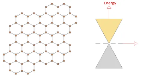
Graphene is a one-atom thick material made of carbon atoms that are arranged in honeycomb order. In 2010, graphene was worth of Nobel Prize since it is considered as one of the most promising material ever discovered. Graphene is regarded as a unique material because of its electrical, thermal, mechanical, optical and chemical properties. Graphene is one of the strongest and the most conductive material ever known. The unique properties of graphene make it the most promising material for electronic applications, including transistors, sensors, composite materials and flexible electronics. Especially for transistor technology, graphene is proposed as a new solution that can be used to further Moore’s Law.
The main challenge is the growth of high quality graphene layers. Graphene films are desired to be uniform with minimal roughness and few defects. One method of graphene deposition is metal exfoliation or scotch-tape method [55]. In this method, the starting material is commercially available highly ordered pyrolytic graphite (HOPG). To mechanically exfoliate graphene on a substrate, a piece of sticky tape is used to peel graphene layers from HOPG and sticky tape is removed slowly from the substrate. Although high-quality graphene layers with few defects are obtained, this method would not seem to be applicable to mass production. In addition, graphene is deposited in a small area
and number of graphene layers varies. The number of graphene layers is also a crucial issue in device applications. In recent years, many studies have focused on the fabrication of wafer-sized graphene layers and the interaction of graphene with other materials.
Figure 3.5: Graphene and its band structure
The high mobility and the doping property allow the graphene an alternative material to the silicon technology. Although the graphene has a zero band gap, recent studies showed that bilayer and few-layer graphene introduce a band gap [56]. Many researchers and industrial companies such as Intel and IBM are doing research on field effect transistor with graphene as a channel. The stability of graphene has already moved the attention into one-electron transistors and molecular-sized electronic devices.
3.3.1 Graphene Growth Techniques
The mechanical exfoliation is a simple method to produce graphene flakes with high purity. But, it is not useful for mass production and large-area applications. Besides mechanical exfoliation method, recent techniques are chemical vapor
deposition (CVD), epitaxy deposition and chemical decomposition of graphite oxide.
3.3.1.1 CVD Growth
Chemical Vapor Deposition (CVD) is a technique to deposit solid materials from a gaseous phase at low or vacuum pressure. In CVD, precursor gases are delivered into the reaction chamber at ambient temperatures. As they come into contact with a heated substrate, they react or decompose forming a solid phase and are deposited onto the substrate. The most commonly used material that catalyzes a CVD process is metal. In CVD growth of graphene, organic gases are used to initiate the growth of carbon monolayer. Growth condition can be optimized by changing the gas flow rates, the metal film thickness, the cooling rate and the temperature.
Li and coworkers have demonstrated graphene growth on copper using a mixture of hydrogen and methane gases at temperatures up to 1000°C [57]. One of the major benefits of this method is that it can be integrated to CMOS fabrication technology because 300 nm copper films on silicon wafer is a standard substrate in CMOS technology. They used SEM, TEM and Raman Spectroscopy to determine the uniformity and quality of graphene flakes. The process yielded graphene that was 95% monolayer over an area of 1cmx1cm. Mobility was reported as 4.050 cm2V-1s-1, confirming the high concentration of monolayer graphene. The grown graphene can also be easily transferred to other substrates such as Si/SiO2. This work seems to be promising for
graphene-based applications; however, maintaining chamber pressure during the procedure is a crucial issue due to the gaseous methane. They also reported that graphene growth on copper is self-limited. Growth that proceeded for more than 60 min yielded is similar to growth performed for 10 min. For less than 10 min, SEM images show that copper film is not completely covered. The growth of graphene on Cu foils of varying thicknesses also yields similar structures. Based
on these observations, they reiterated that graphene is growing by a surface-catalyzed process rather than a precipitation process.
A method for the direct CVD of monolayer or few-layer graphene film on dielectric surfaces via a sacrificial copper film was reported [58]. Based on the observation of evaporation of Cu during CVD process, they proposed a new method for graphene growth on insulators by a controlled metal evaporation during or immediately after the catalytic growth. According to metal thickness and duration of CVD process, the areas between metal fingers change in size and shape. It was reported that almost 20 m2 size areas filled with continuous graphene layers. The continuity of the metal film on the surface depends on its thickness, the metal-dielectric wetting properties, the temperature and the time. This method was reported to be applicable to various insulating surfaces including single-crystal quartz, sapphire, fused silica, and silicon oxide. This process could suppress the need for a transfer to a new substrate. Additionally, further improvements on the control of dewetting and evaporation process could result in direct deposition of graphene for large-area electronics.
Rather than copper films, graphene can also be grown on nickel films. The film thickness should be less than 300 nm, preventing from graphite deposition. Graphene is produced on nickel surface using a diluted hydrocarbon gas at ambient pressure and 1000°C [59]. The film is then evaporated by e-beam deposition onto Si/SiO2 substrate. Thermal annealing facilitates the growth of a
nickel film. Nickel film can be etched with chemicals to transfer the graphene layers to another substrate. Direct patterning of graphene film was also demonstrated and this method eliminates the need for post-processing.
The study of Lee and coworkers is mainly based on the idea of graphene growth at low temperatures by plasma enhanced chemical vapor deposition (PECVD) [60]. A methane/hydrogen mixture is utilized to form plasma. Plasma is applied at a pressure of 2 mbar at a process temperature of 450°C. The
substrate with graphene film is then annealed at 900°C and rapidly cooled. This method produces at both top of nickel film and at interface between Si and nickel film. They also observed that annealing does not seem to enhance the graphene film quality; however, they proposed that annealing could be applied to increase the quality of graphene grown at Si/nickel film interface at low temperature processes.
Lee and coworkers further studied on production of wafer scale, high-quality graphene films on Ni and Cu films under ambient pressure and transfer them onto arbitrary substrates by chemical etching of metal layers and polymer-supported transfer onto arbitrary substrates [61]. They used 3-inch SiO2/Si
wafers with 300 nm-thick Ni or 700 nm-thick Cu. They applied a mixture of hydrogen/helium/methane for Cu and a mixture of hydrogen/argon/methane for Ni for 5 min. The samples were then rapidly cooled down to room temperature. They observed that the average number of graphene layers grown on a Ni film ranged from 3 to 8. On the other hand, the monolayer and bilayer graphene grew on a Cu film. In their study, the polymer supports such as PDMS and thermal-release tapes were used to transfer graphene layers.
In case of flexible electronics, it seems to be difficult to grow graphene directly on plastic surfaces due to low temperature melting point of plastic. In a recent process, mechanical rollers are used to transfer graphene film from a thermal release tape to a PET film at 120°C [62]. With roll-to-roll production of 8-inch wafer scale graphene films, commercial production of graphene-based transparent electrodes could be released in the near future.
3.3.1.2 Epitaxial Growth
In epitaxial growth, the substrate acts as a seed crystal and the deposited film will have the similar crystallographic orientations with respect to the substrate. The most popular epitaxial process makes use of a silicon carbide (SiC)
substrate. For large-scale few-layer graphene production, epitaxial growth on SiC by thermal decomposition is receiving much interest. When SiC substrates are annealed at high temperatures, Si atoms selectively desorbs from the surface and the C atoms are left behind naturally form FLG. Because SiC is a wide-band-gap semiconductor, FLG on SiC can serve as a graphene substrate for electronics applications [63]. The two fundamental problems with thermal decomposition are thickness distribution and understanding how the SiC substrate affects physical properties of FLG. In epitaxial growth method, the substrate increases the possibility of achieving a large area of graphene due to the uniform structure of the substrate crystal.
Emtsev and coworkers proposed a near atmospheric pressure method to grow graphene epitaxially from SiC and compare their results with high-vacuum experiments [64]. The authors grew graphene at 676.4 Torr, increasing the temperature, which is necessary for decomposition of the SiC sample. They observed that growth rate increases; however, the surface of the grown graphene improved. To decrease the growth rate, they applied argon to the sample to slow down the Si atoms leaving the surface. Their near-atmospheric method results in the increase of the mobility by a factor of 2 compared to high-vacuum experiments. This method seems to be promising due to importance of growth rate control in epitaxial methods.
3.3.1.3 Chemical Techniques
Chemical exfoliation of graphite to form graphene monolayer has been a promising method for mass production. The starting point for the fabrication of reduced graphene oxide (rGO) thin films is the oxidation of graphite. For electronic and optoelectronic applications, GO should be reduced to become electrically conductive. Synthesis of graphite oxide can be achieved by placing graphite in concentrated acid. Hummers proposed a less dangerous process of graphite oxidation with a mixture of sodium nitrate, potassium permanganate
![Figure 3.2: Band gaps and band offsets of various high-k materials [37].](https://thumb-eu.123doks.com/thumbv2/9libnet/5778543.117271/39.892.198.794.190.576/figure-band-gaps-band-offsets-various-high-materials.webp)
![Figure 3.4: FOM for various high-k materials for nanocrystal diameter of 6 nm, write voltage of 10 V, and EOT of 4 nm [46]](https://thumb-eu.123doks.com/thumbv2/9libnet/5778543.117271/41.892.283.676.447.779/figure-fom-various-materials-nanocrystal-diameter-write-voltage.webp)