I. INTRODUCTION
The possibility of altering the spontaneous emission from radiation sources by means of electromagnetic mode distri-butions different from that of free space mode distribution was first predicted in 1946 by Purcell.1This effect has been investigated experimentally in cavities with simple geom-etries, such as plane mirrors and spheres.2,3 Yablonovitch4 proposed a different class of periodic structures, which we now call photonic crystals共PC’s兲, that can be used to control spontaneous emission. PC’s are structures with periodic di-electric constant variations. Periodic didi-electric constant variations lead to electromagnetic band gaps共where there are no propagating electromagnetic modes兲 along certain direc-tions in the crystal.5– 8Absence of modes along certain direc-tions can be used for various applicadirec-tions, such as micro-scopic lasers,9 resonant antennas,10 and optical switches.11
Most of the work devoted to the PC’s up to now have focused on the transmission and reflection properties of PC’s. However, this provides little insight into how a PC modifies the emission properties of a radiating source. The effect of PC’s on the radiation properties of sources have been theo-retically investigated by several authors.13–16,12 Interesting phenomena such as photon-atom bound dressed states,16 nonexponential decay of spontaneous emission near the band edge,15 and strong inhibition of emission and enormous en-hancement of radiation12 have been reported. These works have revealed that PC’s may provide far-reaching control over the spontaneous emission and the radiation dynamics of sources. For instance, spontaneous emission can be en-hanced, suppressed or attenuated in all or certain directions by changing the density of modes.12
Surprisingly, only a few experiments have been reported on the radiation properties of localized sources inside PC’s. Preparation of well defined systems is the major problem for such experiments. Some experiments have been performed to investigate the emission properties of dye molecules em-bedded inside PC’s.17,18These experiments have led to dif-ferent interpretations and are still subject to discussion.19,20 On the other hand, it has been suggested that similar effects such as nonexponential decay rates,21 inhibition of radia-tion,22enormous enhancement at the band edges12and cavity modes23 can be observed at longer wavelength scales.
The effect of PC’s on the radiation of a localized source is encapsulated in local density of states 共LDOS兲, which
de-pends on position and frequency. For a PC, LDOS is propor-tional to the amplitude of the electric field at the position where the source is located. On the other hand, it is inversely proportional to the group velocity of the mode, /k, at
which the source radiates.24In this sense, PC’s provide enor-mous control over the radiation of a source, since for a PC it is possible to find positions with high or low electric-field amplitude and a mode with low or high group velocity. In this paper, we report the radiation properties of a finite-size line source, which we will call hereafter a monopole source, embedded inside a PC.
II. ENHANCEMENT OF RADIATION AND REDUCED GROUP VELOCITIES
In our experiments, we have studied the emission of mi-crowave radiation from a monopole source located inside a PC and a monopole source located inside various defect structures created inside a PC. The monopole source is ob-tained by removing 0.5 cm of the cladding from a coaxial cable and leaving the metal part. The monopole source is then excited by the network analyzer. An HP-8510C vector network analyzer is used in our measurements. HP-8510C network analyzer is capable of measuring both intensity and phase. The phase information obtained from the measure-ment is used to determine the delay time or the photon life-time. The photon lifetime is defined asp⫽/. Here, is the net phase difference between the phase of the electro-magnetic共EM兲 waves propagating inside the photonic crys-tal and the phase of the EM waves propagating in free space for a total crystal length of L. The photon lifetime corre-sponds to the propagation time of the EM waves inside the photonic crystal.25Hence, group velocity is inversely propor-tional to the photon lifetime. The photon lifetime and its physical interpretations have been rigorously studied by Oh-taka et al.26 –29It has been shown that the optical density of modes is directly proportional to the photon lifetime.29
A. Enhanced emission from the monopole at the band edges For a finite PC, the group velocities of the modes at the band edges are expected to be small30–32 and correspond-ingly, the photon lifetimes are expected to be high. Hence it follows that LDOS is high at the band edge modes as LDOS is inversely proportional to the group velocity.
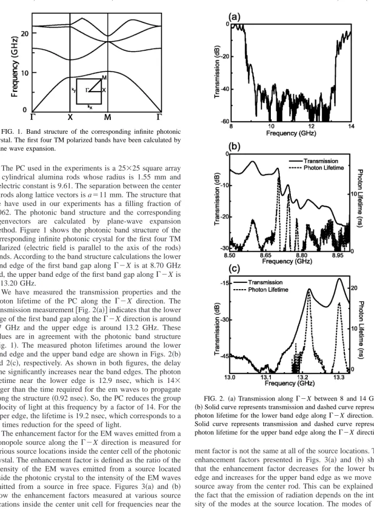
The PC used in the experiments is a 25⫻25 square array of cylindrical alumina rods whose radius is 1.55 mm and dielectric constant is 9.61. The separation between the center of rods along lattice vectors is a⫽11 mm. The structure that we have used in our experiments has a filling fraction of 0.062. The photonic band structure and the corresponding eigenvectors are calculated by plane-wave expansion method. Figure 1 shows the photonic band structure of the corresponding infinite photonic crystal for the first four TM polarized 共electric field is parallel to the axis of the rods兲 bands. According to the band structure calculations the lower band edge of the first band gap along ⌫⫺X is at 8.70 GHz and, the upper band edge of the first band gap along⌫⫺X is at 13.20 GHz.
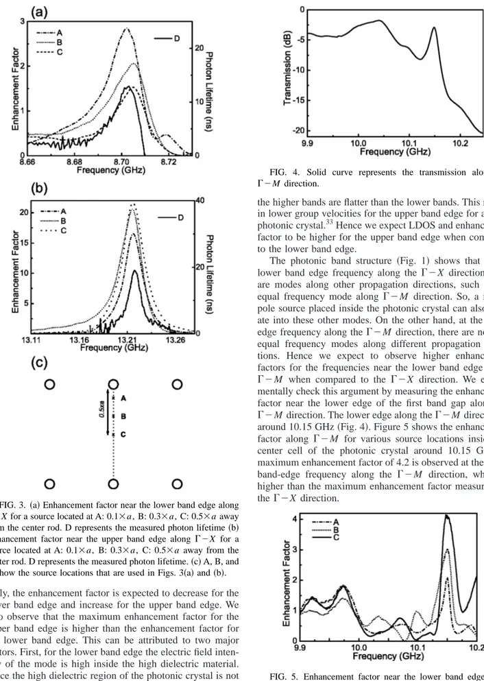
We have measured the transmission properties and the photon lifetime of the PC along the ⌫⫺X direction. The transmission measurement关Fig. 2共a兲兴 indicates that the lower edge of the first band gap along the⌫⫺X direction is around 8.7 GHz and the upper edge is around 13.2 GHz. These values are in agreement with the photonic band structure
共Fig. 1兲. The measured photon lifetimes around the lower
band edge and the upper band edge are shown in Figs. 2共b兲 and 2共c兲, respectively. As shown in both figures, the delay time significantly increases near the band edges. The photon lifetime near the lower edge is 12.9 nsec, which is 14⫻ larger than the time required for the em waves to propagate along the structure共0.92 nsec兲. So, the PC reduces the group velocity of light at this frequency by a factor of 14. For the upper edge, the lifetime is 19.2 nsec, which corresponds to a 22 times reduction for the speed of light.
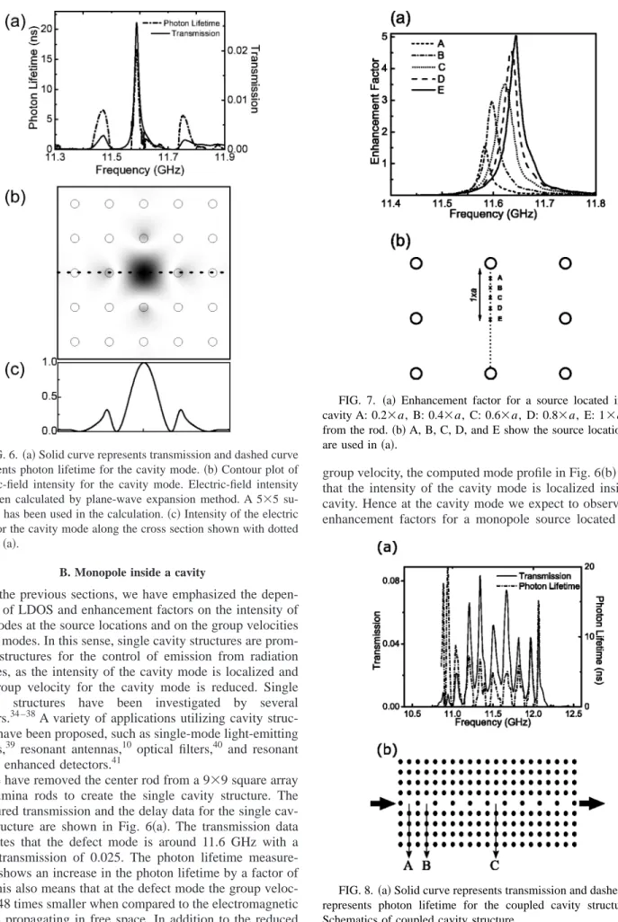
The enhancement factor for the EM waves emitted from a monopole source along the ⌫⫺X direction is measured for various source locations inside the center cell of the photonic crystal. The enhancement factor is defined as the ratio of the intensity of the EM waves emitted from a source located inside the photonic crystal to the intensity of the EM waves emitted from a source in free space. Figures 3共a兲 and 共b兲 show the enhancement factors measured at various source locations inside the center unit cell for frequencies near the lower edge and the upper edge, respectively. The source lo-cations are shown in Fig. 3共c兲. Although enhancement of radiation is expected for the band edge modes, the
enhance-ment factor is not the same at all of the source locations. The enhancement factors presented in Figs. 3共a兲 and 共b兲 show that the enhancement factor decreases for the lower band edge and increases for the upper band edge as we move the source away from the center rod. This can be explained by the fact that the emission of radiation depends on the inten-sity of the modes at the source location. The modes of the lower band edge are dielectric modes, while the modes of the upper band edge are air modes. Hence, as we move the source away from the center rod, LDOS and correspond-FIG. 1. Band structure of the corresponding infinite photonic
crystal. The first four TM polarized bands have been calculated by plane wave expansion.
FIG. 2. 共a兲 Transmission along ⌫⫺X between 8 and 14 GHz.
共b兲 Solid curve represents transmission and dashed curve represents
photon lifetime for the lower band edge along⌫⫺X direction. 共c兲 Solid curve represents transmission and dashed curve represents photon lifetime for the upper band edge along the⌫⫺X direction.
ingly, the enhancement factor is expected to decrease for the lower band edge and increase for the upper band edge. We also observe that the maximum enhancement factor for the upper band edge is higher than the enhancement factor for the lower band edge. This can be attributed to two major factors. First, for the lower band edge the electric field inten-sity of the mode is high inside the high dielectric material. Since the high dielectric region of the photonic crystal is not experimentally accessible, the possible highest enhancement factor cannot be measured for the lower band edge. Second,
the higher bands are flatter than the lower bands. This results in lower group velocities for the upper band edge for a finite photonic crystal.33Hence we expect LDOS and enhancement factor to be higher for the upper band edge when compared to the lower band edge.
The photonic band structure 共Fig. 1兲 shows that at the lower band edge frequency along the ⌫⫺X direction there are modes along other propagation directions, such as the equal frequency mode along ⌫⫺M direction. So, a mono-pole source placed inside the photonic crystal can also radi-ate into these other modes. On the other hand, at the band-edge frequency along the⌫⫺M direction, there are no such equal frequency modes along different propagation direc-tions. Hence we expect to observe higher enhancement factors for the frequencies near the lower band edge along
⌫⫺M when compared to the ⌫⫺X direction. We
experi-mentally check this argument by measuring the enhancement factor near the lower edge of the first band gap along the
⌫⫺M direction. The lower edge along the ⌫⫺M direction is
around 10.15 GHz共Fig. 4兲. Figure 5 shows the enhancement factor along ⌫⫺M for various source locations inside the center cell of the photonic crystal around 10.15 GHz. A maximum enhancement factor of 4.2 is observed at the lower band-edge frequency along the ⌫⫺M direction, which is higher than the maximum enhancement factor measured for the ⌫⫺X direction.
FIG. 3. 共a兲 Enhancement factor near the lower band edge along
⌫⫺X for a source located at A: 0.1⫻a, B: 0.3⫻a, C: 0.5⫻a away
from the center rod. D represents the measured photon lifetime共b兲 Enhancement factor near the upper band edge along ⌫⫺X for a source located at A: 0.1⫻a, B: 0.3⫻a, C: 0.5⫻a away from the center rod. D represents the measured photon lifetime.共c兲 A, B, and C show the source locations that are used in Figs. 3共a兲 and 共b兲.
FIG. 4. Solid curve represents the transmission along the
⌫⫺M direction.
FIG. 5. Enhancement factor near the lower band edge along
⌫⫺M for a source located at A: 0.5⫻a, B: 0.3⫻a, C: 0.1⫻a away
B. Monopole inside a cavity
In the previous sections, we have emphasized the depen-dence of LDOS and enhancement factors on the intensity of the modes at the source locations and on the group velocities of the modes. In this sense, single cavity structures are prom-ising structures for the control of emission from radiation sources, as the intensity of the cavity mode is localized and the group velocity for the cavity mode is reduced. Single cavity structures have been investigated by several authors.34 –38A variety of applications utilizing cavity struc-tures have been proposed, such as single-mode light-emitting diodes,39 resonant antennas,10 optical filters,40 and resonant cavity enhanced detectors.41
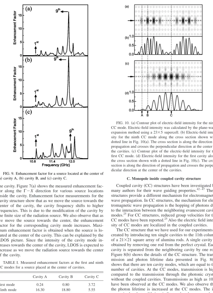
We have removed the center rod from a 9⫻9 square array of alumina rods to create the single cavity structure. The measured transmission and the delay data for the single cav-ity structure are shown in Fig. 6共a兲. The transmission data indicates that the defect mode is around 11.6 GHz with a peak transmission of 0.025. The photon lifetime measure-ment shows an increase in the photon lifetime by a factor of 48. This also means that at the defect mode the group veloc-ity is 48 times smaller when compared to the electromagnetic waves propagating in free space. In addition to the reduced
group velocity, the computed mode profile in Fig. 6共b兲 shows that the intensity of the cavity mode is localized inside the cavity. Hence at the cavity mode we expect to observe high enhancement factors for a monopole source located inside FIG. 7. 共a兲 Enhancement factor for a source located inside a cavity A: 0.2⫻a, B: 0.4⫻a, C: 0.6⫻a, D: 0.8⫻a, E: 1⫻a away from the rod.共b兲 A, B, C, D, and E show the source locations that are used in共a兲.
FIG. 8.共a兲 Solid curve represents transmission and dashed curve represents photon lifetime for the coupled cavity structure. 共b兲 Schematics of coupled cavity structure.
FIG. 6.共a兲 Solid curve represents transmission and dashed curve represents photon lifetime for the cavity mode.共b兲 Contour plot of electric-field intensity for the cavity mode. Electric-field intensity has been calculated by plane-wave expansion method. A 5⫻5 su-percell has been used in the calculation.共c兲 Intensity of the electric field for the cavity mode along the cross section shown with dotted line in共a兲.
the cavity. Figure 7共a兲 shows the measured enhancement fac-tor along the ⌫⫺X direction for various source locations inside the cavity. Enhancement factor measurements for the cavity structure show that as we move the source towards the center of the cavity, the cavity frequency shifts to higher frequencies. This is due to the modification of the cavity by the finite size of the radiation source. We also observe that as we move the source towards the center, the enhancement factor for the corresponding cavity mode increases. Maxi-mum enhancement factor is obtained when the source is lo-cated at the center of the cavity. This can be explained by the LDOS picture. Since the intensity of the cavity mode in-creases towards the center of the cavity, LDOS is expected to increase as we move the radiation source towards the center of the cavity.
C. Monopole inside coupled cavity structure
Coupled cavity共CC兲 structures have been investigated by many authors for their wave guiding properties.42– 47 These structures provide a different mechanism for electromagnetic wave propagation. In CC structures, the mechanism for elec-tromagnetic wave propagation is the hopping of photons due to the interaction between the neighboring evanescent cavity modes.25For CC structures, reduced group velocities for the CC modes have been reported.25Also the electric field inten-sity of CC modes are localized in the coupled cavities.
The CC structure that we have used for our experiments is created by introducing ten single cavities to the 11th column of a 21⫻21 square array of alumina rods. A single cavity is obtained by removing one rod from the perfect crystal. Each cavity is separated from the neighboring cavity by one rod. Figure 8共b兲 shows the details of the CC structure. The trans-mission and photon lifetime data presented in Fig. 8共a兲 shows that there are ten cavity modes, which are equal to the number of cavities. At the CC modes, transmission is high compared to the transmission through the photonic crystal without the coupled cavities. Transmissions as high as 10% have been observed at the CC modes. We also observe that the photon lifetime is increased at the CC modes. The in-crease in the photon lifetime indicates that the group veloci-FIG. 9. Enhancement factor for a source located at the center of
共a兲 cavity A, 共b兲 cavity B, and 共c兲 cavity C.
FIG. 10. 共a兲 Contour plot of electric-field intensity for the ninth CC mode. Electric-field intensity was calculated by the plane-wave expansion method using a 23⫻5 supercell. 共b兲 Electric-field inten-sity for the ninth CC mode along the cross section shown with dotted line in Fig. 10共a兲. The cross section is along the direction of propagation and crosses the perpendicular direction at the center of the cavities. 共c兲 Contour plot of the electric-field intensity for the first CC mode.共d兲 Electric-field intensity for the first cavity along the cross section shown with a dotted line in Fig. 10共c兲. The cross section is along the direction of propagation and crosses the perpen-dicular direction at the center of the cavities.
TABLE I. Measured enhancement factors at the first and ninth CC modes for a source placed at the center of cavities.
Cavity A Cavity B Cavity C
First mode 0.24 0.80 3.72
cavity C are shown in Figs. 9共a兲–共c兲, respectively. The en-hancement factors for the first and ninth CC modes are given in Table I. We observe that when the source is placed either at cavity A or cavity B, ninth CC mode has the highest en-hancement factors, while the first CC mode has the lowest enhancement factor compared to the other CC modes. At cavity A and cavity B, enhancement factors of 16.3 and 18.8 have been observed respectively 共Table I兲. On the other hand, Fig. 9共c兲 and Table I show that when we place the source at cavity C, the enhancement factor for the first CC mode is higher for cavity C, when compared to cavities A and B. This can be explained by the fact that the enhance-ment factor depends on the intensity of electric field at the source location. Since the intensity of the electric field for the ninth CC mode shown in Figs. 10共a兲 and 共b兲 is high at the centers of cavity A and cavity B, we expect higher enhance-ment factors for this CC mode when the source is placed at
showed the enhancement of radiation along with reduced group velocities at the band edges. Moreover, we experimen-tally demonstrated the enhancement of radiation at a single cavity mode and at the CC modes. At the single cavity and CC modes, low group velocities along with high electric-field intensities result in increased enhancement factors. The enhancement factor for a source depends on the group veloc-ity of the mode and on the intensveloc-ity of the electric field at the source location.
ACKNOWLEDGMENTS
This work was supported by a grant from European Union under EU-DALHM project and by a grant from NATO
共Grant No. SfP971970兲. Also, the authors would like to
thank Professor Ezel K. Shaw for her comments during the preparation of the manuscript.
*Electronic address: [email protected] 1E. M. Purcell, Phys. Rev. 69, 681共1946兲.
2P. Goy, J. M. Raimond, M. Gross, and S. Haroche, Phys. Rev. Lett. 50, 1903共1983兲.
3
P. Dobiasch and H. Dehmelt, Ann. Phys.共Paris兲 10, 825 共1985兲. 4E. Yablonovitch, Phys. Rev. Lett. 58, 2059共1987兲.
5K. M. Ho, C. T. Chan, and C. M. Soukoulis, Phys. Rev. Lett. 65, 3152共1990兲.
6E. Ozbay, E. Michel, G. Tuttle, R. Biswas, M. Sigalas, and K.-M. Ho, Appl. Phys. Lett. 64, 2059共1994兲.
7J. D. Joannopoulos, R. D. Meade, and J. N. Winn, Photonic Crys-tal: Molding the Flow of Light共Princeton University Press, Prin-ceton, NJ, 1995兲.
8E. Ozbay, J. Opt. Soc. Am. B 13, 1945共1996兲.
9O. Painter, R. K. Lee, A. Scherer, A. Yariv, J. D. O’Brien, P. D. Dapkus, and I. Kim, Science共Washington, DC, U.S.兲 284, 1819 共1999兲.
10B. Temelkuran, M. Bayindir, E. Ozbay, R. Biswas, M. M. Sigalas, G. Tuttle, and K. M. Ho, J. Appl. Phys. 87, 603共2000兲. 11K. Busch and S. John, Phys. Rev. Lett. 83, 967共1999兲.
12R. Sprik, B. A. Van Tiggelen, and A. Legendijk, Europhys. Lett. 35, 265共1996兲.
13A. A. Asatryan, K. Busch, R. C. McPhedran, L. C. Botten, C. Martijn de Stedrke, and N. A. Nicorovici, Phys. Rev. E 63, 046612共2001兲.
14Virginie Lousse, Pol Vigneron, Xavier Bouju, and Jean-Marie Vigoureux, Phys. Rev. B 64, 201104共2001兲.
15Nipun Vats, Sajeev John, and Kurt Busch, Phys. Rev. A 65, 043808共2002兲.
16S. John and T. Quang, Phys. Rev. A 50, 1764共1994兲.
17M. Megens, J. E. G. J. Wijnhoven, A. Lagendijk, and W. L. Vos, J. Opt. Soc. Am. B 16, 1403共1999兲.
18E. P. Petrov, V. N. Bogomolov, I. I. Kalosha, and S. V. Gaponenko, Phys. Rev. Lett. 81, 77共1998兲.
19Mischa Megens, H. P. Schriemer, Ad Lagendijk, and Willem L. Vos, Phys. Rev. Lett. 83, 5401共1999兲.
20E. P. Petrov, V. N. Bogomolov, I. I. Kalosha, and S. V. Gaponenko, Phys. Rev. Lett. 83, 5402共1999兲.
21K. Busch, N. Vats, S. John, and B. C. Sanders, Phys. Rev. E 62, 4251共2000兲.
22A. G. Galstyan, M. E. Raikh, and Z. V. Vardeny, Phys. Rev. B 62, 1780共2000兲.
23J.-K. Hwang, H.-Y. Ryu, and Y.-H. Lee, Phys. Rev. B 60, 4688 共1999兲.
24K. Sakoda, Optical Properties of Photonic Crystals 共Springer-Verlag, Germany, 2001兲.
25M. Bayindir and E. Ozbay, Phys. Rev. B 62, R2247共2000兲. 26S. Yano, Y. Segawa, J. S. Bae, K. Mizuno, S. Yamaguchi, and K.
Ohtaka, Phys. Rev. B 66, 075119共2002兲.
27T. Kondo, M. Hangyo, S. Yamaguchi, S. Yano, Y. Segawa, and K. Ohtaka, Phys. Rev. B 66, 033111共2002兲.
28K. Ohtaka, Y. Suda, S. Nagano, T. Ueta, A. Imada, T. Koda, J. S. Bae, K. Mizuno, S. Yano, and Y. Segawa, Phys. Rev. B 61, 5267 共2000兲.
Rev. B 57, 3815共1998兲.
36C. J. M. Smith, R. M. De La Rue, M. Rattier, S. Olivier, H. Benisty, C. Weisbuch, T. F. Krauss, R. Houdre´, and U. Oesterle, Appl. Phys. Lett. 78, 1487共2001兲.
37T. Ochiai and J. Sa¨nchez-Dehesa, Phys. Rev. B 65, 245111 共2002兲.
38S. Lan, S. Nishikawa, Y. Sugimoto, N. Ikeda, K. Asakawa, and H. Ishikawa, Phys. Rev. B 65, 165208共2002兲.
39I. Schnitzer, E. Yablonovitch, A. Scherer, and T. J. Gmitter, in
共1999兲.
44Mehmet Bayindir, E. Cubukcu, I. Bulu, and E. Ozbay, Phys. Rev. B 63, 161104共2001兲.
45Sheng Lan, Satoshi Nishikawa, Hiroshi Ishikawa, and Osamu Wada, J. Appl. Phys. 90, 4321共2001兲.
46
M. Bayindir, B. Temelkuran, and E. Ozbay, Phys. Rev. B 61, R11855共2000兲.
47V. Yannopapas, A. Modinos, and N. Stefanou, Phys. Rev. B 65, 235201共2002兲.