A FIRST-PRINCIPLES STUDY OF DEFECTS
AND ADATOMS ON SILICON CARBIDE
HONEYCOMB STRUCTURES
a thesis
submitted to the program of materials science and
nanotechnology
and the institute of engineering and science
of bilkent university
in partial fulfillment of the requirements
for the degree of
master of science
By
Erman Bekaro˘glu
August, 2009
I certify that I have read this thesis and that in my opinion it is fully adequate, in scope and in quality, as a thesis for the degree of Master of Science.
Prof. Dr. Salim C¸ ıracı (Advisor)
I certify that I have read this thesis and that in my opinion it is fully adequate, in scope and in quality, as a thesis for the degree of Master of Science.
Assoc. Prof. Dr. Ceyhun Bulutay
I certify that I have read this thesis and that in my opinion it is fully adequate, in scope and in quality, as a thesis for the degree of Master of Science.
Assist. Prof. Dr. Mehmet Bayındır
Approved for the Institute of Engineering and Science:
Prof. Dr. Mehmet B. Baray
Director of the Institute Engineering and Science
ABSTRACT
A FIRST-PRINCIPLES STUDY OF DEFECTS AND
ADATOMS ON SILICON CARBIDE HONEYCOMB
STRUCTURES
Erman Bekaro˘glu
M.S. in Materials Science and Nanotechnology Supervisor: Prof. Dr. Salim C¸ ıracı
August, 2009
In this thesis a study of electronic and magnetic properties of two dimensional (2D), single layer of silicon carbide (SiC) in hexagonal structure and its quasi 1D armchair nanoribbons are presented by using first-principles plane wave method. In order to reveal dimensionality effects, a brief study of 3D bulk and 1D atomic chain of SiC are also included. The stability analysis based on the calculation of phonon mode frequencies are carried out for different dimensionalities. It is found that 2D single layer SiC in honeycomb structure and its bare and hydrogen passivated nanoribbons are ionic, non magnetic, wide band gap semiconductors. The band gap further increases upon self-energy corrections. Upon passivation of Si and C atoms at the edges of nanoribbon with hydrogen atoms, the edge states are discarded and the band gap increases. The effect of various vacancy defects, adatoms and substitutional impurities on electronic and magnetic properties in 2D single layer SiC and in its armchair nanoribbons are also investigated. Some of these vacancy defects and impurities, which are found to influence physical prop-erties and attain magnetic moments, can be used to functionalize SiC honeycomb structures for novel applications.
Keywords: ab initio, first principles, silicon carbide, density functional theory,
adsorption, substitution,binding, vacancy. iii
¨
OZET
BALPETE ˘
G˙I YAPISINDA SIC ¨
UZER˙INDEK˙I
HATALARIN VE ˙ILAVE ATOMLARIN ETK˙IS˙IN˙IN ˙ILK
PRENS˙IPLERDEN ˙INCELENMES˙I
Erman Bekaro˘glu
Malzeme bilimi ve Nanoteknoloji , Y¨uksek Lisans Tez Y¨oneticisi: Prof. Dr. Salim C¸ ıracı
A˘gustos, 2009
C¸ alı¸smamda kısmi bir (nano¸serit) ve iki boyutlu bal pete˘gi SiC malzemesini ilk prensiplerden ba¸slayarak inceledim. Boyutsallık etkilerini takip i¸cin ¨u¸c boyutlu SiC allotroplarından bazılarını ve ger¸cek bir boyutlu SiC zincirlerini ¸calı¸smama dahil ettim. De˘gi¸sik boyutlardaki SiC malzemesinin kararlılı˘gı, fonon hesaplarıyla tahlil edilmi¸stir. ˙Iki boyutlu bal pete˘gi ¸seklindeki SiC ve nano¸seritleri iy-onik, manyetik olmayan, geni¸s bant aralıklı yarı-iletkenlerdir. ¨Oz enerji (GW0)
hesaplarıyla bu bant aralı˘gı artmı¸stır. Hidrojen atomları ile doyuruldu˘gunda, “armchair” SiC nano¸seritlerin yanlarındaki atomlardan olu¸san bantlar kaybol-makta ve bant aralı˘gı artkaybol-maktadır. Atom bo¸slu˘gu, so˘gurulan yabancı atomlar ve Si ya da C atomlarının yerini alan yabancı atomların iki boyutlu ve nano¸serit SiC ¨uzerindeki etkileri ara¸stırılmı¸stır. Bu ara¸stırılan etkilerden bazılarının tek katmanlı SiC malzemesini i¸slevlendirebilece˘gi saptanmı¸stır.
Anahtar s¨ozc¨ukler : ab initio, temel prensipler, SiC, durum fonksiyonu teorisi,
so˘gurulma, ba˘glanma, kristal hataları. iv
Acknowledgement
I would like to express my gratitude to my supervisor Prof. Dr. Salim C¸ ıracı.
I would like to thank “TUBITAK BIDEB” programme for granting me schol-arship during my M.S studies.
I would like to thank Dr. Ceyhun Bulutay for his guidance .
I would like to thank Dr. Haldun Sevin¸cli, who always had answers to my questions.
I would like to thank Dr. Ethem Akt¨urk for sharing his research experience .
I would also like to thank Dr. Taner Yıldırım for sharing his knowledge on particular special topics.
I would like to thank my friends and research partners Mehmet Topsakal, Can Ataca, Seymur Cahangirov and Hasan S¸ahin for wonderful time I had with them during research. Also I would like to thank all my friends in the Institute of Material Science and Nanotechnology and Department of Physics.
Special thanks go to my family and all of my other relatives .
Contents
1 Introduction 1
1.1 Summary of Projects including Silicon Carbide . . . 3
1.2 Motivation . . . 4
1.3 Organization of the Thesis . . . 5
2 Graphene and 2D Honeycomb SiC 6 2.1 Graphene . . . 7
2.1.1 Structure of Graphene . . . 8
2.1.2 Synthesis . . . 9
2.1.3 Electronic Properties of Graphene . . . 9
2.1.4 Graphene Nanoribbons . . . 11
2.2 Two Dimensional (2D) SiC . . . 11
3 Theoretical Background 16 3.1 Density Functional Theory . . . 16
3.1.1 Hohenberg-Kohn Formulation . . . 16
CONTENTS vii
3.1.2 Kohn-Sham Equations . . . 17
3.2 Exchange and Correlation . . . 19
3.2.1 Local Density Approximation (LDA) . . . 19
3.2.2 Generalized Gradient Approximation (GGA) . . . 19
3.3 Periodic Supercells . . . 19
3.3.1 Bloch‘s Theorem . . . 20
3.3.2 k-point Sampling . . . 20
3.3.3 Plane-wave Basis Sets . . . 21
3.3.4 Plane-wave Representation of Kohn-Sham Equations . . . 21
3.3.5 Nonperiodic Systems . . . 21
3.4 Pseudopotential Approximation . . . 22
3.4.1 Projector Augmented Waves (PAWs) . . . 23
3.5 Phonon Calculations . . . 25
3.5.1 Phonon frequencies . . . 25
3.5.2 Calculation of the force constant matrix . . . 25
4 Results 29 4.1 Introduction . . . 29
4.2 Method of calculations . . . 32
4.3 1D atomic chain and 3D bulk crystal of SiC . . . 33
CONTENTS viii
4.3.2 3D SiC Crystals . . . 34
4.4 2D Honeycomb SiC . . . 37
4.4.1 Dimensionality effects . . . 38
4.5 Bare and Hydrogen Passivated SiC Nanoribbons . . . 39
4.6 Vacancy Defects and Antisite . . . 42
4.6.1 2D Honeycomb SiC . . . 42
4.6.2 Vacancy defects in SiC Nanoribbons . . . 45
4.7 Functionalization of SiC honeycomb structure by adatoms . . . . 45
4.7.1 Adatom adsorption . . . 45
4.7.2 Substitution of Si and C by foreign atoms . . . 47
List of Figures
2.1 (Reproduced from Ref.[26]) Graphene, graphite, single-walled car-bon nanotube (SWNT) and C60 structures make sp2 type
bond-ing, whereas diamond makes sp3 type bonding. Graphite can be
viewed as a stack of graphene layers. Carbon nanotubes are rolled up cylinders of graphene and fullerenes are the molecules consist-ing of wrapped graphene by the introduction of pentagons on the hexagonal structure. The diamond is a transparent crystal of tetra-hedrally bonded carbon atoms and crystallizes into the face cen-tered cubic lattice structure. . . 7
2.2 (Reproduced from Ref.[26]) Left: Lattice structure of graphene made of two interpenetrating hexagonal lattices ( a1 and a2 are
lattice unit vectors, and δi , i=1,2,3 are the nearest neighbor
vec-tors); Right: corresponding Brillouin zone. The Dirac corners sit at the K and K’ points. . . 9
2.3 (Reproduced from Ref.[26]) Band structure of the bare graphene calculated for the 2×2 unitcell. . . . 10
2.4 (Reproduced from Ref.[26]) Graphene nanoribbons terminated by (a) armchair edges and (b) zigzag edges, indicated by filled circles. The unitcells are emphasized by dashed lines. The width “N” of ribbons are defined as the number of carbon atoms in a unit cell. 12
2.5 Unit cell and lattice vectors of planar honeycomb SiC . . . 13
LIST OF FIGURES x
2.6 (Reproduced from Ref.[44]) Scanning electron microscopy micro-graphs of a short SiC ribbon growing from the tip of a SiC whisker (a) and a SiC whisker growing from the edge of a SiC ribbon (b). 14
2.7 (Reproduced from Ref. [44]) Optical micrograph of a SiC ribbon attached to a flat substrate. . . 15
3.1 (Reproduced from Ref.[43])Supercell geometry for a molecule. Su-percell is chosen large enough to prevent interactions the molecules. 22
3.2 (Reproduced from Ref.[43])Illustration of all-electron (solid lines) and pseudoelectron (dashed lines) potentials and their correspond-ing wave functions. . . 23
4.1 Atomic structures, electronic energy bands and dispersion of phonon modes of linear and zigzag SiC atomic chains. Ec and
EG are cohesive and band gap energies, respectively. Si and C
atoms are shown by blue-large and black small balls, respectively. 35
4.2 Optimized atomic structure with relevant structural parameters, corresponding energy band structure and frequencies of phonon modes of 3D bulk SiC in zincblende and wurtzite structures. Zero of energy of the band structure is set at the Fermi level, and band gap is shaded. . . 36
4.3 Optimized atomic structure, energy band structure and phonon modes of 2D SiC in honeycomb structure. The primitive unit cell is delineated. The zero of energy in the band structure is set to the Fermi level. . . 38
4.4 Optimized atomic structures and band gap variations of bare and H-passivated SiC nanoribbons with 5 < N < 21. . . . 41
LIST OF FIGURES xi
4.5 Energy band structure of bare and hydrogen saturated armchair SiC nanoribbons, A-SiCNR (N) with N = 9 and isosurfaces of charged densities of selected states. Zero of energy is set at the Fermi level. . . 42
4.6 Energy band gap and magnetic moment of vacancy defects calcu-lated in a (7×7) supercell of 2D SiC honeycomb structure. (a) C vacancy; (b) Si vacancy; (c) Si+C divacancy; (d) C-Si antisite. In (b) the difference of spin up and spin down charges are shown. Large/blue and small/gray balls represent Si and C atoms respec-tively. . . 43
4.7 Energy band gap and magnetic moment of vacancy defects calcu-lated in a (4×1) supercell of quasi 1D SiC armchair nanoribbon with N=9, i.e. A-SiCNR(9). Dangling bonds at both edges are saturated by hydrogen atoms. (a) C vacancy; (b) Si vacancy; (c) Si+C divacancy; (d) C-Si antisite. In (b) the difference of spin up and spin down charges are shown. Large/blue and small/gray balls represent Si and C atoms respectively. . . 46
4.8 Calculated energy bands of single Al atom adsorbed on the top of a Si atom in the (7×7) supercell of 2D SiC honeycomb structure with solid/blue and dashed/red lines showing spin up and spin down bands, respectively. Flat bands are associated with the localized states of adsorbed Al atom. Band decomposed charge densities reveal that these states are localized around Al atom. . . 48
4.9 Starting positions of adatoms in 7×7 honeycomb SiC . . . . 49
4.10 Calculated energy bands of single N atom substituting a single C atom in the (7×7) supercell of 2D SiC honeycomb structure with solid/blue and dashed/red lines showing spin up and spin down bands, respectively. Flat bands are associated with the localized states of dopant N atom. Band decomposed charge densities reveal that these states are localized around N atom. . . 50
List of Tables
4.1 Si-C bond length (d), lattice constant (a), kink angle (α ), bandgap (EG), cohesive energy (Ec) values for two different types of SiC chains 33
4.2 Si-C bond length(d), lattice constant (a), bandgap (EG), cohesive
energy (Ec) values for the monolayer SiC calculated with different
potentials . . . 37
4.3 Si-C bonding type, bond length(d), lattice constant (a), charge transfer (δq), bandgap (EG), cohesive energy (Ec) comparison for
SiC polymorphs . . . 39
4.4 Final positions, binding energies (EB), total magnetic moments
(µ), final distance of the dopant values (h) for doped planar SiC . 47
Chapter 1
Introduction
Owing to its exceptional thermal and physical properties [1], silicon carbide (SiC) is a material, which is convenient for high temperature and high power device applications. Because of its wide band gap, SiC bulk structure has been a subject of active studies in optical and optoelectronic research. Unlike the polymorphs of carbon, SiC is a polar material. In spite of the fact that both constituents are Group IV elements, charge is transferred from Si to C, due to higher electroneg-ativity of C atom relative to Si atom.
Bulk SiC has six commonly used stacking configurations denoted as 3C (zincblende), 2H (wurtzite), 4H, 6H, 15R and 21R. Lubinsky et.al. [2] reported optical data, indirect transitions, dielectric function and reflectivity of 3C SiC using first-principles Hartree-Fock-Slater method. A more comprehensive study [3] of SiC comprises lattice constants, Si-C bond distances, band structures along high symmetry points, dielectric function and hence optical properties for all six stacking configurations of bulk SiC. It uses first-principles OLCAO (orthogono-lized linear combination of atomic orbitals). In addition, computational mod-elling for optical characteristics of SiC and their utilities in actual devices was also carried out. Breakdown luminesence spectra, distribution functions with and without interband transition, hole initiated impact ionization coefficients [7] of 4H SiC were obtained using a Monte Carlo simulation model. Experimentally, a second order optical process (i.e two photon absorption) has been observed
CHAPTER 1. INTRODUCTION 2
in SiC. Furthermore, a SiC phototdiode fabricated this way was able to detect small (up to 90 fs) laser pulses.[8] Again with 4H SiC, a Schottky UV photodiode [9], which uses the pinch-off surface effect was constructed. It has an internal efficiency of 78% and 1.8 times the responsivity of the traditional planar metal-semiconductor-metal junction.
As SiC in lower dimensionality, SiO2coated SiC nanowires [4] were synthesized
and showed favorable photocatalytic behavior. A theoretical work on hydrogen passivated SiC nanowires[5] provided the energy bands both using local density approximation within Density Functional Theory (LDA-DFT) and sp3s∗ LCAO
tight binding (TB) methods. SiC-ZnS core-shell structures were also fabricated [6]. 3C SiC (zincblende) nanoparticles were synthesized by carbothermal reduc-tion method [11]. Band gap of zincblende nanoparticles were estimated to be around 3 eV from photoluminesence measurement (Blueshift is present on the or-der of 0.6 eV due to quantum confinement). With a similar carbothermal method, microribbons [44] with widths in the range of 500 nm - 5 µm and thickness of 50-500 nm were synthesized. SiC is frequently used as a substrate to grow other materials [14, 15]. Characteristics of those materials (exciton localization, pho-toluminesence spectra etc.) are then analyzed. Few layers of graphene was also grown on SiC [16]. Not only regular SiC crystals but also SiC clusters (SinCn,
n=1-10) were investigated [13] using DFT and generalized gradient approxima-tion (GGA). With the aim of developing a material for future nanoelectronic applications, binding energy, HOMO-LUMO gap, Mulliken charge, vibrational spectrum and ionization potential of SinCn clusters are revealed.
Carbon/carbon (C/C) composites are widely used at high temperature, but they are vulnerable to oxidation. SiC, as a coating material has been proven to prevent oxidation [17].
For transistors used in microcomputers that we use today, silicon is the perfect choice. However, when it comes to high voltages and high currents, SiC is better due to its fundamental characteristics [18].
The appeal of SiC is that it appears in more than 200 structural configurations. Mostly used types, 4H and 6H, have large indirect band gap, large breakdown
CHAPTER 1. INTRODUCTION 3
electric field as well as high electron mobility and thermal conductivity. Hence, SiC power switch is a more useful alternative to Si [18].
Using metal induced characterization technique, SiC thin films for p-n junc-tion devices were fabricated. Current-voltage (I-V) measurements confirm recti-ficaiton ability of the junctionfrom -2V to 2V [19].
Readily, 4H SiC DiMOSFET has been fabricated and its electrical properties are given. When compared to Si power MOSFET, SiC DiMOSFET has a five times higher voltage rating without an increase in the specific on-resistance [20].
SiC is a promising candidate for minimally invasive monitoring applications. Superiority of SiC to Si in terms of mechanical response and electrical properties has been confirmed. This fact enbles the way to SiC based probes in biomedical applications [21].
To be used in harsh environmens and high temperatures, all-SiC capacitive pressure sensor has been developed. The prototype has been tested at pressures up to 700 psi and at temperatures up to 574 degrees. The stability and perfor-mance reproducibility of the sensor after tests are promising [22].
1.1
Summary of Projects including Silicon
Car-bide
• Controlled Drug Delivery
• Micro-electronics / semiconductors • Schottky Barries
• p-n junctions
• Magnetized surfaces • Surface Defects
CHAPTER 1. INTRODUCTION 4
• Pressure sensors • Biomedical devices
• High temperature devices • Field Effect transistors • Nano electronics • Doping
• Data storage • Nanotubes
• Molecular Quantum Wires • Nano-Interconnects • Solar cells • p-i-n diodes • Solar Storage • Anti-oxidation Coating • Spintronics
1.2
Motivation
Because of interesting electronic, mechanical and thermal properties it possesses, bulk SiC drew attention of both scientists and device engineers for past 20 years. During this period of time a new interdisciplinary field - nanotechnology emerged. Nanotechnology not only aims to reduce well known technology to nanoscale but also tries to explore the new application areas, taking advantages of the quantum world. While the two-dimensional heterostructures of semiconductors have a subject of active study leading to the fabrication of exotic devices and quantum
CHAPTER 1. INTRODUCTION 5
structures, analogous results are expected to occur in 2D honeycomb SiC. In this thesis, we question the existence of strictly two dimensional honeycomb SiC . The main aim of the thesis is to reveal the fundamental properties of SiC nanoribbons and explore ways to functionalize the planar honeycomb SiC.
1.3
Organization of the Thesis
The thesis is organized as follows: Chapter 2 summarizes the basic properties of two dimensional (2D) honeycomb structures including SiC 2D honeycomb, Chapter 3 focuses on the theoretical background and approximation methods. In Chapter 4, our studies and results are presented. Finally , a brief conclusion summarizes the result of our studies.
Chapter 2
Graphene and 2D Honeycomb
SiC
Graphene, 2D honeycomb structure of carbon has been the source for the inspira-tion of all other monolayer honeycomb materials. Advances in materials growth and control techniques have made the synthesis of the isolated graphene [23] and its ribbons [24] in different orientations possible. Recent studies on the quasi one dimensional graphene ribbons revealed interesting size and geometry dependent electronic and magnetic properties [25].
What makes carbon atoms stay planar in honeycomb form is the strong cou-pling of pz orbitals. Silicon having a larger radius than carbon makes honeycomb
structure by getting slightly buckled (puckered) [27]. This slight buckling enables bonding with the next nearest neighbor of each silicon atom and grants stability.
2D SiC honeycomb consists of one Si and one C in its unit cell, both of which make the honeycomb structures by themselves.
Firstly, a brief introduction to graphene and its nanoribbons are given. In the second part, we will present a brief comparison of 2D SiC honeycomb lattice to graphene and give some experimental results from literature. Detailed quantita-tive results of 2D SiC honeycomb material will be given in Results section.
CHAPTER 2. GRAPHENE AND 2D HONEYCOMB SIC 7
Figure 2.1: (Reproduced from Ref.[26]) Graphene, graphite, single-walled carbon nanotube (SWNT) and C60 structures make sp2 type bonding, whereas diamond
makes sp3 type bonding. Graphite can be viewed as a stack of graphene
lay-ers. Carbon nanotubes are rolled up cylinders of graphene and fullerenes are the molecules consisting of wrapped graphene by the introduction of pentagons on the hexagonal structure. The diamond is a transparent crystal of tetrahe-drally bonded carbon atoms and crystallizes into the face centered cubic lattice structure.
2.1
Graphene
Graphene, graphite, carbon nanotubes and fullerenes are categorized in carbon-based π electron systems in honeycomb network, which are distinguished from
sp3-based nanocarbon systems having a tetrahedral network such as diamond.
With the sp2 hybridization of one s-orbital and two p-orbitals results in a
trian-gular planar structure with a formation of a σ-bond between carbon atoms which are seperated by 1.42 ˚A.
The perfect 2D graphene is an infinite network of hexagonal lattice, in contrast to ideal graphene which is a nanosized flat hexagon network with the presence of open actual edges around its periphery. The open edges become important for nanoribbons.
CHAPTER 2. GRAPHENE AND 2D HONEYCOMB SIC 8
2.1.1
Structure of Graphene
The structure of graphene layers have been explored by using the high resolution microscopy techniques such as Raman [29] and Rayleigh [30]. The graphene struc-tures based on the hexagonal lattice of carbon atoms have been confirmed [31]. Once identied, graphene layers can be processed into nanoribbons by lithography techniques [32].
One carbon atom in honeycomb structure bound to three neighbour through strong, covalent bonds. This configuration gives exceptional structural rigidity within its layers.
The structure is not a Bravais lattice but it can be seen as a triangular lattice with a basis of two atoms per unit cell. The lattice vectors can be written as :
a1 = a 2(3, √ 3, 0), a2 = a 2(3, − √ 3, 0) (2.1)
where a ≈ 1.42 ˚A is the C-C distance. The reciprocal lattice vectors are given by : b1 = 2π 3a(1, √ 3, 0), b2 = 2π 3a(3, − √ 3, 0) (2.2)
The two points at the corners of graphene’s Brillouin zone (BZ) is of special importance. They are named Dirac points. Their positions are given by:
K = Ã 2π 3a, 2π 3√3a, 0 ! , K’ = Ã 2π 3a, − 2π 3√3a, 0 ! (2.3)
CHAPTER 2. GRAPHENE AND 2D HONEYCOMB SIC 9
Figure 2.2: (Reproduced from Ref.[26]) Left: Lattice structure of graphene made of two interpenetrating hexagonal lattices ( a1 and a2 are lattice unit vectors,
and δi , i=1,2,3 are the nearest neighbor vectors); Right: corresponding Brillouin
zone. The Dirac corners sit at the K and K’ points.
2.1.2
Synthesis
Graphene sheets (a single sheet or a few layer sheet) can mainly be prepared by micromechanical cleaving of graphite crystals according to recent experiments [23, 33, 34] or by epitaxial growth on silicon carbide (SiC) [35, 36]. The first method can be used to obtain high quality of graphene sheets which are comparable to that in graphite, but it is restricted by small sample dimensions and low visibility. On the other hand, the second one is more suitable for large area fabrication and is more compatible with current Si processing techniques for future applications. Nevertheless, the epitaxial graphene was shown to interact with SiC by first principles calculations [37, 38] and experiments [39, 40].
2.1.3
Electronic Properties of Graphene
The investigations of electronic properties of graphene trace back to 1946 when P. R. Wallace wrote the first scientific paper on the band structure of graphene as an approximation trying to understand the electronic properties of more complex, three dimensional (3D) graphite. He did not use the word graphene and referred
CHAPTER 2. GRAPHENE AND 2D HONEYCOMB SIC 10
Figure 2.3: (Reproduced from Ref.[26]) Band structure of the bare graphene calculated for the 2×2 unitcell.
to ”a single hexagonal layer ” [28]. The electrical properties of graphene can be described by a conventional tight-binding model; in this model the energy of the electrons with wavenumber k is
E = ± r γ2 0 ³ 1 + 4 cos2πk ya + 4 cos πkya · cos πkx √ 3a´ (2.4) [28].
with the nearest-neighbour-hopping energy γ0 ≈ 2.8 eV. + and − corresponds
to the π∗ and π energy bands, respectively. Figure 2.3 shows the band structure of
2D graphene. The energy dispersion around K is linear in momentum, E = ¯hkvf,
as if the relation for relativistic particles (like photons). In this case the role of the speed of light is given by the Fermi velocity vf ≈ c/300. Because of the
linear spectrum, one can expect that particles in graphene behave differently from those in usual metals and semiconductors, where the energy spectrum can be approximated by a parabolic dispersion relation.
CHAPTER 2. GRAPHENE AND 2D HONEYCOMB SIC 11
2.1.4
Graphene Nanoribbons
Graphene nanoribbons can be thought of as single wall CNTs cut along a line parallel to their axis and then unfolded into a planar geometry. There are two main shapes for graphene nanoribbon edges, namely armchair and zigzag edges. We can cut a graphene sheet in two different line with a difference of 30◦ in
the axial direction between the two edge orientations to produce armchair and zigzag graphene nanoribbons (see Fig. 2.4 ). If a ribbon is restricted by one of these edges, it is defined either as an armchair GNR (AGNR) or as a zigzag GNR (ZGNR) (see Fig. 2.4 (a &b ).
The ribbon width can be defined by the number of carbon atoms in the prim-itive unit cell. Dashed rectangle in Fig. 2.4-a shows an armchair graphene nanoribbon containing 20 carbon atoms in its unitcell. This ribbon can be la-belled as AGNR (20). On the other hand the ribbon in part (b) can be lala-belled as ZGNR (10) since it has zigzad shaped edges. Similar to the carbon nanotubes the width plays a crucial role on the electronic and magnetic properties of graphene nanoribbons.
2.2
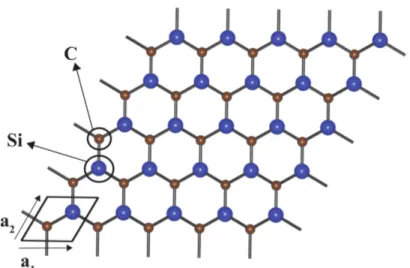
Two Dimensional (2D) SiC
2D honeycomb SiC unit cell can be thought of a graphene unit cell with one carbon atom replaced by a silicon atom. As Si has a larger radius than C, the lattice gets extended. Lattice vectors for honeycomb SiC :
a1 = d( √ 3, 0, 0) a2 = d 2( √ 3, 3, 0) (2.5)
where d ≈ 1.786 ˚A is the Si-C distance. Apparently, it is larger than C-C distance. The reciprocal lattice vectors are given by :
CHAPTER 2. GRAPHENE AND 2D HONEYCOMB SIC 12
Figure 2.4: (Reproduced from Ref.[26]) Graphene nanoribbons terminated by (a) armchair edges and (b) zigzag edges, indicated by filled circles. The unitcells are emphasized by dashed lines. The width “N” of ribbons are defined as the number of carbon atoms in a unit cell.
CHAPTER 2. GRAPHENE AND 2D HONEYCOMB SIC 13
Figure 2.5: Unit cell and lattice vectors of planar honeycomb SiC
b1 = 2π d ( 1 √ 3, − 1 3, 0) b2 = 2π 3d(0, 2, 0) (2.6)
There is no ambiguity in using different lattice vectors from generally used ones for graphene. They are rotationally translated forms of each other and yield the same lattice. General 2D honeycomb SiC plane and its lattice vectors are delineated in Fig. 2.5.
Bare armchair SiC nanoribbons have the similar pattern with those of graphene but have reconstruction at the edges. Upon hydrogen passivation recon-struction vanishes. Zigzag SiC nanoribbons are studied theoretically in a recent paper [41]. Therefore, we did not include them in our study.
Experimental studies of exfoliation and synthesis of single layer SiC do not have the same hasty pace as graphene. In fact, to the best of our knowledge the monolayer SiC has not been obtained up to now. Experimental research has been on honeycomb SiC patches of certain thicknesses.
CHAPTER 2. GRAPHENE AND 2D HONEYCOMB SIC 14
Figure 2.6: (Reproduced from Ref.[44]) Scanning electron microscopy micro-graphs of a short SiC ribbon growing from the tip of a SiC whisker (a) and a SiC whisker growing from the edge of a SiC ribbon (b).
Carbon-rich SiC nanoribbons were fabricated using a nanosecond pulsed laser direct-write and doping (LDWD) technique [42]. The LDWD technique permits synthesis of heterostructured nanoribbons in a single step without additional ma-terial or catalyst, and effectively eliminates the need for nanostructure handling and transferring processes. The resulting nanoribbons comprise three layers each being approximately 50-60 nm thick, containing 15-17 individual sheets.
SiC ribbons were also synthesized by a carbothermal process [44]. the width of the ribbons produced are between 500 nm and 5 µm. The ribbon thicknesses ranged from 50 to 500 nm. Fig. 2.6 and Fig. 2.7 are about the process and the resulting structure .
CHAPTER 2. GRAPHENE AND 2D HONEYCOMB SIC 15
Figure 2.7: (Reproduced from Ref. [44]) Optical micrograph of a SiC ribbon attached to a flat substrate.
Chapter 3
Theoretical Background
3.1
Density Functional Theory
The initial work on DFT was reported in two publications: first by Hohenberg-Kohn in 1964 [47], and the next by Hohenberg-Kohn-Sham in 1965 [48]. This was almost 40 years after Schrodinger (1926) had published his pioneering paper marking the beginning of wave mechanics. Shortly after Schrodinger‘s equation for electronic wave function, Dirac declared that chemistry had come to an end since all its content was entirely contained in that powerful equation. Unfortunately in al-most all cases except for the simple systems like He or H, this equation was too complex to allow a solution. DFT is an alternative approach to the theory of electronic structure, in which the electron density distribution ρ(r) rather than many-electron wave function plays a central role. In the spirit of Thomas-Fermi theory [45, 46], it is suggested that a knowledge of the ground state density of
ρ(r) for any electronic system uniquely determines the system.
3.1.1
Hohenberg-Kohn Formulation
The Hohenberg-Kohn [47] formulation of DFT can be explained by two theorems:
CHAPTER 3. THEORETICAL BACKGROUND 17
Theorem 1: The total energy of the system is univocally determined by the electronic density, except for a trivial additive constant.
Since ρ(r) determines V (r), then it also determines the ground state wave function and gives us the full Hamiltonian for the electronic system. Hence ρ(r) determines implicitly all properties derivable from the hamiltonian H through the solution of the time-dependent Schrodinger equation.
Theorem 2: (Variational Principle) The minimal principle can be formulated in terms trial charge densities, instead of trial wavefunctions.
The ground state energy E could be obtained by solving the Schr¨odinger equation directly or from the Rayleigh-Ritz minimal principle:
E = min{hΨ|H|e Ψie
hΨ|e Ψie }. (3.1) Using ρ(r) instead ofe Ψ(r) was first presented in Hohenberg and Kohn. For ae non-degenerate ground state, the minimum is attained when ρ(r) is the grounde
state density. And energy is given by the equation:
EV[ρ] = F [e ρ] +e Z e ρ(r)V (r)dr, (3.2) with F [ρ] = hΨ[e ρ]|e T +b U|Ψ[b ρ]i,e (3.3) and F [ρ] requires no explicit knowledge of V(r).e
These two theorems form the basis of the DFT. The main remaining error is due to inadequate representation of kinetic energy and it will be cured by the Kohn-Sham equations.
3.1.2
Kohn-Sham Equations
There is a problem with the expression of the kinetic energy in terms of the electronic density. The only expression used until now is the one proposed by
CHAPTER 3. THEORETICAL BACKGROUND 18
Thomas-Fermi, which is local in the density so it does not reflect the short-ranged, non-local character of kinetic energy operator. In 1965, W. Kohn and L. Sham [48] proposed the idea of replacing the kinetic energy of the interacting electrons with that of an equivalent non-interacting system. With this assumption density can be written in atomic units as
ρ(r) = 2 X s=1 Ns X i=1 |ϕi,s(r)|2, (3.4) T [ρ] = 2 X s=1 Ns X i=1 hϕi,s| − ∇2 2 |ϕi,si, (3.5) where ϕi,s‘s are the single particle orbitals which are also the lowest order
eigen-functions of Hamiltonian non-interacting system
{−∇
2
2 + v(r)}ϕi,s(r) = ²i,sϕi,s(r). (3.6) Using new form T [ρ] density functional takes the form
F [ρ] = T [ρ] + 1 2 Z Z ρ(r)ρ(r0) |r − r0| drdr 0 + E XC[ρ], (3.7)
where this equation defines the exchange and correlation energy as a functional of the density. Using this functional in Eq. 3.2, we finally obtain the total energy functional which is known as Kohn-Sham functional [48]
EKS[ρ] = T [ρ] + Z ρ(r)v(r)dr + 1 2 Z Z ρ(r)ρ(r0) |r − r0| drdr 0+ E XC[ρ]. (3.8)
In this way we have expressed the density functional in terms KS orbitals which minimize the kinetic energy under the fixed density constraint. In princi-ple these orbitals are a mathematical object constructed in order to render the problem more tractable, and do not have a sense by themselves. The solution of KS equations has to be obtained by an iterative procedure, in the same way of Hartree and Hartree-Fock equations.
CHAPTER 3. THEORETICAL BACKGROUND 19
3.2
Exchange and Correlation
3.2.1
Local Density Approximation (LDA)
The local density approximation [49] has been the most widely used approxima-tion to handle exchange-correlaapproxima-tion energy. Its philosophy was already present in Thomas-Fermi theory. The main idea of LDA is to consider the general inhomo-geneous electronic systems as locally homoinhomo-geneous and then use the exchange-correlation corresponding to that of the homogeneous electron gas.
LDA favors more homogeneous systems. It over-binds molecules and solids but the chemical trends are usually correct.
3.2.2
Generalized Gradient Approximation (GGA)
Once the extent of the approximations involved in the LDA has been understood, one can start constructing better approximations. The most popular approach is to introduce semi-locally the inhomogeneties of the density, by expanding EXC[ρ]
as a series in terms of the density and its gradients. This approximation is known as GGA [50] and its basic idea is to express the exchange-correlation energy in the following form:
EXC[ρ] =
Z
ρ(r)²XC[ρ(r)]dr +
Z
FXC[ρ(r, ∇ρ(r))]dr (3.9)
where the functional FXC is asked to satisfy the formal conditions.
GGA approximation improves binding energies, atomic energies, bond lengths and bond angles when compared the ones obtained by LDA.
3.3
Periodic Supercells
By using the represented formalisms observables of many-body systems can be transformed into single particle equivalents. However, there still remains two
CHAPTER 3. THEORETICAL BACKGROUND 20
difficulties: A wave function must be calculated for each of the electrons in the system and the basis set required to expand each wave function is infinite since they extend over the entire solid. For periodic systems both problems can be handled by Bloch‘s theorem [51].
3.3.1
Bloch‘s Theorem
Bloch theorem states that in a solid having translational periodicity each elec-tronic wave function can be written as:
Ψi(r) = ui(r)eikr, (3.10)
where uk has the period of crystal lattice with uk(r) = uk(r+T). This part can
be expanded using a basis set consisting of reciprocal lattice vectors of the crystal.
ui(r) =
X
G
ak,Gei(G)r. (3.11)
Therefore each electronic wave function can be written as a sum of plane waves Ψi(r) =
X
G
ai,k+Gei(k+G)r. (3.12)
3.3.2
k-point Sampling
Electronic states are only allowed at a set of k-points determined by boundary conditions. The density of allowed k-points are proportional to the volume of the cell. The occupied states at each k-point contribute to the electronic potential in the bulk solid, so that in principle, an infinite number of calculations are needed to compute this potential. However, the electronic wave functions at k-points that are very close to each other, will be almost identical. Hence, a single k-point will be sufficient to represent the wave functions over a particular region of k-space. There are several methods which calculate the electronic states at special k points in the Brillouin zone [52]. Using these methods one can obtain an accurate approximation for the electronic potential and total energy at a small number of k-points. The magnitude of any error can be reduced by using a denser set of k-points.
CHAPTER 3. THEORETICAL BACKGROUND 21
3.3.3
Plane-wave Basis Sets
According to Bloch‘s theorem, the electronic wave functions at each k-point can be extended in terms of a discrete wave basis set. Infinite number of plane-waves are needed to perform such expansion. However, the coefficients for the plane waves with small kinetic energy (¯h2/2m)|k + G|2 are more important than
those with large kinetic energy. Thus some particular cutoff energy can be de-termined to include finite number of k-points. The truncation of the plane-wave basis set at a finite cutoff energy will lead to an error in computed energy. How-ever, by increasing the cutoff energy the magnitude of the error can be reduced.
3.3.4
Plane-wave Representation of Kohn-Sham
Equa-tions
When plane waves are used as a basis set, the Kohn-Sham (KS) [48] equations assume a particularly simple form. In this form, the kinetic energy is diagonal and potentials are described in terms of their Fourier transforms. Solution proceeds by diagonalization of the Hamiltonian matrix. The size of the matrix is determined by the choice of cutoff energy, and will be very large for systems that contain both valence and core electrons. This is a severe problem, but it can be overcome by considering pseudopotential approximation.
3.3.5
Nonperiodic Systems
The Bloch Theorem cannot be applied to a non-periodic systems, such as a system with a single defect. A continuous plane-wave basis set would be required to solve such systems. Calculations using plane-wave basis sets can only be performed on these systems if a periodic supercell is used. Periodic boundary conditions are applied to supercell so that the supercell is reproduced through out the space. As seen schematically in Fig. 3.1 even molecules can be studied by constructing a large enough supercell which prevents interactions between molecules.
CHAPTER 3. THEORETICAL BACKGROUND 22
Figure 3.1: (Reproduced from Ref.[43])Supercell geometry for a molecule. Super-cell is chosen large enough to prevent interactions the molecules.
3.4
Pseudopotential Approximation
The act of using a pseudopotential constitutes for replacing the Coulomb potential of the necleus and the inner core electrons by an effective potential on valence electrons. Once the pseudopotential is generated by an atomic calculation, it can be used to compute material characteristics of an atom in a molecule.
In plane wave calculations, valence wave functions are expanded in Fourier series. The more Fourier components are used the more the computational cost increases. The term “smoothness” means minimizing the range in Fourier space, which is needed to describe the valence properties to a given accuracy. Fig. 3.2 gives a comparison between all-electron and pseudopotential approaches.
CHAPTER 3. THEORETICAL BACKGROUND 23
Figure 3.2: (Reproduced from Ref.[43])Illustration of all-electron (solid lines) and pseudoelectron (dashed lines) potentials and their corresponding wave functions.
3.4.1
Projector Augmented Waves (PAWs)
The projector augmented wave (PAW) method is a reformulation of the OPW (Orthogonolized Plane Wave) method with an adaptation to modern techniques for calculation of total energy, forces etc. It comprises projectors and auxiliary localized functions. The difference with the ultrasoft pseudopotential is that PAW keeps the full all-electron wave function. Due to rapid oscillation of the full wave function around the nucleus, all integrals are evaluated as a combination of integrals of smooth functions.
Main ideas of PAW can be sketched as follows:
Let |ψeυ
ii be smooth part of valence and |ψυii be all electron valence
wave-function. (omit superscript υ from now on) The unitary transformation between them is |ψii = τ |ψeii .
CHAPTER 3. THEORETICAL BACKGROUND 24
|ψeii =
X
m
cm|ψemi (3.13)
The transformation to all electron function :
|ψii = τ |ψeii =
X
m
cm|ψmi (3.14)
Full wavefunction in all space :
|ψi = |ψi +e X
m
cm{|ψmi − |ψemi} (3.15)
τ is linear. The coefficients are :
cm = hpem|ψie (3.16)
with pem being a projection operator.
Transformation operator becomes:
τ = 1 +X
m
{|ψmi − |ψemi} (3.17)
Any operator A can be transformed toA for smooth part of wavefunctions ase
:
e
A = τ†Aτ = A + X mm0
|pemi{hψm|A|ψm0i − hψem|A|ψem0i}hpm0| (3.18)
Expressions for physical quantities can be derived using Eqs. (3.17) and (3.18) .
PAW method can provide the core wavefunctions. From these core wavefunc-tions, full wavefunctions can be developed [53].
CHAPTER 3. THEORETICAL BACKGROUND 25
3.5
Phonon Calculations
3.5.1
Phonon frequencies
The central quantity in the calculation of the phonon frequencies is the force-constant matrix Φisα,jtβ, since the frequencies at wavevector k are the eigenvalues
of the dynamical matrix Dsα,tβ, defined as:
Dsα,tβ(k) = 1 √ MsMt X i Φisα,jtβexp(ik(R0j + τt− R0i − τs), (3.19) where R0
i is a vector of the lattice connecting different primitive cells and
τs is the position of the atom s in the primitive cell. If we have the complete
force-constant matrix, then Dsα,tβ and hence the frequencies ωks can be obtained
at any k. In principle, the elements of Φisα,jtβ are non-zero for arbitrarily large
separations | R0
j+τt−R0i−τs |, but in practice they decay rapidly with separation,
so that a key issue in achieving our target precision is the cut-off distance beyond which the elements can be neglected.
3.5.2
Calculation of the force constant matrix
We calculate Φisα,jtβ by the small-displacement method. In harmonic
approxi-mation the α Cartesian component of the force exerted on the atom at position R0 i + τs is Fisα = − X jtβ Φisα,jtβujtβ (3.20)
where ujsβ is the displacement of the atom in R0j + τt along the direction β.
CHAPTER 3. THEORETICAL BACKGROUND 26
Φisα,jtβ = −
Fisα,jtβ
ujtβ
(3.21)
by displacing once at a time all the atoms of the lattice along the three Carte-sian components by ujtβ, and calculating the forces Fisα,jtβ induced on the atoms
in R0
i + τs. Since the crystal is invariant under translations of any lattice vector,
it is only necessary to displace the atoms in one primitive cell and calculate the forces induced on all the other atoms of the crystal. In what follows we will assume this as understood and put simply j = 0.
It is important to appreciate that the Φlsα,l0tβin the formula for Dsα,tβ(k) is the
force-constant matrix in the infinite lattice, with no restriction on the wavevector k, whereas the calculations of Φlsα,l0tβ can only be done in supercell geometry.
Without a further assumption, it is strictly impossible to extract the infinite-lattice Φlsα,l0tβ from supercell calculations, since the latter deliver information
only at wavevectors that are reciprocal lattice vectors of the superlattice . The further assumption needed is that the infinite-lattice Φlsα,l0tβ vanishes when the
separation Rl0t−Rlsis such that the positions Rlsand Rl0tlie in different
Wigner-Seitz (WS) cells of the chosen superlattice. More precisely, if we take the WS cell centred on Rl0t, then the infinite-lattice value of Φlsα,l0tβ vanishes if Rls is in
a different WS cell; it is equal to the supercell value if Rls is wholly within the
same WS cell; and it is equal to the supercell value divided by an integer P if Rls lies on the boundary of the same WS cell, where P is the number of WS cells
having Rls on their boundary. With this assumption, the Φlsα,l0tβ elements will
converge to the correct infinite-lattice values as the dimensions of the supercell are systematically increased.
It is not always necessary to displace all the atoms in the primitive cell, since the use of symmetries can reduce the amount of work needed. This is done as follows. We displace one atom in the primitive cell, let’s call it ’one’, and we calculate the forces induced by the displacement on all the other atoms of the supercell. Then we pick up one other atom of the primitive cell, atom ’two’. If there is a symmetry operation S (not necessarily a point group symmetry operation) such that, when S is applied to the crystal atom two is sent into
CHAPTER 3. THEORETICAL BACKGROUND 27
atom one and the whole crystal is invariant under such transformation, then it is not necessary to displace atom two, and the part of the force constant matrix associated with its displacement can be calculated using :
Φis,02 = B(S)Φλis(S),01B(S
−1) (3.22)
where B(S) is the 3 × 3 matrix representing the point group part of S in Cartesian coordinates, and λis(S) indicates the atom of the crystal where the
atom in R0
i + τs is brought because of the action of the symmetry operation S.
If there is no symmetry operation connecting atom two to atom one then atom two is displaced and all the induced force field is calculated. The procedure is repeated for all the atoms of the primitive cell.
In principle each atom has to be displaced along the three Cartesian directions. It is sometimes convenient to displace the atoms along some special directions so as to maximize the number of symmetry operations still present in the ’excited’ supercell, in this way the calculations of the forces are less expensive. This can al-ways be done, as long as one displaces the atoms along three linearly independent directions. The forces induced by the displacements along the three Cartesian directions is easily reconstructed by the linear combination :
Fis,0tα =
X
l
AlαF˜is,0tk (3.23)
where ˜Fis,0tk is the force induced on the atom in R0i+ τs due to a displacement
of the atom in τt along the direction uk, and A = (|uu11|,|uu22|,|uu33|)−1is the inverse
of the 3 × 3 matrix whose columns are the normalized displacements in Cartesian coordinates.
Using symmetries it is possible to reduce the number of displacements even further: if applying a point group symmetry operation U to the displacement vector u1 one obtains a vector u2 which is linearly independent from u1, then the
CHAPTER 3. THEORETICAL BACKGROUND 28
Fis,0t2 = B(U)Fλis(U−1),0t1. (3.24)
a linearly independent direction cannot be found one has to displace the atom along a chosen independent direction and perform an other calculation. This is done until a set of three independent directions is found.
The force constant matrix is invariant under the point group symmetry oper-ations of the crystal. This is not automatically guaranteed by the procedure just described, because in general the crystal is not harmonic. So, the force constant matrix must be symmetrized with respect to the point group operations of the crystal: Φis,0t= 1 NG X U B(U)Φλis(U ),0tB(U −1). (3.25)
The symmetrization of the force constant matrix removes all even-order an-harmonicities. The harmonic approximation becomes better and better as the displacement are made smaller and smaller. However, if the displacements are small, also the force induced are small, but there is a limit in the accuracy achiev-able in the calculations, so one cannot make too small displacements [55].
Chapter 4
Results
4.1
Introduction
Synthesis of a single atomic plane of graphite, i.e. graphene with covalently bonded honeycomb lattice has been a breakthrough for several reasons [23, 56, 57]. Firstly, electrons behaving as if massless Dirac fermions have made the observa-tion of several relativistic effects possible. Secondly, stable graphene has disproved previous theories, which were concluded that two-dimensional structures cannot be stable. Graphene displaying exceptional properties, such as high mobility even at room temperature, ambipolar effect, Klein tunnelling, anomalous quantum hall effect etc. seems to offer novel applications in various fields [58]. Not only 2D graphene, but also its quasi 1D forms, such as armchair and zigzag nanoribbons have shown novel electronic and magnetic properties [59, 60, 61], which can lead to important applications in nanotechnology. As a result, 2D honeycomb struc-tures derived from Group IV elements and Group III-V and II-VI compounds are currently generating significant interest owing to their unique properties.
Boron nitride (BN) in ionic honeycomb lattice which is the Group III-V ana-logue of graphene has also been produced having desired insulator characteris-tics [62]. Nanosheets [63, 64], nanocones [65], nanotubes [66], nanohorns [67], nanorods [68] and nanowires [69] of BN have already been synthesized and these
CHAPTER 4. RESULTS 30
systems might hold promise for novel technological applications. Among all these different structures, BN nanoribbons, where the charge carriers are confined in two dimension and free to move in third direction, are particularly important due to their well defined geometry and possible ease of manipulation.
BN nanoribbons posses different electronic and magnetic properties depending on their size and edge termination. Recently, the variation of band gaps of BN nanoribbons with their widths and Stark effect due to applied electric field have been studied [70, 71]. The magnetic properties of zigzag BN nanoribbons have been investigated [72]. Half-metallic properties have been revealed from these studies which might be important for spintronic applications. Production of graphene nanoribbons as small as 10 nm in width has been achieved [73, 74] and similar techniques are expected to be developed for BN nanoribbons.
Another example of graphene-like structures is monolayer honeycomb zinc ox-ide (ZnO). The monolayer of ZnO is a III-V ionic compound and has the honey-comb structure similar to graphene and BN. Very thin nanosheets [75], nanobelts [76], nanotubes [77] and nanowires [78] of ZnO have already been synthesized. Two monolayer thick ZnO(0001) films grown on Ag(111) were reported [79].
Quasi one dimensional (1D) ZnO nanoribbons show diverse electronic and magnetic properties depending on their size and edge termination. Recently, it has been predicted that the ferromagnetic behavior of ZnO nanoribbons due to unpaired spins at the edges is dominated by oxygen atoms [80, 81]. Apparently, 2D and 1D honeycomb structure of ZnO can provide us with exceptional elec-tronic and magnetic properties and hence hold the promise of novel technological applications.
In a recent paper, a comprehensive analysis of the atomic, electronic and magnetic properties of monolayer, bilayer and nanoribbons of ZnO are carried out using first-principles calculations. Having presented the analysis on the stability of 2D and 1D ZnO in honeycomb structures, electronic and magnetic properties of single and bilayer ZnO in honeycomb structures were investigated. They are nonmagnetic semiconductors, but attain magnetic properties upon creation of Zn-vacancy defect. ZnO nanoribbons exhibit interesting electronic and magnetic
CHAPTER 4. RESULTS 31
properties depending on their orientation. While armchair ZnO nanoribbons are nonmagnetic semiconductors with band gaps varying with their widths, bare zigzag nanoribbons are ferromagnetic metals. These electronic and magnetic properties show dramatic changes under elastic and plastic deformation. Hence, ZnO nanoribbons can be functionalized by plastic deformation [82].
Earlier, planar honeycomb structure of carbon was exfoliated and its physical properties were analyzed [23, 56, 57]. The honeycomb structure is common to 2D single layer of SiC and graphene. However, despite graphene being strictly pla-nar, honeycomb structure of Si is unstable, but it is stabilized by puckering. The puckered honeycomb structure of Si is referred to as silicene [27]. The first theo-retical study of single layer honeycomb SiC and its selected zigzag and armchair nanoribbons are presented recently [41].
In this thesis, a comprehensive analysis of the atomic, electronic and magnetic properties of 2D monolayer of SiC honeycomb structure and its bare and hydrogen passivated armchair nanoribbons (A-SiCNR) are carried out using first-principles calculations. We started with the discussion of 3D zincblende and wurtzite crys-tals, as well as SiC atomic chain as an ultimate 1D system; we presented an analysis of optimized atomic structures with corresponding phonon dispersion curves and electronic energy band structures and effective charges. Then we pro-vided an extensive analysis of single layer 2D and quasi-1D (nanoribbon) SiC in terms of optimized atomic structures and their stability, electronic and magnetic structures. We revealed elastic constants, such as in-plane stiffness and Poisson’s ratio using our method developed for honeycomb structures. Having made the results for 1D, 2D and 3D structures, we presented a comprehensive discussion of dimensionality effects. Then we investigated the effect of vacancy defects (such as Si and C vacancy, SiC vacancy and C+Si antisite defect) on the electronic and magnetic properties of monolayer SiC and its armchair nanoribbons. Further-more, we showed that SiC can be functionalized through adsorption of a foreign atom to the surface of 2D SiC or through substitution of either C or Si with a foreign atom. We found that 2D SiC and its ribbons provide new physical prop-erties, which extend those of 3D SiC crystals for technological applications. For example, while various allotropic forms of SiC including its honeycomb structures
CHAPTER 4. RESULTS 32
are normally nonmagnetic semiconductors, a Si vacancy gives rise to spin polar-ization. Significant variation of the band gap of narrow A-SiCNRs may be crucial in optoelectronic nanodevices.
4.2
Method of calculations
We have performed first-principles plane wave calculations within Density Func-tional Theory (DFT) using PAW potentials [83]. The exchange correlation poten-tial has been approximated by Generalized Gradient Approximation (GGA) using PW91 [84] functional both for spin-polarized and spin-unpolarized cases. For the sake of comparison calculations are also carried out using different potentials and exchange-correlation approximations. All structures have been treated within su-percell geometry using the periodic boundary conditions. A plane-wave basis set with kinetic energy cutoff of 500 eV has been used. The interaction between SiC monolayers in adjacent supercells is hindered by a minimum 12 ˚A vacuum spac-ing. In the self-consistent potential and total energy calculations, when finding the optimum lattice constants the Brillouin zone (BZ) is sampled by, respectively (5×5×5), (11×11×1) and (11×1×1) special k-points for 3D bulk, 2D honey-comb and 1D nanoribbons of SiC. Further relaxation is made with (11×11×11), (31×31×1) and (25×1×1) special k-points in order to find the ultimate structure and charge density. All atomic positions and lattice constants are optimized by using the conjugate gradient method, where the total energy and atomic forces are minimized. Pressure on the cell was minimized automatically during this pro-cess. The convergence for energy is chosen as 10−5 eV between two steps and the
maximum Hellmann-Feynman forces acting on each atom is less than 0.04 eV/˚A upon ionic relaxation. The pseudopotentials corresponding to 4 valence electrons of Si (Si:3s2 3p2) and C (C:2s2 2p2) are used. Numerical plane wave calculations
are performed by using VASP [85, 86]. Part of the calculations have also been repeated by using SIESTA [88] software. The cohesive energy of any structure SiC is found as EC = ET[SiC] − ET[Si] − ET[C] in terms of the optimized total
energy of any SiC structure,and the total energies of free Si and C atoms, all calculated in the same supercell using the same parameters. Phonon calculations
CHAPTER 4. RESULTS 33
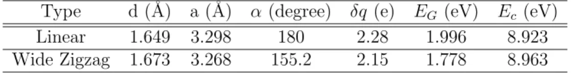
Table 4.1: Si-C bond length (d), lattice constant (a), kink angle (α ), bandgap (EG), cohesive energy (Ec) values for two different types of SiC chains
Type d (˚A) a (˚A) α (degree) δq (e) EG (eV) Ec (eV)
Linear 1.649 3.298 180 2.28 1.996 8.923 Wide Zigzag 1.673 3.268 155.2 2.15 1.778 8.963
were carried out using PHON program [87] implementing force constant method.
4.3
1D atomic chain and 3D bulk crystal of SiC
In this section, we present a brief discussion of 1D SiC atomic chain and 3D bulk crystal based on our structure optimized total energy, phonon and electronic energy calculations. Studies [3, 2] on SiC bulk lattice and atomic chains [89] already exist in the literature. However, our purpose is, however to carry out calculations with same parameters as used in 2D single layer SiC honeycomb structure and provide a consistent comparison of dimensionality effects.
4.3.1
1D SiC Chains
Earlier, the first theoretical study of Group IV and III-V binary compounds were reported by Durgun et. al [89]. They examined SiC atomic chain as a function of lattice parameter and found that the wide zigzag atomic chain of SiC with bond angle of ∼147◦ is energetically more favorable than the linear and narrow
angle zigzag chains. Present calculations find that the atomic chains of SiC are nonmagnetic. Calculated structural parameters, cohesive energies, band gap and phonon modes of linear and zigzag atomic chains, which are relevant for the present study are given in Fig. 4.1. The lattice constant of the linear SiC chain,
a = 3.298 ˚A, Si-C bond distance, d = 1.649 ˚A. The charge transfer from Si to C is δq= 2.28 electrons, calculated by using Bader analysis [90]. Important characteristics of SiC chains are summarised in Table 4.1.
CHAPTER 4. RESULTS 34
Phonon modes calculated with force constant method have imaginary frequen-cies : two acoustical and two optical branches of linear SiC chain have imaginary frequencies. Wide angle zigzag SiC chain has one optical and one acoustical branches with imaginary frequencies. These results indicate that free standing SiC chains are unstable.
4.3.2
3D SiC Crystals
Our work on bulk SiC includes wurtzite (wz) and zincblende (zb) structures. Atoms in wz- and zb-SiC are four fold coordinated through tetrahedrally di-rected sp3-orbitals. Calculated structural parameters, cohesive energies(eV),
en-ergy band structures and phonon modes are given in Fig. 4.2. Zincblende SiC structure in Tdsymmetry has cubic lattice constants are a1 = a2 = a3 = 3.096 ˚A.
Si-C bond distance(d) is 1.896 ˚A. There are four tetrahedrally coordinated bonds from each atom, all of which are equal. Charge transfer from Si to C is δq= 2.59 electrons calculated via Bader analysis [90]. While the GGA band gap is 1.406 eV, it increases to 2.4 eV after GW0 [91] correction is taken into account. As
for wz-SiC crystal, the hexagonal lattice constants of the optimized structure in equilibrium are a1 = a2 = 3.093 ˚A, c/a = 1.63307. The deviation of c/a from the
ideal value of 1.633 imposes a slight anisotropy on the lengths of tetrahedrally directed Si-C bonds. While the length of three short bonds is 1.892 ˚A, the fourth bond is slightly longer and has the length of 1.9 ˚A. Charge transfer from Si to C is δq= 2.63 electrons. The GGA band gap is 2.316 eV, but it increases to 3.32 eV after GW0 correction. Corrected badgaps are exactly the same as those
from the experiment [92].The calculated structural parameters and energy band gaps are in reasonable agrement with the earlier calculations and experimental measurements.
Five out of six phonon modes of SiC zincblende are in complete agreement with literature [93]. The highest optical mode goes down and couples with nearest optical mode. The same problem is present in the wurtzite SiC. Again other five phonon modes of wurtzite structure agrees with literature [94].
CHAPTER 4. RESULTS 35
Figure 4.1: Atomic structures, electronic energy bands and dispersion of phonon modes of linear and zigzag SiC atomic chains. Ec and EG are cohesive and band
gap energies, respectively. Si and C atoms are shown by blue-large and black small balls, respectively.
CHAPTER 4. RESULTS 36
Figure 4.2: Optimized atomic structure with relevant structural parameters, cor-responding energy band structure and frequencies of phonon modes of 3D bulk SiC in zincblende and wurtzite structures. Zero of energy of the band structure is set at the Fermi level, and band gap is shaded.
CHAPTER 4. RESULTS 37
Table 4.2: Si-C bond length(d), lattice constant (a), bandgap (EG), cohesive
energy (Ec) values for the monolayer SiC calculated with different potentials
Potential d (˚A) a (˚A) EG (eV) Ec (eV)
PAW + GGA 1.786 3.094 2.53 11.94 PAW + LDA 1.77 3.07 2.51 13.54 US + GGA 1.776 3.079 2.542 11.97 US + LDA 1.759 3.048 2.532 13.47
4.4
2D Honeycomb SiC
Two-dimensional hexagonal structure of SiC is optimized using periodically re-peating supercell having 15 ˚A spacing between SiC planes. The minimum of total energy occurred when Si and C atoms are placed in the same plane forming a honeycomb structure. The magnitude of the Bravais vectors of the hexagonal lattice is found to be a1 = a2= 3.094 ˚A (see Fig. 4.3), and the Si-C bond to
be d =1.786 ˚A. The planar structure of 2D SiC is tested by displacing Si and C atoms arbitrarily from their equilibrium positions and then reoptimizing the structure. Upon optimization, the displaced atoms returned to their original po-sitions in the same plane. 2D honeycomb SiC is found to be a semiconductor with a GGA band gap of 2.53 eV using LDA as well as GGA. Furthermore, in Table 4.2, we give lattice constant, bond length, cohesive energy, energy gap val-ues of SiC honeycomb structure calculated with different parameters. Since DFT usually underestimates the band gap of semiconductors, we corrected the GGA band gap using GW0 correction and found it to be 3.90 eV. The charge transfer
from Si to C in 2D honeycomb SiC is calculated to be δq= 2.53 eV electrons. Earlier DFT calculations [41] on 2D honeycomb SiC and its ribbons used PAW [83] potentials and GGA approximation via VASP [85, 86]. Their results are in reasonable agreement with ours.
Our phonon modes were calculated with force constant method [87] . Since all the modes are positive, a single layer SiC sheet is stable. Forces were found by displacing a single atom in a 7×7×1 supercell by 0.4 ˚A. We use a small displace-ment in order to stay in the harmonic region. We increased default grids used
CHAPTER 4. RESULTS 38
Figure 4.3: Optimized atomic structure, energy band structure and phonon modes of 2D SiC in honeycomb structure. The primitive unit cell is delineated. The zero of energy in the band structure is set to the Fermi level.
by VASP until calculations converge to a sensible result . Since problem arises due to the lowest acoustic mode which presents an out of plane displacement. A fictitious dip near Γ point occurs in crude calculations, but it can be overcome by refining the mesh in the z- axis (perpendicular to plane) as much as possible. By this way, force in that direction is calculated more rigorously.
4.4.1
Dimensionality effects
In Table 4.3, we compare the variation of the effective charge on Si and C atoms, namely Z∗
CHAPTER 4. RESULTS 39
Table 4.3: Si-C bonding type, bond length(d), lattice constant (a), charge transfer (δq), bandgap (EG), cohesive energy (Ec) comparison for SiC polymorphs
Material Bonding d (˚A) a (˚A) δq (e) EG (eV) Ec (eV)
Linear Chain sp 1.649 3.298 2.28 1.996 8.923 Wide Zigzag Chain sp 1.673 3.268 2.15 1.778 8.963 2D Honeycomb sp2 1.786 3.094 2.53 2.53 11.94
Zincblende sp3 1.896 3.096 2.59 1.406 12.939
Wurtzite sp3 1.892 (3), 1.9 (1) 3.093 2.63 2.3161 12.932
Si-C bond length d; lattice constant a, cohesive energy per Si-C, Ec; band gap
EG calculated for SiC in different dimensionalities. It should be noted the length
of Si-C bonds of 2D SiC honeycomb structure is smaller than that in the 3D bulk (wz, zb) crystals, but larger than that in zigzag atomic chains. Here we see that the dimensionality effect is reflected to the strength of the bonding through
spn hybridization, where n coincides with the dimensionality. While sp2 hybrid
orbitals of 2D planar honeycomb structure form stronger bonds than tetrahedrally coordinated sp3 orbitals of 3D bulk, they are relatively weaker than sp hybrid
orbitals of 1D chain.
4.5
Bare and Hydrogen Passivated SiC
Nanorib-bons
In this section, we consider bare and hydrogen passivated (H-pass) armchair SiC nanoribbons (A-SiCNR). These nanoribbons are specified according to their width given in terms of N number of Si-C atom pairs in their unit cells. Hence, A-SiCNR(N) indicates armchair SiC nanoribbons having N Si-C pairs in their unit cell. We have analyzed odd numbered A-SiCNR (both bare and H-passivated) from 5 to 21, which have reflection symmetry with respect to their axis. We in-vestigated their atomic structure; electronic, magnetic properties. Bare armchair
![Figure 2.1: (Reproduced from Ref.[26]) Graphene, graphite, single-walled carbon nanotube (SWNT) and C 60 structures make sp 2 type bonding, whereas diamond makes sp 3 type bonding](https://thumb-eu.123doks.com/thumbv2/9libnet/5753004.116165/19.892.210.749.180.486/figure-reproduced-graphene-graphite-nanotube-structures-bonding-diamond.webp)
![Figure 2.2: (Reproduced from Ref.[26]) Left: Lattice structure of graphene made of two interpenetrating hexagonal lattices ( a 1 and a 2 are lattice unit vectors, and δ i , i=1,2,3 are the nearest neighbor vectors); Right: corresponding Brillouin zone](https://thumb-eu.123doks.com/thumbv2/9libnet/5753004.116165/21.892.259.705.195.395/reproduced-lattice-structure-graphene-interpenetrating-hexagonal-corresponding-brillouin.webp)
![Figure 2.3: (Reproduced from Ref.[26]) Band structure of the bare graphene calculated for the 2×2 unitcell.](https://thumb-eu.123doks.com/thumbv2/9libnet/5753004.116165/22.892.286.676.184.468/figure-reproduced-ref-band-structure-graphene-calculated-unitcell.webp)
![Figure 2.4: (Reproduced from Ref.[26]) Graphene nanoribbons terminated by (a) armchair edges and (b) zigzag edges, indicated by filled circles](https://thumb-eu.123doks.com/thumbv2/9libnet/5753004.116165/24.892.195.764.341.771/figure-reproduced-graphene-nanoribbons-terminated-armchair-indicated-circles.webp)
![Figure 2.7: (Reproduced from Ref. [44]) Optical micrograph of a SiC ribbon attached to a flat substrate.](https://thumb-eu.123doks.com/thumbv2/9libnet/5753004.116165/27.892.238.730.487.736/figure-reproduced-ref-optical-micrograph-ribbon-attached-substrate.webp)
![Figure 3.1: (Reproduced from Ref.[43])Supercell geometry for a molecule. Super- Super-cell is chosen large enough to prevent interactions the molecules.](https://thumb-eu.123doks.com/thumbv2/9libnet/5753004.116165/34.892.325.646.194.500/figure-reproduced-supercell-geometry-molecule-prevent-interactions-molecules.webp)
![Figure 3.2: (Reproduced from Ref.[43])Illustration of all-electron (solid lines) and pseudoelectron (dashed lines) potentials and their corresponding wave functions.](https://thumb-eu.123doks.com/thumbv2/9libnet/5753004.116165/35.892.370.597.191.488/figure-reproduced-illustration-electron-pseudoelectron-potentials-corresponding-functions.webp)