See discussions, stats, and author profiles for this publication at: https://www.researchgate.net/publication/299133447
Effect of various pseudomorphic AlN layer insertions on the electron densities of
two-dimensional electron gas in lattice-matched In0.18Al0.82N/GaN based
heterostructures
Article in OPTOELECTRONICS AND ADVANCED MATERIALS-RAPID COMMUNICATIONS · September 2009
CITATIONS
0
READS
24
2 authors, including:
Some of the authors of this publication are also working on these related projects:
Thz spectroscopyView project
lithography-free broadband absorbersView project Ekmel Ozbay
Bilkent University
696PUBLICATIONS 16,774CITATIONS
SEE PROFILE
All content following this page was uploaded by Sefer Bora Lisesivdin on 23 March 2016.
Effect of various pseudomorphic AlN layer insertions on
the electron densities of two-dimensional electron gas in
lattice-matched In
0.18
Al
0.82
N/GaN based heterostructures
S. B. LISESIVDINa*, E. OZBAYa, b
aNanotechnology Research Center, Bilkent University, Bilkent, 06800 Ankara, Turkey
bDepartment of Physics, Bilkent University, Bilkent, 06800 Ankara, Turkey; and Department of Electrical and Electronics Engineering, Bilkent University, Bilkent, 06800 Ankara, Turkey
We explored the effects of various pseudomorphic AlN layer insertions in lattice-matched In0.18Al0.82N/GaN based
heterostructures on band structures and carrier densities with the help of one-dimensional self-consistent solutions of non-linear Schrödinger-Poisson equations. According to the calculations, important increase in carrier density is expected with an increasing number of AlN insertions in In0.18Al0.82N barrier. The effect of the position of an AlN layer in In0.18Al0.82N barrier
is also investigated. An additional AlN layer insertion in the GaN layer is calculated in detail with the help of an experimental point of view, in which the possible effects on both carrier density and mobility are discussed.
(Received September 09, 2009; accepted September 15, 2009)
Keywords: AlInN, InAlN, HEMT, Schrödinger, Poisson, 2DEG, Heterostructure
1. Introduction
GaN-based field effect transistors have attracted much attention for high–power, –frequency and –temperature applications [1] since the pioneering study of Khan et al.[2]. These transistors primarily consist of a tensely strained AlGaN layer that is grown on a GaN layer. The strain between the layers induces a piezoelectric polarization field, in which all the layers have additional pyroelectric polarization fields (spontaneous polarization). These polarization fields lead to the formation of a high mobility two-dimensional electron gas (2DEG) at the interface with sheet carrier densities at an order of
~1.0×1013 cm-2. In order to increase mobility and carrier
density, two important improvements helped to change the overall system that Khan originally proposed. The first one was proposed by Smorchkova et al. where a thin (~1-2 nm) AlN interlayer was inserted between the AlGaN and GaN layers [3]. This interlayer reduces the alloy scattering of electrons in turn resulting in increased mobility [4-6]. Due to the additional strain that the interlayer introduces, the carrier density is also increased. The latter one is to increase the Al content of the AlGaN barrier layer. A high Al content in the AlGaN barrier layer improves the polarization induced carrier density and carrier confinement [7]. However, due to high strain that is induced by the high Al content, strain relaxations that create a significant drop in mobility and carrier density may occur [8].
In 2001, Kuzmik proposed a nearly lattice-matched
InxAl1-xN/GaN structure (x~0.18) to increase the carrier
density [9]. In nearly lattice-matched InxAl1-xN/GaN
structures, piezoelectric polarization is negligible and all
the carriers are supplied by spontaneous polarization only. Because of high spontaneous polarization that is provided by large spontaneous polarization difference between InAlN and GaN layers, these structures show sheet carrier
densities of
3
−
3
.
5
×
10
13 cm-2 [10, 11]. With highercarrier densities, the high performance HEMT structures with a cutoff frequency of 26 GHz (with a maximum power gain cutoff frequency of 40 GHz) and 2 A/mm drain-source current-densities are already measured [12]. Just as in AlGaN/GaN counterparts, with a thin AlN layer insertion between the InAlN and GaN layers, any possible material diffusion between these layers are prevented as much as possible. Moreover, with the increased conduction band offset between the layers, alloy scattering becomes negligible and high mobilities can be obtained. In addition, carrier density can also be increased due to piezoelectric polarization that is induced by the interlayer. AlN interlayer insertion in InAlN/GaN structures has been studied recently by several groups [11, 13] with respect to AlN thicknesses. In order to design high-quality, low density structures, knowledge of strain and the investigation of AlN insertions below strain relaxation
limits are essential. Because of In0.18Al0.82N and GaN
materials are nearly lattice-matched, strain calculations for a GaN/AlN/GaN semiconductor-insulator-semiconductor (SIS) structure can also be acceptable for
In0.18Al0.82N/GaN structures [14].
In the present paper, we theoretically explore the various pseudomorphic AlN layer insertions on the
In0.18Al0.82N barrier, in the In0.18Al0.82N barrier, and in the
GaN layer of a lattice-matched In0.18Al0.82N/GaN structure,
respectively. The effects of insertions on band structures and carrier densities were investigated by solving
non-Effect of various pseudomorphic AlN layer insertions on the electron densities of two-dimensional electron gas … 905
linear Schrödinger-Poisson equations, self-consistently including polarization induced carriers [15]. All of the investigations are below the calculated elastic strain relaxation limits [14].
2. Simulation
The simulation procedure begins with a strain calculation with homogeneous strain dispersion over the simulated region. The strain in a GaN-based material produces a piezoelectric polarization that directly affects the electronic and optical properties of the material. The band edges are calculated by taking full account of the van-de-Walle model and strain. With the calculated strain, the piezoelectric charges are then calculated. The quantum states are allocated in previously determined quantum regions. After that, a starting potential value is determined and the nonlinear Poisson equation is solved with the calculated piezoelectric and spontaneous charges. In the last step of the simulation, Schrödinger’s equation and Poisson’s equation are solved self-consistently in order to obtain the carrier distribution, wave functions, and related eigenenergies. The material parameters of AlN, GaN, and InN, which are used by the simulator, are taken from
several references [16-19] and the InxAl1-xN parameters
are extrapolated with Vegard’s law.
The conduction band structures and electron densities are found for different AlN insertion investigations. In every case, the strain values are found to be below the strain relaxation limit for the related structure. A simple estimation for the critical thickness below the strain
relaxation limit is given by the relation [11] :
t
cr≅
b
eε
xx.Here, be is the Burger's vector with a value of be=0.31825
nm [20] and εxx is the in-plain strain value for the wurtzite
material. We assume a total homogeneous strain over the GaN layer, which includes the strain values of every layer over the GaN layer.
3. Results and discussion
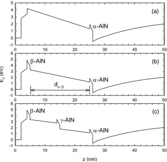
Fig. 1 shows the conduction band diagrams for the investigated structures. All of the simulated structures have a 2 nm GaN cap layer that provides for the enhancement of the effective Schottky barrier for real devices that are built onto these structures and provides for smaller gate leakages and in turn results in a partial reduction in the sheet carrier density in the channel [21, 22]. Fig. 1 (a) shows the conduction band diagram of an
In0.18Al0.82N/AlN/GaN structure with an AlN interlayer.
This layer is hereinafter referred to as “α-AlN layer”. As pointed out before, InAlN/GaN structures with α-AlN insertion were recently studied by several groups with respect to AlN thickness [11, 13]. For a 1 nm thickness value, its positive effects on mobility and carrier density were reported.
We firstly investigated the effect of a second AlN layer (hereinafter referred to as the β-AlN layer) insertion in an InAlN barrier layer. Fig. 1 (b) shows the investigated
structure with the α-AlN and β-AlN layers. In our simulations, the thicknesses of all the AlN insertions were selected as 1 nm. The distance between α-AlN and β-AlN
layers was denoted with dα-β. Because the In0.18Al0.82N
layer is lattice-matched with GaN, a 1 nm β-AlN layer results an additional strain on the structure.
X Data 0 10 20 30 40 50 -1 0 1 2 3 4 5 0 10 20 30 40 50 Ec ( e V) -1 0 1 2 3 4 5 6 z (nm) 0 10 20 30 40 50 -1 0 1 2 3 4 5 6 α-AlN α-AlN α-AlN β-AlN β-AlN γ-AlN (a) (b) (c) dα−β
Fig. 1. Band diagrams of (a) widely used InAlN/(AlN)/GaN structure with a single AlN interlayer,
proposed structures with (b) double AlN layers and (c) triple AlN layer inserts.
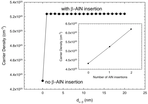
Fig. 2 shows the change in carrier density with the
change of dα-β. A dramatic increase in carrier density is
calculated with the inclusion of β-AlN layer. The position of β-AlN layer can only disturb the carrier density of the structure. No significant change in 2DEG probability density was observed. Therefore, we can conclude that the only inclusion of the β-AlN layer improves the carrier density, not the position. Experimentally, inserting an AlN layer in an InAlN layer is difficult to achieve experimentally due to the difference in growth temperatures of the AlN and InAlN layers [23]. Therefore,
we accept the dα-β = 20 nm case (two AlN layers at the
sides of an InAlN barrier layer) as an optimum structure. This kind of insertion was experimentally used by Dadgar et al. [10]. The strain value induced by this layer is much lower than the value needed for strain relaxation, so that this layer can be pseudomorphically grown on an
In0.18Al0.82N layer from an experimental point of view. In
the Figure 2 insert, the effect of the inclusion of a third AlN layer (hereinafter referred to as γ-AlN) in an
In0.18Al0.82N layer is shown. The strain values are still far
for a strain relaxation for an experimental study. A linear increase in the carrier density was observed with every AlN insertion. However, the insertion of a high temperature γ-AlN layer in a low temperature grown InAlN barrier layer is difficult to achieve experimentally as pointed out above [23]. If we assume that all the
906 S. B. Lisesivdin, E. Ozbay
technological challenges that are associated with the reliable growth of this type of structure can be solved,
higher carrier densities can be obtained with an engineered SIS like barrier.
d
α−β(nm)
0 5 10 15 20 25C
a
rr
ier
De
ns
it
y
(
c
m
-3)
4.2x10²⁰ 4.4x10²⁰ 4.6x10²⁰ 4.8x10²⁰ 5.0x10²⁰ 5.2x10²⁰ 5.4x10²⁰no β-AlN insertion
Number of AlN insertionsC a rrier Density (cm -3 ) 4.0x10²⁰ 4.5x10²⁰ 5.0x10²⁰ 5.5x10²⁰ 6.0x10²⁰ 6.5x10²⁰ 0 1 2
with β-AlN insertion
Fig. 2. Carrier density versus distance between the α-AlN and β-AlN layers. The figure also includes the case with the β-AlN layer. Insert: Carrier density versus the number of AlN layer insertions.
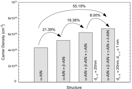
Up to this point, with β-AlN (dα-β = 20 nm) and γ-AlN
layer insertions in the barrier layer, a 21.39% and additional 18.38% increase in the carrier density is predicted, respectively. To investigate the effects of an AlN insertion in a GaN layer on the carrier density, we included an additional AlN (hereinafter referred to as δ-AlN) in GaN layer. Fig. 3 shows the band diagram of the investigated structure in the case of δ-AlN insertion. Here,
dα-δ is the distance between the α-AlN and δ-AlN layers. In
the Fig. 3 insert, band diagram for dα-δ = 1 nm case is
shown. In this case, the α-AlN well is above the Fermi
level, so that it is not populated. With the increasing dα-δ,
the α-AlN well begins to populate and the δ-AlN well depopulates as shown in Fig. 4. In this figure, the total carrier density is shown with a red line. The most
important increase in the carrier density is observed for d
α-δ = 1 nm case. A second important increase was observed
at dα-δ = 5-6 nm case. z (nm) 0 10 20 30 40 50 Ec (e V) 0 2 4 6 8 No δ-AlN insertion With δ-AlN insertion Fermi Level dα−δ δ-AlN α-AlN γ-AlN β-AlN z (nm) 24 25 26 27 28 29 30 E (ec V ) -1 0 1 2 3 EF EF dα−δ =1 nm
Fig. 3. Band diagram after inserting the δ-AlN layer.
Effect of various pseudomorphic AlN layer insertions on the electron densities of two-dimensional electron gas … 907 dα−δ (nm) -2 0 2 4 6 8 10 12 C a rrie r De ns ity ( c m -3) 1020 2x10²⁰ 3x10²⁰ 4x10²⁰ 5x10²⁰ 6x10²⁰ 7x10²⁰ Single well α-AlN well δ-AlN well Total
Fig. 4. Carrier densities of α-AlN well, δ-AlN well and
the total of these two wells with respect to dα-δ. No δ-AlN
well inserted case is shown as a triangle.
After dα-δ = 6 nm, the carrier density was dramatically
decreased due to the total depopulation of the δ-AlN well. The carrier density gains in every step, which were investigated up to now, are shown in Fig. 5. In the figure,
dα-β = 20 nm and dα-δ = 1 nm are selected for the last two
steps. Structure C a rr ie r D e n s it y (c m -3 ) 2x10²⁰ 4x10²⁰ 6x10²⁰ 8x10²⁰ 1021 α -A lN α-A lN + β-A lN α -A lN + β-A lN + γ-A lN α-A lN + β-A lN + γ-A lN + δ-A lN dα− β = 2 0nm dα− β = 2 0nm , d α− δ = 1 nm 0 21.39% 18.38% 8.00% 55.19%
Fig. 5. Carrier density gains for the investigated structures.
A higher carrier density is an important parameter for high power applications. However, higher mobility is also an important parameter for high performance [24]. For the δ-AlN layer inserted case, both quantum wells were
observed to have changing well widths with respect to dα-δ.
The quantum well width (Z0) is a parameter that influences
three important 2D scattering mechanisms: Background
impurity (BI) scattering (
µ
BI∝ Z
0−1) [25], interfaceroughness (IFR) scattering (
µ
IFR∝
Z
06) [26, 27], andpolar optical phonon (PO) scattering (
µ
PO∝ Z
0−1) [28].In order to investigate the effects of the Z0 to mobility, we
firstly calculate the Z0 with respect to dα-δ. We used the full
width at half maximum (FWHM) values of the carrier
density distributions in quantum wells as Z0, as shown in
the Fig. 6 insert.
dα−δ (nm) -2 0 2 4 6 8 10 12 Q ua n tum w e ll w id th (Z 0 ) (nm ) 0.8 1.0 1.2 1.4 1.6 1.8 2.0 Single well α-AlN well δ-AlN well α-AlN well δ-AlN well
Fig. 6. Quantum well widths of α-AlN well, δ-AlN well
with respect to dα-δ. No δ-AlN well inserted case is shown
as a triangle. Insert: FWHM’s of the carrier density distributions.
908 S. B. Lisesivdin, E. Ozbay
Fig. 6 shows the Z0 of the α-AlN well and the δ-AlN
well with respect to dα-δ. With the increasing dα-δ, the well
widths of both quantum wells increase notably until dα-δ =
6 nm. At low temperatures, IFR can be accepted as the dominant scattering mechanism [29]. As seen from the
figure, dα-δ = 1 nm case, which has the highest carrier
density value, will be scattered by the IFR mechanism more than the other cases at low temperatures because of the well width. At high temperatures – such as room temperature – PO is known to be the dominant scattering mechanism. With the increasing quantum well width, PO scattering is more effective. As a result, δ-AlN layer insertion not only affects the carrier density, but is also affects the mobilities of the carriers. With experimentally
smooth interfaces, dα-δ = 1 nm case will provide an
additional 8% carrier increase with respect to the β-AlN
(dα-β = 20 nm) and γ-AlN layer inserted structure.
Otherwise, δ-AlN layer insertion may conclude a decrease in conduction due to low mobilities.
4. Conclusions
We have modeled the effects of various 1 nm pseudomorphic AlN layer insertions in lattice-matched
In0.18Al0.82N/GaN based heterostructures with
self-consistent solutions of non-linear Schrödinger-Poisson equations. The band structures and sheet carrier densities for each layer insertion were calculated. In addition, the effects of the position and number of the AlN insertions on the carrier densities were investigated. Our computer simulations showed an important increase in the carrier density with the increasing number of AlN insertions in an
In0.18Al0.82N barrier. For a technological foresight,
pseudomorphic grown SIS-like barriers with use of AlN
insertions in an In0.18Al0.82N layer can be proposed for
future investigations. It will be a challenging process due to the different optimum growth temperatures of the AlN
and In0.18Al0.82N layers. Instead of an SIS-like barrier, two
AlN insertions at the sides of the barrier layer have come into prominence because of the experimental applicability. According to the simulations, insertion in the GaN layer does not have a major effect on the carrier density. According to the simulations, an AlN layer insertion in the GaN layer with distances of 1 nm and 6 nm with respect to
an In0.18Al0.82N/GaN interface provide additional carriers.
However, because the introduction of an AlN layer insertion in a GaN layer will also negatively affect the mobility, the total conductivity may be lower in total. These simulation results are important figures of merit in order to experimentally obtain higher carrier densities in GaN-based heterostructures. Future experimental explorations involving pseudomorphic growths could cast a definitive answer in terms of carrier density and mobility, which is, however, beyond the scope of the present paper.
Acknowledgements
This work is supported by the European Union under the projects EU-PHOME, and EU-ECONAM, and TUBITAK under Project Nos. 106E198, 107A004, and 107A012. One of the authors (E.O.) also acknowledges partial support from the Turkish Academy of Sciences.
References
[1] H. Morkoç, Handbook of Nitride Semiconductors and Devices I-III., Wiley-VCH, New York, 2008. [2] M. A. Khan, J. N. Kuznia, J. M. V. Hove, N. Pan, J. Carter, Appl. Phys. Lett. 60, 3027 (1992).
[3] I. P. Smorchkova, S. Keller, S. Heikman, C. R. Elsass, B. Heying, P. Fini, J. S. Speck, U. K. Mishra, Appl. Phys. Lett. 77, 3998 (2000).
[4] I. P. Smorchkova, L. Chen, T. Mates, L. Shen, S. Heikman, B. Moran, S. Keller, S. P. DenBaars, J. S. Speck, U. K. Mishra, J. Appl. Phys. 90, 5196 (2001). [5] Y. –F. Wu, A. Saxler, M. Moore, R. P. Smith, S. Sheppard, P. M. Chavarkar, T. Wisleder, U. K. Mishra, P. Parikh, IEEE Electron Device Lett. 25, 117 (2004).
[6] S. B. Lisesivdin, A. Yildiz, M. Kasap, Optoelectron. Adv. Mater. – Rapid Comm. 1, 467 (2007).
[7] O. Ambacher, B. Foutz, J. Smart, J. R. Shealy, N. G. Weimann, K. Chu, M. Murphy, A. J. Sierakowski, W. J. Schaff, L. F. Eastman, J. Appl. Phys. 87, 334 (2000).
[8] S. Arulkumaran, T. Egawa, H. Ishikawa, T. Jimbo, J. Vac. Sci. Technol. B 21, 888 (2003).
[9] J. Kuzmik, IEEE Electron Device Lett. 22, 510 (2001).
[10] A. Dadgar, F. Schulze, J. Bläsing, A. Diez, A. Krost, M. Neuburger, E. Kohn, I. Daumiller, M. Kunze, Appl. Phys. Lett. 85, 5400 (2004).
[11] M. Gonscherek, J. -F. Carlin, E. Feltin, M. A. Py, N. Grandjean, V. Darakchieva, B. Monemar, M. Lorenz, G. Ramm, J. Appl. Phys. 103, 093714 (2008). [12] F. Medjdoub, D. Ducatteau, C. Gaquiere, J. -F. Carlin, M. Gonschorek, E. Feltin, M. A. Py, N. Grandjean, E. Kohn, Electron. Lett. 43, 71 (2007). [13] J. Xie, X. Ni, M. Wu, J. H. Leach, U. Ozgur, H. Morkoc, Appl. Phys. Lett. 91, 132116 (2007). [14] A. Bykhovski, B. Gelmont, M. Shur, J. Appl. Phys. 81, 6332 (1997).
[15] S. Birner, S. Hackenbuchner, M. Sabathil, G. Zandler, J. A. Majewski, T. Andlauer, T. Zibold, R. Morschl, A. Trellakis, P. Vogl, Acta Phys. Pol. A 110, 111 (2006).
[16] I. Vurgaftman, J. R. Meyer, L. R. Ram-Mohan, J. Appl. Phys. 89, 5815 (2001).
[17] I. Vurgaftman, J. R. Meyer, J. Appl. Phys. 94, 3675 (2003).
Effect of various pseudomorphic AlN layer insertions on the electron densities of two-dimensional electron gas … 909
[18] O. Ambacher, J. Majewski, C. Miskys, A. Link, M. Hermann, M. Eickhoff, M. Stutzmann, F. Bernardini, V. Fiorentini, V. Tilak, B. Schaff, L. F. Eastman, J. Phys.: Condens. Matter 14, 3399 (2002).
[19] H. Morkoç, Nitride Semiconductors and Devices, Springer-Verlag, Berlin Heidelberg 1999. [20] J. Singh, Physics of Semiconductors and Their Heterostructures, McGraw-Hill, New York, 1992, p. 734.
[21] B. Jogai, J. Appl. Phys. 93, 1631 (2003).
[22] S. Heikman, S. Keller, Y. –F. Wu, J. S. Speck, S. P. DenBaars, U. K. Mishra, J. Appl. Phys. 93, 10114 (2003).
[23] J. Bläsing, A. Reiher, A. Dadgar, A. Diez, A. Krost, Appl. Phys. Lett. 81, 2722 (2002).
[24] C. Skierbiszewski, K. Dybko, W. Knap, M. Siekacz, W. Krupczynski, G. Nowak, M. Bockowski, J. Łusakowski, Z. R. Wasilewski, D. Maude, T. Suski, S. Porowski, Appl. Phys. Lett. 86, 102106 (2005). [25] K. Hess, Appl. Phys. Lett. 35, 484 (1979). [26] H. Sakaki, T. Noda, K. Hirakawa, M. Tanaka, T. Matsusue, Appl. Phys. Lett. 51, 1934 (1987). [27] J. M. Li, J. J. Wu, X.X. Han, Y. W. Lu, X. L. Liu, Q. S. Zhu, Z. G. Wang, Semicond. Sci. Technol. 20, 1207 (2005).
[28] B. K. Ridley, J. Phys. C: Solid State Phys. 15, 5899 (1982).
[29] D. Zanato, S. Gokden, N. Balkan, B. K. Ridley, W. J. Schaff, Semicond. Sci. Technol. 19, 427 (2004).
__________________________
*Corresponding author: [email protected]
View publication stats View publication stats