Highly directive radiation and negative refraction
using photonic crystals
Article in Laser Physics · February 2005 CITATIONS6
READS23
6 authors, including: Some of the authors of this publication are also working on these related projects: MetasurfacesView project Loss compensation of plasmonic losses
View project Ekmel Ozbay Bilkent University 633 PUBLICATIONS 15,187 CITATIONS SEE PROFILE Irfan Bulu Schlumberger Limited 97 PUBLICATIONS 2,261 CITATIONS SEE PROFILE Koray Aydin Northwestern University 121 PUBLICATIONS 4,849 CITATIONS SEE PROFILE Kamil Boratay Alici TUBITAK Space Technologies Research Institute 47 PUBLICATIONS 1,297 CITATIONS SEE PROFILE
All content following this page was uploaded by Irfan Bulu on 04 October 2017. The user has requested enhancement of the downloaded file.
Laser Physics, Vol. 15, No. 2, 2005, pp. 217–224.
Original Text Copyright © 2005 by Astro, Ltd.
Copyright © 2005 by MAIK “Nauka /Interperiodica” (Russia).
1. INTRODUCTION
Photonic crystals (PCs) are periodic dielectric or metallic structures in which the periodicity gives rise to bands for the propagation of electromagnetic waves and to band gaps where propagation is prohibited for certain frequency range [1]. The investigation of optical properties at the band-gap edges and of the cavity (defect) modes has expanded rapidly into applications in photonic devices [2]. Using different materials (i.e., with different dielectric constants) and by adjusting the geometrical parameters of the crystal, the band struc-ture and, hence, the propagation of light can be modi-fied virtually in any way in a controllable manner. The scale-invariant nature of the governing Maxwell’s equations enables the study of electromagnetic (EM) phenomena without being held back by structural com-plexities. Another advantage is also present from a dimensionality point of view; that is, the lack of con-finement in certain spatial directions in 2D or 1D PC structures does not hinder the investigation of the EM phenomena.
The enormous possibilities for applications in tele-communications and the optical wavelength scale drive the investigation of PCs towards the micro- and nanos-cales [3–7]. Various fabrication techniques have been investigated in the last decade, including alternating layer deposition and an etching process for 3D PCs [8] and electron lithography in combination with dry etch-ing for 2D AlGaAs PCs [9] to realize the photonic crys-tal structures at these scales. So far, keeping the struc-tural uniformity, particularly in 3D, appears to be the most challenging problem.
In this paper, we review certain optical properties of PCs. First, we discuss how a 2D PC can be utilized to obtain highly directive radiation from embedded sources, which has particular importance for antenna applications. In the second part of the article, we present an experimental demonstration and simulation of a completely novel optical phenomenon, namely, negative refraction and subwavelength focusing through a 2D PC slab.
Highly Directive Radiation and Negative Refraction
Using Photonic Crystals
E. Ozbay
1, 2,*, I. Bulu
1, K. Aydin
1, H. Caglayan
1, K. B. Alici
1, and K. Guven
1 1 Department of Physics, Bilkent University, Bilkent, 06800 Ankara, Turkey2 Nanotechnology Research Center, Bilkent University, Bilkent, 06800 Ankara, Turkey
*e-mail: [email protected] Received September 2, 2004
Abstract—In this article, we present an experimental and numerical study of certain optical properties of two-dimensional dielectric photonic crystals (PCs). By modifying the band structure of a two-two-dimensional photonic crystal through its crystal parameters, we show how it is possible to confine the angular distribution of radiation from an embedded omnidirectional source. We then demonstrate that the anomalous band dispersions of PCs give rise to completely novel optical phenomena, in particular, the negative refraction of electromagnetic waves at the interface of a PC. We investigate the spectral negative refraction, which utilizes a transverse magnetic (TM)-polarized upper band of a PC, in detail and show that a high degree of isotropy can be achieved for the corresponding effective index of refraction. The presence of nearly a isotropic negative refractive index leads to focusing of omnidirectional sources by a PC slab lens, which can surpass certain limitations of conventional (positive refractive) lenses. These examples indicate the potential of PCs for photonics applications utilizing the band structure.
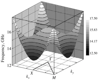
12.50 14.17 15.83 17.50 M X Γ ky kx 16 14 12 Frequency, GHz
Fig. 1. The TM-polarized second band of the PC in the first Brillouin zone.
MODERN TRENDS
IN LASER PHYSICS
218
LASER PHYSICS Vol. 15 No. 2 2005
OZBAY et al.
2. HIGHLY DIRECTIONAL RADIATION FROM SOURCES EMBEDDED
IN TWO-DIMENSIONAL PHOTONIC CRYSTALS Spatial confinement of the radiation emitted by sources is highly desirable for certain antenna applica-tions. Several studies have investigated the use of PCs for the confinement of radiation as a cover for the source [10–12] or for the source being embedded inside the PC [13, 14]. The mechanism is based essentially on the coupling of electromagnetic waves emitted by the source to a certain band of the PC, where the dispersion of the band enables one to confine the propagating power spatially to a very narrow region.
We investigate a 2D photonic crystal consisting of a square array of cylindrical alumina rods. The rods have a radius of 1.55 mm and a dielectric constant of 9.61. The crystal period is 11.0 mm. The band structure of the corresponding infinite PC for TM-polarized EM waves is given in Fig. 1. We observe that, at the mini-mum of the second band (upper band), only the modes
along Γ–X' are allowed to propagate inside the PC,
where X' represents all directions with the same sym-metry properties as the X point. For the modes near the upper-band edge, k|| = kx ≈ 0. Apart from an additive
reciprocal lattice vector, k|| is conserved at the air–PC interface [15]. Therefore, we conclude that, for a source embedded inside the PC and operating at the upper-band-edge frequency, the emitted waves should be transmitted from the PC to air only along the Γ–X direc-tion. In addition, the modes near the upper-band edge are air modes; i.e., most of the energy of the EM waves is concentrated in the low-dielectric-material region as the waves propagate through the PC, as can be seen in Fig. 2a. When the waves near the upper-band edge emerge from the surface of the PC, most of the power will flow through the low-dielectric-material region of the PC (Fig. 2b). Thus, the exit points may be regarded as an array of radiation sources.
Delay-time measurements of the present PC struc-ture shown in Fig. 3a indicate that the group velocity near the upper-band edge is reduced by up to 22 times in comparison to air. Delay time is defined as tp = ∂ϕ/∂ω, where ϕ is the difference between the phase of the EM wave inside the PC and in free space. Since at the upper-band edge the modes are allowed to propa-gate only along Γ–X', these radiation sources will have a uniform distribution of phase differences. Therefore, the surface of the PC can be regarded as an antenna array operating at the upper-band-edge frequency with similar spatial and temporal distribution of power and a uniform phase difference. Consequently, the power radiating in the Γ–X direction from the surface is antic-ipated to be highly confined.
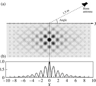
The experimental observation of the confined radia-tion is performed by the setup depicted in Fig. 2a. A monopole antenna is inserted into the 2D PC as an omnidirectional source. A HP-8510C network analyzer is used to excite the monopole source and to measure
0.5 X 0 1.0 –8 –6 –4 –2 0 2 4 6 8 10 –10 Angle Horn antenna 1.5 m X (b) (a)
Fig. 2. (a) Experiment setup for a 2D 20 × 10 square-array PC. The electric-field-intensity distribution of a source located at the center and operating at the second band-edge frequency. Note that the field is localized between the dielectric rods (air). (b) Lateral distribution of the electric-field intensity along the upper surface of the PC.
–45 13.1 13.0 –30 105 90 13.2 13.3 13.4 –30 –15 0 10 20 Transmission Photon lifetime
Transmission, dB Delay time, ns
Frequency, GHz (a) (b) 120 135 75 60 45 Angle, deg –15 0 Intensity, dB 13.15 GHz 13.25 GHz 13.30 GHz Band edge
Fig. 3. (a) The transmission and delay time measured near the upper-band edge of the PC. (b) The far-field radiation patterns of various frequencies in the upper band emitted from the PC surface perpendicular to the ΓX direction.
HIGHLY DIRECTIVE RADIATION AND NEGATIVE REFRACTION 219
the power emitted from the monopole source. The mea-sured far-field radiation patterns for a square array of
32 × 20 alumina rods at various frequencies near the
upper-band edge are presented in Fig. 3b. The mini-mum half-power beam width is obtained at 13.21 GHz and found to be 8°. This also corresponds to the maxi-mum delay time, as shown in Fig. 3a. Hence, we con-clude that the upper-band edge is at 13.21 GHz. It is evident that the angular distribution of power strongly depends on the radiation frequency. The radiation pat-terns spread quickly for frequencies lying deep in the upper band. This can be explained by the presence of equal frequency modes along different directions at these frequencies.
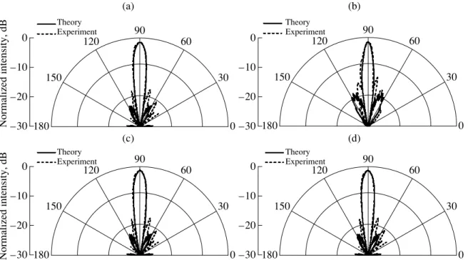
The measured and calculated far-field radiation pat-terns for different PC lateral lengths are presented in Fig. 4. The measured half-power beam widths show an optimum crystal length, which is found to be 24 layers,
corresponding to a beam width of 6°. This beam width
is a significantly small value among those reported so far for PC embedded sources. The deviations from the optimum value affect both the radiation pattern and the half-power beam widths. The change is more signifi-cant when the lateral length is decreased from its opti-mum value. This can be explained by the fact that the strength of the surface radiators decreases rapidly away from the center of the PC, as indicated in Fig. 2b. Con-sequently, increasing the lateral length (adding more but weaker surface radiators) is less significant com-pared to the effect of decreasing it (removing stronger surface radiators).
3. NEGATIVE REFRACTION AND POINT FOCUSING
THROUGH A PHOTONIC CRYSTAL SLAB In the previous section, the modification of the radi-ation pattern of a point source embedded inside a PC by utilizing the photonic band structure is exemplified. However, there is more that the PCs can provide. In this section, we present a striking example of the novel opti-cal phenomena that are unveiled by PCs.
In 1960, Veselago proposed and investigated the electrodynamics in a medium possessing a negative index of refraction [16]. The realization of such a medium has become a subject of interest recently, albeit using artificial composite structures with negative per-mittivity and negative permeability, respectively [17– 20].
At the same time, several studies reported anoma-lous refraction behavior at the PC interfaces that was called the “superprism phenomenon” [21–23]. It has been found that the PCs can exhibit unusual propaga-tion characteristics that resemble that of a medium with a negative effective index of refraction. Further analysis of the band structures of PCs revealed the underlying mechanisms for negative refraction. In one mechanism, the incident field couples to a band with convex equal
frequency contours (EFCs) in k-space, where the
con-servation of the surface-parallel component of the wavevector, k, combined with the “negative” curvature of the band causes the incident beam to bend negatively [22, 24]. In this case, however, neither the group veloc-ity nor the effective index is negative, and the PC is
–20 –30 –10 0 120 90 150 180 60 30 0 Theory Experiment 90 120 150 180 60 30 0 90 120 150 180 60 30 0 90 120 150 180 60 30 0 –20 –30 –10 0 –20 –30 –10 0 –20 –30 –10 0 Theory Experiment Theory Experiment Theory Experiment (a) (c) (d) (b) Normalized intensity, dB Normalized intensity, dB
Fig. 4. Measured (dashed curves) and simulated (solid curves) far-field patterns at the upper-band-edge frequency of 13.21 GHz for different lateral lengths of the PC: (a) 32 × 16, (b) 28 × 16, (c) 24 × 16, and (d) 20 × 16 layers.
220
LASER PHYSICS Vol. 15 No. 2 2005
OZBAY et al.
essentially a positive-index medium exhibiting nega-tive refraction. Alternanega-tively, if the group velocity and phase velocity derived from the band dispersion are antiparallel for all values of k, the effective index of refraction of the PC becomes negative for that particu-lar frequency range of the band [25]. Both mechanisms have been confirmed experimentally [26, 27].
The interest in negative refraction phenomenon does not stem only from a fundamental-physics point of view. Pendry [28] proposed that negative neff in
left-handed materials can be used for constructing a perfect lens, one which is not limited by diffraction. Subwave-length imaging in PCs is studied in detail theoretically in [29]. Later, Cubukcu et al. [26] demonstrated exper-imentally subwavelength resolution along a 2D PC–air
interface. Recently, Parimi et al. [27] demonstrated
the near-field image formation of a point source with a 2D PC.
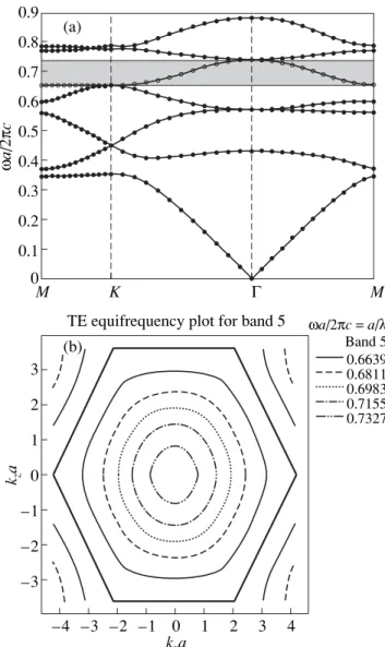
Following the analysis presented in [25], we con-struct a PC and utilize a TE-polarized upper band to achieve a negative effective index of refraction (neff).
The photonic crystal is a hexagonal lattice of alumina rods in air with a lattice period of a = 4.79 mm. The rods have dielectric constant ε = 9.61, diameter 2r =
3.15 mm, and length l = 15 cm. Figure 5a shows the
transverse electric (TE)-polarized band structure in the first Brillouin zone. The transverse direction is taken to be in the plane of the 2D photonic crystal. The fifth band, shaded in the figure, extends from = 0.65 (f =
40.65 GHz) to = 0.74 (f = 46.27 GHz), where =
fa/c is the scaled frequency. In Fig. 5b, the equal-fre-quency contours (EFCs) in the full Brillouin zone are plotted. The EFCs of the band shrink with increasing frequency, contrary to the EFCs in air (n = 1), which are given by the dispersion ω = ck. As a result, the effective refractive index np = sgn( · )(c| |/ω) becomes negative due to the sign of the antiparallel group
veloc-ity = and the phase velocity = (c/|np|) .
Here, c is the speed of light in vacuum and is the unit wavevector in the PC.
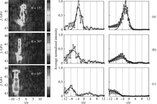
The refraction spectra are measured by a setup con-sisting of a network analyzer, a microwave horn antenna as the transmitter, and a waveguide antenna as the receiver. The PC has seven layers along the inci-dence (ΓM) direction and 31 layers along the lateral (ΓK) direction. The horn antenna is located on the neg-ative side of the PC with respect to its central axis. The spatial intensity distribution along the PC–air interface is scanned in 1.27-mm steps, while the frequency is swept from 38.5 to 43.5 GHz. Figure 6a displays the transmission spectra as a function of frequency and lat-eral position for three different incidence angles θi = 15°, 30°, and 45°. It is evident that the transmitted beam appears on the negative side. We observe that the anisotropy due to frequency dependence causes some spatial broadening. When the incidence angle is increased, the transmission shifts left accordingly. To investigate the beam profiles, the spatial cross sections at f = 41.7 GHz ( = 0.667) are plotted in Fig. 6b. We remind the reader that the incident field has a Gaussian beam profile centered at x = 0 (not shown in the fig-ures). The intensities are normalized with respect to the maximum intensity for the 15° incidence. It is apparent that the lateral shift is accompanied by a decrease in the transmission intensity. This can be attributed to the higher reflection at the interface for larger incidence angles and to the diffraction-induced out-of-plane losses, which increase with increasing path length through the lattice. Figure 6c displays the correspond-ing profiles obtained from FDTD simulations, which show very good agreement with measurements.
f˜ f˜ f˜ vg kf kf vg ∇ kω vp kˆf kˆf f˜ 0.9 0.8 0.7 0.6 0.5 0.4 0.3 0.2 0.1 0 M K Γ M ω a /2 π c (a) 3 2 1 0 –1 –2 –3 –4 –3 –2 –1 0 1 2 3 4 kxa kz a Band 5 0.6639 0.6811 0.6983 0.7155 0.7327 ωa/2πc = a/λ
TE equifrequency plot for band 5 (b)
Fig. 5. (a) TE-polarized band diagram of the PC. The fifth
band, which has a negative effective refractive index, is shaded. (b) Equal-frequency contours of the fifth band in the full Brillouin zone. Note that the contours are nearly cir-cular (i.e., isotropic) and shrink with increasing frequency.
HIGHLY DIRECTIVE RADIATION AND NEGATIVE REFRACTION 221
In order to gain insight into the propagating field within the crystal, we performed a FDTD simulation for the θi = 30° incidence, which is shown in Fig. 7.
Evidently, higher order reflection (marked 3) is present because, at this frequency of the incident field ( = 0.667), the condition ≤ a/(2ainterface) is not met [24, 29]. Here, ainterface is the interface period of the PC. The
refracted beam (marked 4), however, appears to be a single component, which can also be inferred from the single transmitted component on the other side of the PC (marked 5). We have found that a single refracted beam is present for incidence angles θi ≤ 45° at this band for the present PC. Previous studies also pointed out that single beam refraction at higher bands is possi-ble [22, 25, 30]. We therefore assume that most of the propagating power is coupled to the zeroth-order dif-fracted wave and employ Snell’s law for this geometry:
n( f, ki)sinθf = nairsinθi, where θi is the angle of
inci-dence and θf is the angle of refraction inside the
photo-nic crystal. For θi = 15°, 30°, and 45°, we obtain neff =
–0.52, –0.66, and –0.86 from the experiment, respec-tively. The simulation results for the same incidence angles give neff = –0.66, –0.72, and –0.80, respectively.
The anisotropy of the effective refractive index is evi-dent from these figures, but the variation occurs within
f˜ f˜
a margin that is small when contrasted to the wide frequency range (~3-GHz width) of the negative refraction. 0.5 0 –8 x/a –12 –4 0 4 8 12 1.0 –8 x/a –12 –4 0 4 8 12 0.5 0 1.0 0.5 0 1.0 –10 –5 0 5 10 40 41 42 43 f, GFz 40 41 42 43 f, GFz 40 41 42 43 f, GFz θ = 15° θ = 30° θ = 45°
Average normalized intensity
Fig. 6. (a) Measured negative refraction spectra of the fifth band along the PC–air interface for incidence angles θ = 15°, 30°, and 45°. Measured (b) and simulated (c) intensity profiles at f = 41.7 GHz for the respective incidence angles. Solid curves indicate Gaussian fits.
1 2
3
4 5
Fig. 7. Simulated negative refraction of a plane wave at f =
41.7 GHz incident at θ = 30° to the PC interface (mark 1). Zeroth-order (mark 2) and higher order (mark 3) reflections occur. The refracted (mark 4) and the transmitted (mark 5) components appear to propagate as single beams.
x/a
(a)
(b)
LASER PHYSICS Vol. 15 No. 2 2005
The presence of negative refraction for a large range of incidence angles is accompanied by the possibility that the slab structure may act like a lens for an omnidi-rectional source. For the present PC, we first performed FDTD simulations for a TE-polarized point source at
f = 42.07 GHz, located at a distance dsrc = 2λ away from
the air–PC interface. We note that the previous studies investigated the case in which the source is located in the vicinity of the PC interface (dsrc < λ) [26, 27].
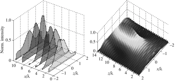
Fig-ure 8b shows the resulting normalized spatial intensity distribution in the image plane. The PC–air interface is located at z = 0. The peak unambiguously indicates focusing behavior (we also refer the reader to Fig. 10
for the simulated 2D field map, where the convergence of wavefronts to a focal point along the optical axis is clearly visible). We would like to emphasize that the focusing occurs away from the PC–air interface, with an enhancement of ~12 dB compared to free space at
z ≈ 8λ. This is a very high value among those reported so far concerning focusing through PC structures. In this respect, channeling-induced focusing effects that occur close to the interface may also be excluded.
In the experiment, a waveguide aperture is used as the source, and the intensity distribution in the image plane is measured by a monopole antenna. For dsrc = 2λ,
first the propagation direction, z, is scanned to locate the maximum intensity, and then lateral cross sections of intensity at several z values around the peak position are measured. In Fig. 8a, the focusing of the beam both in the lateral and longitudinal directions is evident. The maximum intensity (normalized to unity) is observed at
dfocus/λ≈ 8. We note that the measured and simulated
focusing profiles are quite similar.
The presence of the flat-lens behavior of the PC structures has been discussed in recent studies [27]. In this case, the focused-field profile should mimic the arbitrary lateral shifts of the source along the interface. Although this may appear trivial, the focusing behav-iors in some PC structures are reported to depend on whether the source is located directly in front of a dielectric rod at the interface or elsewhere. Here, we confirm by experiment and simulations that the present structure behaves as a perfect flat lens. In Fig. 9, the source positions (vertical dashed lines) and the peak positions of the focused beam (symbols) are found to shift exactly by the same amount. Furthermore, the simulated profiles (solid curves) using a true point source show a remarkable match with the measured data. We therefore conclude that, for dscr on the order of
several λ, the waveguide aperture provides a good
10 8 6 4 2 0 –2 –1 0 1 2 1.0 0.5 0 Norm. intensity 1.0 0.5 0 14 12 10 8 6 4 2 0 1 2 –1 –2 x/λ z/λ z/λ x/λ
Fig. 8. (a) Lateral intensity profiles measured at six different positions along the propagation direction: z/λ = 1.78, 3.56, 5.34, 7.12, 8.90, and 10.68. (b) Simulated 2D intensity in the image plane. z = 0 corresponds to the PC interface.
0.1
–1
Norm. avg. intensity
x/a –2 –3 0 1 2 3 4 5 6 0.2 0.3 0.4 0.5 0.6 0.7 0.8 0.9 1.0 0 ∆x/a = 0 ∆x/a = 0.26 ∆x/a = 1.06 ∆x/a = 2.12
Fig. 9. The measured (symbols) and simulated (solid
curves) lateral intensity profiles at the focal distance (z/λ≈ 8) for different lateral shifts. The respective source locations are denoted by vertical dashed lines.
HIGHLY DIRECTIVE RADIATION AND NEGATIVE REFRACTION 223
approximation to a point source. The average FWHM of the profiles at dfocus≈ 8λ depicted in Fig. 9 is 1.60a ≈
1.08λ, on par with λ. We alert the reader that a
sub-wavelength focusing as discussed in recent studies is not considered here [29]. Subwavelength focusing requires the amplification of evanescent waves through the photonic crystal for image formation. This implies an upper limit on the location of the source and image from the PC, since the evanescent waves decay rapidly away from the interfaces.
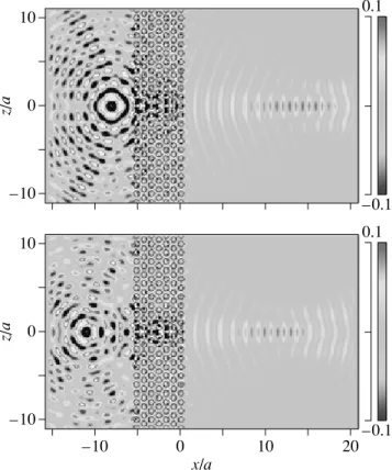
In a manner similar to the lateral shift, the shift of the source along the longitudinal direction is expected to be followed by the focus pattern. The FDTD-simu-lated 2D map of the magnetic field, Hy(x, z), plotted in
Fig. 10 shows this behavior clearly: when the source is moved away from dscr = 2λ to dsrc = 4λ, the focus pat-tern shifts towards the PC–air interface. Finally, in Fig. 11, the measured lateral profiles at the respective focal points for various dsrc are plotted. From the
deter-mined focal positions, we found that (dsrc + dfocus) remains roughly constant. The figure also displays the intensity profile in the absence of the PC for dsrc = 2λ case (dotted line). At the focal distance, the intensity is almost a flat line with no features indicating the source location; hence, enhancement by focusing is evident.
4. CONCLUSIONS
In this article, we presented certain optical proper-ties of PC structures. The improvement of existing opti-cal applications by PCs is exemplified by the excep-tional directivity of radiation from an omnidirecexcep-tional source embedded in a PC, which is an important feature for antenna applications. We then discussed a novel and unusual optical phenomenon observed in PCs, namely, negative refraction. This phenomenon may lead to novel lens structures that will surpass the limitations of conventional (i.e., positive-refractive) lenses. We would like to emphasize that the electromagnetic phenomena investigated here depend only on the refractive index of the dielectric material and on the geometrical parame-ters of the 2D PC. Hence, their scalability across the entire electromagnetic spectrum makes them poten-tially available for a wide range of applications. Based on this fact, photonic crystal structures are anticipated to be an essential component of photonic integrated cir-cuits in the near future.
REFERENCES
1. J. D. Joannopoulos, R. D. Maede, and J. N. Winn,
Pho-tonic Crystals: Molding the Flow of Light (Princeton
Univ. Press, Princeton, N.J., 1995).
2. Photonic Crystals and Light Localization in the 21st
Century, Ed. by C. Soukoulis (Kluwer, Dordrecht,
2000).
3. H. Benisty, C. Weisbuch, D. Labilloy, et al., J. Lightwave Technol. 17, 2063 (1999).
4. T. Krauss, Y. P. Song, S. Thomson, et al., Electron. Lett. 30, 1444 (1994).
5. P. L. Gourley, J. R. Wendt, G. A. Vawter, et al., Appl. Phys. Lett. 64, 687 (1994).
0.1
Norm. avg. intensity
x/λ –2 –3 3 0.2 0.3 0.4 0.5 0.6 0.7 0.8 0.9 1.0 0 dsrc = 2λ, dfcs ~ 8λ –1 0 1 2 dsrc = 4λ, dfcs ~ 6.2λ dsrc = 6λ, dfcs ~ 4.9λ dsrc = 2λ, no PC
Fig. 11. The measured lateral intensity profiles at respective
focal distances for different source distances. The intensity axis is normalized by the dsrc = 2.0λ profile peak. The dashed line denotes the intensity profile in the absence of a PC for dsrc = 2λ. 10 0 –10 z/ a 0.1 –0.1 10 0 –10 z/ a 0.1 –0.1 –10 0 10 20 x/a
Fig. 10. Simulated 2D magnetic-field distribution Hy(x, z) for dsrc = 2λ (top) and dsrc = 4λ (bottom).
LASER PHYSICS Vol. 15 No. 2 2005
Electron. 38, 726 (2002).
7. J. M. Lourtioz, H. Benisty, A. Chelnokov, et al., Ann. Telecommun. 58, 1197 (2003).
8. E. Kuramochi, M. Notomi, T. Kawashima, et al., Opt. Quantum Electron. 34, 53 (2002).
9. Y. Sugimoto, N. Ikeda, N. Carlsson, et al., J. Appl. Phys. 91, 922 (2002).
10. E. R. Brown, C. D. Parker, and E. Yablonovitch, J. Opt. Soc. Am. B 61, 404 (1993).
11. R. Gonzalo, P. De Maagt, and M. Sorolla, IEEE Trans. Microwave Theory Tech. 47, 2131 (1999).
12. M. Qiu and S. He, Microwave Opt. Technol. Lett. 30, 41 (2001).
13. S. Enoch, B. Gralak, and E. Tayeb, Appl. Phys. Lett. 81, 1588 (2002).
14. R. Biswas, E. Ozbay, B. Temelkuran, et al., J. Opt. Soc. Am. B 18, 1684 (2001).
15. K. Sakoda, Optical Properties of Photonic Crystals (Springer, Berlin, 2001).
16. V. G. Veselago, Sov. Phys. Usp. 10, 509 (1968). 17. D. R. Smith, W. J. Padilla, D. C. Vier, et al., Phys. Rev.
Lett. 84, 4184 (2000).
18. R. A. Shelby, D. R. Smith, and S. Schultz, Science 292, 77 (2001).
Phys. Rev. B 65, 195104 (2002).
20. M. Bayindir, K. Aydin, E. Ozbay, et al., Appl. Phys. Lett. 81, 120 (2002).
21. H. Kosaka, T. Kawashima, A. Tomita, et al., Phys. Rev. B 58, R10096 (1998).
22. M. Notomi, Phys. Rev. B 62, 10696 (2000).
23. B. Gralak, S. Enoch, and G. Tayeb, J. Opt. Soc. Am. A 17, 1012 (2000).
24. C. Luo, S. G. Johnson, J. D. Joannopoulos, and J. B. Pen-dry, Phys. Rev. B 65, R201104 (2002).
25. S. Foteinopoulou, E. N. Economou, and C. M. Soukou-lis, Phys. Rev. Lett. 90, 107 402 (2003); S. Foteinopou-lou and C. M. Soukoulis, Phys. Rev. B 67, 235 107 (2003).
26. E. Cubukcu, K. Aydin, E. Ozbay, et al., Nature 423, 604 (2003); Phys. Rev. Lett. 91, 207401 (2003).
27. P. V. Parimi, T. W. Lu, P. Vodo, and S. Sridhar, Nature 426, 404 (2003).
28. J. B. Pendry, Phys. Rev. Lett. 85, 3966 (2000).
29. C. Luo, S. G. Johnson, J. D. Joannopoulos, and J. B. Pen-dry, Phys. Rev. B 68, 045115 (2003).
30. S. Foteinopoulou and C. M. Soukoulis (2004), http://arxiv.org/cond-mat/0403542 (submitted to Phys. Rev. B).
View publication stats View publication stats