transparency to silver nanowires (Ag NWs) and cost substantially less. However, poor resistance to oxidation is the historical challenge that has prevented the large-scale industrial utilization of Cu NWs. Here, we use benzotriazole (BTA), an organic corrosion inhibitor, to passivate Cu NW networks. The stability of BTA-passivated networks under various environmental conditions was monitored and compared to that of bare Cu NW control samples. BTA passivation greatly enhanced the stability of networks without deteriorating their optoelectronic performance. Moreover, to demonstrate their potential, BTA-passivated networks were successfully utilized in the fabrication of aflexible capacitive tactile
sensor. This passivation strategy has a strong potential to pave the way for large-scale utilization of Cu NW networks in optoelectronic devices.
KEYWORDS: copper nanowires, benzotriazole, oxidation stability, passivation, transparent conducting electrodes,flexible tactile sensors
■
INTRODUCTIONTransparent electrodes are key components of many optoelectronic devices such as touch panels, photovoltaic devices, light-emitting diodes, and transparent thin-film heaters.1,2 Although the majority of commercial products in the market are based on indium tin oxide (ITO) thinfilms, high processing costs, brittleness, and indium scarcity renders ITO-based systems undesirable in the next generation of optoelectronic devices requiring mechanical and functional flexibility. Therefore, much effort has been devoted to the development of mechanically flexible, large-scale processable, low-cost, and lightweight alternative materials for transparent and conducting electrodes. Ag NW networks appear to be the most promising alternative due to their equivalent or better optoelectronic performance than that of ITO.3−6Cu NWs also hold great potential because they possess comparable intrinsic electrical conductivity to Ag NWs (ρAg= 1.6× 10⁻⁸Ω m, ρCu
= 1.7 × 10⁻⁸ Ω m) and are lower in cost.7 Successful integration of Cu NW networks as transparent conducting electrodes into a variety of functional prototype devices, such as organic photovoltaics,8−10 organic light-emitting di-odes,11−13 touch sensors,14,15 and transparent thin-film heaters,16−18 has already been demonstrated. However, poor oxidation stability of Cu NWs presents a major barrier in front of their utilization in mass-produced commercial devices. Therefore, the development of an efficient method to protect
Cu NW networks from atmospheric corrosion without deteriorating their optoelectronic performance is a crucial challenge of paramount significance. Various routes have been proposed to solve the stability issue. These include coating Cu NWs with metals,7,8,18−20metal oxides,9,16,21,22carbon, nitride-based materials23−25and polymers.10,26Despite these studies, development of Cu NW-based network fabrication routes that can (i) enable highly efficient long-term corrosion protection, (ii) preserve the optoelectronic performance of the network (particularly sheet resistance, transmittance, and haze), and (iii) allow quick, affordable, and simple means of mass production of large-area electrodes remain elusive.
It is well known that bulk Cu is prone to oxidation. Thus, numerous methods have been proposed to increase its oxidation stability. For instance, studies have reported the use of organic corrosion inhibitors (e.g., azoles, amines, amino acids, self-assembled monolayers) that are effective in enhancing oxidation resistance of bulk copper.27,28 Among these, azoles such as benzotriazole (BTA), benzimidazole,
Received: June 28, 2020
Accepted: September 8, 2020
Published: September 8, 2020
Downloaded via BILKENT UNIV on February 11, 2021 at 13:33:15 (UTC).
tetrazole, pyridazole, other nitrogen-containing heterocyclic compounds, and their derivatives have been demonstrated as highly efficient corrosion inhibitors for bulk Cu and its alloys. In particular, outstanding corrosion inhibition efficiency for bulk Cu was reported using BTA. The stabilization of Cu using BTA has been ascribed to the formation of a polymeric barrier film that is insoluble in water and many organic solvents.29−35
BTA was also used for improving the stability of Cu nanoparticles33 and Cu NWs.34 Wiley’s group demonstrated the first use of BTA for improving the stability of Cu NW networks and their consequent use as transparent electrodes in organic photovoltaic devices.34However, a 20% increase in the sheet resistance of Cu NW networks was reported upon BTA deposition, probably due to the use of the aqueous soaking solution for BTA deposition.34
In the current study, BTA was utilized to enhance the long-term oxidation stability of Cu NW networks without degrading their performance. High-aspect-ratio Cu NWs synthesized through a hydrothermal method were used to deposit optically transparent and electrically conducting Cu NW networks. Optoelectronic properties of Cu NW networks under ambient conditions as well as under operationally harsh environments were systemically investigated and compared to that of bare Cu NW control samples. A clear understanding of the limits of BTA passivation on Cu NW networks through detailed spectroscopic and structural analysis was provided. At last, BTA-passivated networks were successfully utilized in trans-parent and flexible capacitive tactile sensors that can be integrated into a variety of devices.
■
RESULTS AND DISCUSSIONFollowing the synthesis of Cu NWs through a hydrothermal method, Cu NW networks were fabricated via a simple spray deposition method. Figure 1a schematically illustrates the fabrication process of transparent and conducting Cu NW networks. Note that this simple yet effective production method can readily be utilized to manufacture large-scale electrodes with high speed, high quality, and low production cost. Furthermore, this deposition method is substrate-neutral as it can be used to coat any substrate. Following fabrication, Cu NW networks were passivated with BTA that was practiced
through spin coating of a 3 wt % BTA−ethanol solution, followed by an ethanol rinse and drying.
To investigate the stability of Cu NW-based electrodes, it is crucial to elucidate the structural and functional characteristics of individual NWs as well as the entire NW networks. The average diameter and length of synthesized Cu NWs were 45.4 ± 17.4 nm and 49.3 ± 19.9 μm, respectively (Figure S1). Prior to annealing, all bare Cu NW networks were found to be nearly insulating with sheet resistance values on the order of 106Ω/sq with optical transmittance values higher than 70% (at 550 nm). Annealing was performed to remove the residual surfactant (PVP) layer and the residual capping agent (HDA) and to improve the electrical contacts by fusing nanowire−nanowire junctions. After annealing, the typical sheet resistance of bare Cu NW networks was found to be 30± 9 Ω/sq at an optical transmittance (at 550 nm) of 86%. The sheet resistance and transmittance values of networks can be simply controlled with NW density. The change in sheet resistance with the optical transmittance of Cu NW networks both before and after BTA passivation in comparison to several other studies in the literature on transparent electrodes is provided in Figure 1b. BTA passivation resulted in a minute increase in sheet resistance (of 1 Ω/sq) and a slight decrease in optical transmittance (of 2%). Hence, no significant changes were detected due to the passivation process and BTA-passivated networks showed comparablefigure-of-merit transparency and sheet resistance to those of bare Cu NW networks (Figure 1b). X-ray photoelectron spectroscopy (XPS) analysis was performed to determine the initial compositions of the as-prepared and BTA-passivated networks. It was found that the as-deposited bare Cu NW networks were mostly in the oxidic form (i.e., predominantly CuO with a minor contribution from Cu2O) evident by the appearance of a high Cu 2p3/2binding energy (B.E.) shoulder at 934.0 eV as well as the strong satellite peak at ca. 944 eV (Figure S2a). Obviously, without BTA protection, metallic Cu is not likely to survive on the surface even under ambient conditions during the short time period between network fabrication and XPS measurements. However, the high electrical conductivity of bare Cu NW networks signifies that the Cu NWs are not entirely oxidized and metallic Cu possibly resides below the CuO and Cu2O
layers on the surface. Moreover, it should be noted that the
Figure 1.(a) Schematic illustration for the fabrication of transparent and conducting Cu NW networks. (b) Sheet resistance versus transmittance (at 550 nm) of Cu NW networks (before and after BTA passivation) in comparison to various transparent electrodes reported in the literature including ITO. Photographs of (c) bare and (d) BTA-passivated Cu NW networks.
of metallic NW networks, most of these studies fail to report the NW density of the fabricated networks. This makes relative stability comparisons of the different types of metal NW networks difficult. In the current study, the density of Cu NW networks was calculated for each network as areal mass density (amd) in units of mg/m2. The amd calculation details are provided in Supporting Information Figure S3a,b. Networks with amd values of 120−162 mg/m2were used for all stability tests reported here.
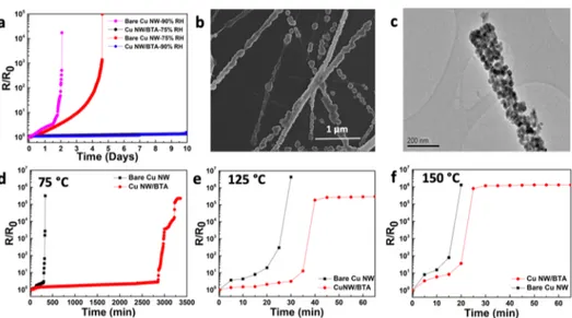
Oxidation Resistance of Networks under Ambient Conditions. To compare the oxidation resistance perform-ance under ambient conditions, sheet resistperform-ances of bare Cu NW and BTA-passivated Cu NW networks were monitored for an extended period of time (i.e., 1 year). Networks were prepared with similar NW densities of 124−148 mg/m2 to
eliminate the effect of the NW density on the degradation of electrodes. During measurements, all electrodes were kept under atmospherically regulated conditions (i.e., in air with an average temperature of 22± 2 °C and average humidity of 25 ± 5% RH). The normalized sheet resistancethe ratio of the sheet resistance to the initial sheet resistance (R/R0)was used as a test standard. Figure 2a shows the graph of
normalized sheet resistance versus time for bare and BTA-passivated Cu NW networks. Bare Cu NWs lost their conductivity within 12 days, while the sheet resistance of BTA-passivated networks increased by a factor of only 1.1 at the end of one year. Scanning electron microscopy (SEM) images of bare and BTA-passivated Cu NW networks after a
electrodes were monitored via conductivity measurements and XPS and transmission electron microscopy (TEM) analyses. Networks prepared for these studies had similar NW densities of 148−162 mg/m2. Increased humidity severely affected the
stability of bare Cu NW networks. Although bare Cu NW networks lost their electrical conductivity due to oxidation in 12 days under ambient conditions, it took approximately 5 days for the complete loss of conductivity under 75% RH
(Figure 3a). The corrosion rate was much higher under 90%
RH for bare Cu NW networks so that they became nonconducting only after 2 days (Figure 3a). In sharp contrast, the resistance change for BTA-passivated Cu NW networks was negligible at the end of 10 days. The chemical composition of NWs after exposure to high humidity conditions was determined through XPS analysis. Characteristic strong satellite peaks appearing at 942.5 and 962.2 eV, as well as Cu 2p3/2 and Cu 2p1/2 peaks at 933.3 and 953.1 eV,
respectively, in the XPS spectrum revealed that the bare Cu NWs were oxidized predominantly to CuO with a minor contribution from Cu2O32(Figure S5). SEM and TEM images provided in Figure 3b,c, respectively, reveal nanoparticle formation on the surface of the bare Cu NWs upon exposure to high humidity conditions. Since the polycrystalline oxide layer forms throughout the surface of NWs, the formed grain boundaries and other types of defects act as nucleation sites for the formation of CuO/Cu2O nanoparticles.36
Oxidation Resistance of Networks at Elevated Temperatures. Since typical optoelectronic device fabrication processes involve multiple annealing steps, Cu NW networks should be thermally stable at these elevated temperatures. To compare the thermal stability of bare and BTA-passivated Cu NW networks, samples were calcined at 75, 125, and 150°C in air. The average initial sheet resistance of these Cu NW networks was 19 ± 3.8 Ω/sq, while the initial areal mass density of networks was in the range of 120−150 mg/m2. For all thermal aging tests, samples were directly exposed to the chosen temperatures in air without a heating ramp.Figure 3d− f shows the change in the sheet resistance for both bare and BTA-passivated Cu NW networks as a function of the time at calcination temperatures of 75, 125, and 150°C, respectively. At 75°C, BTA-passivated networks showed superior stability with respect to the bare networks (Figure 3d). Although it took approximately 250 min for the bare Cu NW network to be totally nonconductive at 75 °C, similar failure occurred within 50 min at 125°C and only within 20 min at 150 °C. On the other hand, BTA-passivated Cu NW networks showed better resistance against oxidation compared to the bare Cu
Figure 2. (a) Change in the sheet resistance of bare and BTA-passivated Cu NW networks under ambient conditions. SEM images of (b) bare Cu NW networks and (c) BTA-passivated Cu NW networks after one-year exposure to ambient conditions.
NW samples (Figure 3e,f). Typical annealing temperatures involved in the fabrication of optoelectronic devices lie around 100 °C, and hence, BTA-passivated Cu NW networks will survive these processes. Moreover, the rate of change in resistance values decreased significantly before networks became completely insulating for all of the calcination temperatures investigated (Figure 3d−f). This very slow rate could be attributed to the gradual loss of BTA following the rapid loss at the initial stage.37
To determine the oxidation states of both bare and BTA-passivated Cu NW networks, XPS analysis was performed
following 5 min calcination at 75, 125, and 150 °C. Three major factors may tend to change the oxidation state of Cu in the presence of atmospheric oxygen and thermal activation provided by calcination/heat. Firstly, atmospheric O2can be
activated and dissociated on the Cu surface, leading to the oxidation of Cu. This was observed for the freshly prepared bare Cu NW networks at 25°C (Figure 4b), where the surface of the Cu NWs was determined to be oxidized to predominantly Cu2+ (i.e., CuO) species with a smaller contribution from Cu+ (i.e., Cu2O) species. Oxidation of
metallic Cu to Cu2+ and Cu+ is clearly discernible by the
Figure 3.(a) Change in the sheet resistance of bare and BTA-passivated Cu NW networks kept at 75 and 90% RH for 10 days. (b) SEM and (c) TEM images of bare Cu NW networks aged under 75± 5% RH. Change in the sheet resistance of bare Cu NW and BTA-passivated Cu NW networks as a function of the calcination time in air at (d) 75, (e) 125, and (f) 150°C (lines are for visual aid).
Figure 4.(a−c) Cu 2p XPS spectra of bare and BTA-passivated Cu NW networks at 25 °C and compared with networks calcined at 75, 125, and 150°C. (d) Attenuated total reflection-infrared (ATR-IR) data obtained after 5 min calcination of BTA-passivated Cu NW networks in air within 25−150 °C. (e) ATR-IR spectra obtained for BTA-passivated Cu NWs at 25 °C (black spectrum), after degradation of the BTA coating at 250 °C (red spectrum) and bare Cu NWs (blue spectrum) at 25°C.
where at 25°C, the bare Cu NW surface is dominated by CuO with a minor contribution from Cu2O (note the minor 945.1 eV Cu2O satellite feature at 25°C). However, upon calcination
at 75°C, a partial reduction was observed and bare Cu NWs tend to reveal mostly Cu2O species, evident by the loss of the
high B.E. Cu 2p3/2shoulder at 934.0 eV, sharpening of the Cu 2p3/2signal, a decrease in the 943.3 eV CuO satellite feature,
and strengthening of the 946.1 eV Cu2O satellite feature
(Figure 4b). Upon calcination at a higher temperature of 125
°C, Cu2O was reoxidized to CuO, which was readily visible
through the reappearance of the 934.0 eV Cu 2p3/2shoulder and 943.3 eV satellite feature. Further calcination at 150 °C tended to partially reduce the Cu NWs back to mostly Cu2O (see the satellite inFigure 4b). These oxidation state variations of bare Cu NW network as a function of temperature was also in accordance with the surface atomic oxygen content determined via XPS measurements (seeFigure S6a).
When Cu NWs were passivated with BTA, Cu sites tend to protect their metallic nature in air for all investigated temperatures (25−150 °C) (Figure 4a−c). The lack of a significant amount of CuO was evident due to the Cu 2p3/2
B.E. located at 931.9 eV and the absence of a high B.E. shoulder at 934.0 eV.32The presence of a significant amount of Cu2O could also be readily ruled out by considering the lack of
a satellite peak at 944 eV and more importantly by considering the minuscule concentration of surface atomic oxygen (ca. 2%) determined by XPS (Figure S6b). It is obvious that BTA provided an excellent oxidation resistance for metallic Cu sites within 25−150 °C in air for moderate time periods.
To demonstrate the thermal stability of BTA on Cu NW networks, passivated networks were monitored through ATR-IR spectroscopy upon 5 min calcination within a temperature range of 25−250 °C.Figure 4d shows that the BTA overlayer remains intact after calcination in air up to 125°C, while it drastically decomposes after calcination at 150°C.
Detailed ATR data for the BTA-passivated Cu NW networks calcined at 25 °C (black spectrum in Figure 4e) are in very good agreement with the former studies.32It was apparent that after calcination at 150 °C, most of the vibrational features either disappear completely or significantly attenuate in intensity. ATR-IR spectra after calcination within 150−250 °C were almost identical, suggesting that following the drastic transformation at T ≥ 150 °C, the vibrational structure was starkly modified, but this modified structure remained rather intact at temperatures above 150 °C. The ATR-IR spectrum obtained after calcination at 250 °C (red spectrum inFigure 4e) revealed two major modes that can survive upon
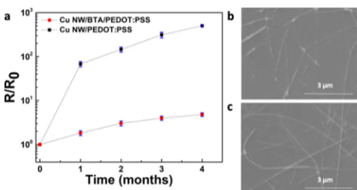
transparent layer, transport electrodes are generally in contact with a PEDOT:PSS layer in organic-based optoelectronic devices. Most of the PEDOT:PSS types used in optoelectronic devices have relatively high acidity (pH ∼ 3−4). Thus, the acidic nature of PEDOT:PSS eventually deteriorates the NW networks by acidic corrosion.41,42 As a result, long-term chemical corrosion stability against the acidic nature of PEDOT:PSS is another crucial requirement in industrial applications of transparent conducting electrodes. In this study, bare and BTA-passivated Cu NW networks were spin-coated with a 50 nm thick PEDOT:PSS (pH∼ 3) layer. Then, the stability of both bare Cu NW/PEDOT:PSS and Cu NW/ BTA/PEDOT:PSS samples was monitored through sheet resistance measurements for 4 months. PEDOT:PSS is well known to be sensitive to air exposure, and its electrical conductivity degrades in time due to the absorption of atmospheric water/oxygen. Therefore, all samples were kept in a glovebox under a controlled argon atmosphere (O2level <0.1
ppm, H2O level <0.1 ppm) throughout the test period to assure that the change in resistance was not related to the degradation of PEDOT:PSS. The initial average resistances for Cu NW/PEDOT:PSS samples and Cu NW/BTA/PE-DOT:PSS samples were measured as 27 ± 4 and 25 ± 2, Ω/sq, respectively. At the end of 4 months, the resistance of Cu NW/PEDOT:PSS samples increased by approximately 500 times, while the resistance of Cu NW/BTA/PEDOT:PSS samples increased by only 5 times (Figure 5a). It should also be noted that the maximum resistance of Cu NW/BTA/ PEDOT:PSS samples at the end of 4 months was below 150
Figure 5. (a) Change in the sheet resistance of bare Cu NW/ PEDOT:PSS and Cu NW/BTA/PEDOT:PSS networks with time (lines are for visual aid). SEM images of (b) bare Cu NW/ PEDOT:PSS network and (c) Cu NW/BTA/PEDOT:PSS network after 4 months.
Ω/sq, which is still low enough for many optoelectronic applications. The obtained results were also supported by SEM analysis. The SEM image of the bare Cu NW/PEDOT:PSS sample showed that the structural integrity of the network was lost due to severe etching of the NWs (Figure 5b). Due to the acidic nature of PEDOT:PSS, bare Cu NWs were dissolved and ruptured within this acidic polymeric media. The overall electrical percolation within the network was destroyed, confirming the sheet resistance measurements. On the other hand, no morphological changes were observed for the Cu NW/BTA/PEDOT:PSS samples (Figure 5c). This implies that BTA-passivated samples show superior resistance against corrosion. The BTA layer deposited by a simple, solution-based method suppresses the corrosion rate of Cu NWs under acidic conditions. These results are in perfect agreement with previous studies, where BTA treatment was shown to decrease the acidic corrosion rate of bulk Cu.43
BTA-Passivated Cu NW-Based Capacitive Tactile Sensors. Transparent,flexible, capacitive tactile sensors were fabricated to demonstrate the potential of BTA-passivated Cu NW networks in optoelectronic device applications. Sensors were used to map the pressure applied by fingers and other objects with various shapes. Figures 6a−c shows the photo-graphs of the fabricated 5 × 5 matrix, single-electrode capacitive sensor devices.
For this capacitive sensor, in the loading mode, only one electrode was used to both transmit and receive signals. Electrodes were loaded capacitively by a conductive object and formed a displacement current flow through a conductive object to the ground. Bringing the conductive object closer to the sensor caused an increase in the capacitive coupling between the conductive object and the corresponding electrode. Changes in the magnitude of the output capacitance were proportional to the applied pressure. Figure S7 shows
that the output capacitance of the fabricated sensors changes linearly with the applied pressure, where the sensitivity of the sensors was determined as 0.6× 10⁻³μF/kPa. An increase in the applied pressure decreased the thickness of the thermo-plastic polyurethane (TPU) layer and increased the capacitance. The capacitance changes of 25 electrodes were recorded as a mappingfigure.Figure 6c,f showed an L-shaped conductive object (aluminum foil in this case) that was placed on the device and the corresponding response on the capacitance map, respectively. Contact (touch) information, position, and applied relative pressure offingers or conductive objects interacting with the device could be obtained through the analysis of the increments in capacitance via mapping figures. As shown inFigure 6d, touching the tactile sensor with three fingers results in different capacitance values ranging from 0.15 to 0.17μF.
The fabricated device was also capable of preserving its functionality under bending conditions. Figure 6b shows the photo of the flexible sensor matrix attached to a transparent tube. Upon application of pressure to the sensor surface at three different points, similar and consistent map figures to those for the flat condition were obtained. Lower output capacitance values compared to that of the flat sensor were related to the incomplete coverage of the electrode area by fingers due to the curvature in the bent condition. It is worth noting that the control devices fabricated using bare Cu nanowire networks stopped working only 3 days after production. This signifies the necessity of the use of BTA for protecting these devices.
■
CONCLUSIONSIn summary, a simple, all-solution-based, and highly effective method to improve the resistance of Cu NW networks against oxidation was demonstrated. In this method, bulk Cu
Figure 6.Photographs of the (a) fabricated transparent capacitive tactile sensor, (b) sensor upon three-finger touch when bent, and (c) sensor when an“L”-shaped conductive object is placed above. (d) Capacitance maps upon three-finger touch when the sensor was flat. (e) Capacitance map of (b). (f) Capacitance map of (c).
NW networks are not limited to tactile sensors, and they can be used in a wide range of different optoelectronic applications. The results obtained in the current study are of referring significance, as they provide a simple and scalable means to fabricate affordable Cu NW networks with high optoelectronic performance and excellent stability that can be utilized as promising alternatives to existing conventional materials used in optoelectronic devices.
■
EXPERIMENTAL SECTIONChemicals. Hexadecylamine (HDA) (C16H35N,≥94.0% (a/a)),
copper (II) chloride dihydrate (CuCl2·2H2O,≥99.0%),D-(+)-glucose
monohydrate (anhydrous, 97.5−102.0%), poly(vinylpyrrolidone) (PVP) (MW= 55 000, monomer-based calculation), benzotriazole (BTA) (C6H5N3≥99.0%), chloroform (CHCl3, 99.8%), andDL-lactic
acid (90%) were purchased from Sigma-Aldrich and used as received. Poly(3,4-ethylenedioxythiophene)-poly(styrenesulfonate) (PE-DOT:PSS) with pH∼3 was purchased from Heraeus (Heraeus VP Al 4083).
Synthesis of Cu NWs. Cu NWs were synthesized according to a previously reported procedure developed by Mohl et al. with slight modifications.44In a typical synthesis, 147 mg of CuCl
2.2H2O, 350
mg of glucose, 1260 mg of HDA, and 70 mL of deionized (DI) water (18.3 MΩ) were mixed in a glass beaker and stirred for 12 h via vigorous magnetic stirring at room temperature to obtain a homogeneous mixture. Afterward, the obtained light blue emulsion was transferred to a Teflon-lined autoclave with 100 mL capacity. The reactor was sealed and heated at 105 °C for 12 h without further stirring. Following synthesis, the NWs were purified by centrifugation and washed repeatedly with DI water and ethanol. Next, a multiphase separation method was carried out to eliminate the byproducts and to get rid of excess HDA.45 Following purification, the product was dispersed within a 2 wt % PVP−ethanol solution. Excess PVP was removed by washing the NWs with ethanol. Thefinal product was then dispersed in ethanol for further processing.
Fabrication and Passivation of Transparent Conducting Electrodes. Ethanolic suspensions of Cu NWs were deposited onto soda lime silica glass and poly(ethylene terephthalate) (PET) substrates using spray coating. Cu NW dispersion was sprayed onto the substrates at 100°C using an airbrush fed by pure nitrogen gas at 1.5 atm. Following deposition, Cu NW networks on glass were annealed under vacuum at 200°C for 20 min to get rid of the residual PVP layer and to improve the electrical contact at junctions of Cu NWs. Electrodes on PET were immersed into a lactic acid−ethanol solution at a volume ratio of 1:20, which was followed by an ethanol rinse and drying. In the meantime, a 3 wt % BTA−ethanol solution was prepared by stirring at 300 rpm for 10 min in a tightly sealed glass vial at room temperature. The solution was then spin-coated onto Cu NW networks at a speed of 3000 rpm for 30 s after which the samples were dried at 70°C for 30 min. After 24 h, the samples were rinsed with ethanol to get rid of any excess BTA.
analyzers. Binding energy (B.E.) calibration was made by setting the adventitious carbon (C 1s) signal to 284.4 eV. Peakfitting, baseline correction, and deconvolution analysis of the XPS data were performed via CASA and OriginPro software. ATR-IR measurements were performed on a Bruker Alpha spectrometer equipped with a Bruker ATR attachment and a DLaTGS detector. Each ATR-IR spectrum was acquired with a frequency resolution of 4 cm−1 by averaging 32 scans. To eliminate atmospheric water and carbon dioxide vibrational signatures, a background spectrum of air was acquired before each sample spectrum.
Sheet resistance and transparency measurements were performed using a Keithley 2400 source meter and an Agilent 8453 UV−vis spectrophotometer, respectively. Continuous humidity and temper-ature measurements were performed with a chamber-mounted remote Weather Forecast digital hygrometer probe (temperature range =∼0 to +50°C, thermometer accuracy = ±1 °C, humidity range = 20− 98% RH, humidity accuracy =±5%).
■
ASSOCIATED CONTENT*
sı Supporting InformationThe Supporting Information is available free of charge at
https://pubs.acs.org/doi/10.1021/acsami.0c11729.
Scanning Electron Microscope (SEM) images, statistical information (diameter and length distribution histo-grams of nanowires), additional X-ray photoelectron spectroscopy (XPS) results, areal mass density (amd) calculation procedure, and graph related to the tactile sensor capacitance change with respect to pressure (PDF)
■
AUTHOR INFORMATIONCorresponding Author
Husnu Emrah Unalan− Department of Metallurgical and Materials Engineering, Department of Micro and
Nanotechnology, and Centre for Solar Energy Research and Applications (GÜNAM), Middle East Technical University, Ankara 06800, Turkey; orcid.org/0000-0003-3667-179X; Email:[email protected]
Authors
Sevim Polat Genlik− Department of Materials Science and Engineering, Ohio State University, Columbus, Ohio 43210, United States
Dogancan Tigan− Department of Metallurgical and Materials Engineering, Middle East Technical University, Ankara 06800, Turkey
Yusuf Kocak− Department of Chemistry, Bilkent University, Ankara 06800, Turkey; orcid.org/0000-0003-4511-1321
Kerem Emre Ercan− Department of Chemistry, Bilkent University, Ankara 06800, Turkey; orcid.org/0000-0003-4650-7977
Melih Ogeday Cicek− Department of Metallurgical and Materials Engineering, Middle East Technical University, Ankara 06800, Turkey
Sensu Tunca− Department of Metallurgical and Materials Engineering, Middle East Technical University, Ankara 06800, Turkey
Serkan Koylan− Department of Metallurgical and Materials Engineering, Middle East Technical University, Ankara 06800, Turkey
Sahin Coskun− Department of Metallurgical and Materials Engineering, Eskisehir Osmangazi University, Eskisehir 26040, Turkey
Emrah Ozensoy− Department of Chemistry and UNAM National Nanotechnology Center, Bilkent University, Ankara 06800, Turkey; orcid.org/0000-0003-4352-3824
Complete contact information is available at:
https://pubs.acs.org/10.1021/acsami.0c11729 Author Contributions
H.E.U. and E.O. supervised the research. S.P.G. and D.T. planned and performed the experiments. S.P.G. collected and analyzed the data and wrote the paper. Y.K. and K.E.E. helped with characterization and discussed the data. M.O.C., S.T., and S.K. performed the experiments to show the functionality of the discussed material. S.C. provided scientific discussions to give direction to the research. All authors have discussed, commented on, and revised the manuscript.
Notes
The authors declare no competingfinancial interest.
■
ACKNOWLEDGMENTSThis work was financially supported by the Middle East Technical University through the Scientific Research Projects Programme under project numbers BAP-07-02-2016-003, BAP-07-02-2017-011, and BAP-07-02-2017-004-265. E.O. acknowledges the scientific collaboration with the TARLA project founded by the Ministry of Development of Turkey (project code DPT2006K-120470). The authors also acknowl-edge Mr. Mete Duman (UNAMNational Nanotechnology Center, Ankara, Turkey) for the design and production of technical schematics.
■
REFERENCES(1) Bellet, D.; Lagrange, M.; Sannicolo, T.; Aghazadehchors, S.; Nguyen, V. H.; Langley, D. P.; Munoz-Rojas, D.; Jimenez, C.; Brechet, Y.; Nguyen, N. D. Transparent Electrodes Based on Silver Nanowire Networks: From Physical Considerations Towards Device Integration. Materials 2017, 10, 570.
(2) Hosono, Hideo.; David, C. P. Handbook of Transparent Conductors; Springer Science & Business Media, 2010.
(3) Coskun, S.; Ates, E. S.; Unalan, H. E. Optimization of Silver Nanowire Networks for Polymer Light Emitting Diode Electrodes. Nanotechnology 2013, 24, No. 125202.
(4) Ye, S.; Rathmell, A. R.; Chen, Z.; Stewart, I. E.; Wiley, B. J. Metal Nanowire Networks: The Next Generation of Transparent Con-ductors. Adv. Mater. 2014, 26, 6670−6687.
(5) Sannicolo, T.; Lagrange, M.; Cabos, A.; Celle, C.; Simonato, J. P.; Bellet, D. Metallic Nanowire-Based Transparent Electrodes for Next Generation Flexible Devices: a Review. Small 2016, 12, 6052− 6075.
(6) Kumar, A.; Zhou, C. The Race To Replace Tin-Doped Indium. ACS Nano 2010, 4, 11−14.
(7) Niu, Z.; Cui, F.; Yu, Y.; Becknell, N.; Sun, Y.; Khanarian, G.; Kim, D.; Dou, L.; Dehestani, A.; Schierle-Arndt, K.; Yang, P. Ultrathin Epitaxial Cu@Au Core-Shell Nanowires for Stable Transparent Conductors. J. Am. Chem. Soc. 2017, 139, 7348−7354.
(8) Stewart, I. E.; Rathmell, A. R.; Yan, L.; Ye, S.; Flowers, P. F.; You, W.; Wiley, B. J. Solution-Processed Copper-Nickel Nanowire Anodes for Organic Solar Cells. Nanoscale 2014, 6, 5980−5988.
(9) Won, Y.; Kim, A.; Lee, D.; Yang, W.; Woo, K.; Jeong, S.; Moon, J. Annealing-Free Fabrication of Highly Oxidation-Resistive Copper Nanowire Composite Conductors for Photovoltaics. NPG Asia Mater. 2016, 6, No. e105.
(10) Chen, J.; Zhou, W.; Chen, J.; Fan, Y.; Zhang, Z.; Huang, Z.; Feng, X.; Mi, B.; Ma, Y.; Huang, W. Solution-Processed Copper Nanowire Flexible Transparent Electrodes with PEDOT:PSS as Binder, Protector and Oxide-Layer Scavenger for Polymer Solar Cells. Nano Res. 2015, 8, 1017−1025.
(11) Im, H. G.; Jung, S. H.; Jin, J.; Lee, J.; Lee, D.; Lee, J. Y.; Kim, I. D.; Bae, B. S.; Lee, D. Flexible Transparent Conducting Hybrid Film Using a Surface-Embedded Copper Nanowire Network: A Highly Oxidation-Resistant Copper Nanowire Electrode for Flexible Optoelectronics. ACS Nano 2014, 8, 10973−10979.
(12) Song, J.; Li, J.; Xu, J.; Zeng, H. Superstable Transparent Conductive Cu@Cu4Ni Nanowire Elastomer Composites Against
Oxidation, Bending, Stretching, and Twisting for Flexible and Stretchable Optoelectronics. Nano Lett. 2014, 14, 6298−6305.
(13) Wang, J.; Chen, H.; Zhao, Y.; Zhong, Z.; Tang, Y.; Liu, G.; Kang, J.; et al. Programmed Ultrafast Scan Welding of Cu Nanowires Network with Pulsed Ultraviolet Laser Beam for Transparent Conductive Electrodes and Flexible Circuits. ACS Appl. Mater. Interfaces 2020, 12, 35211−35221.
(14) Chu, H. C.; Chang, Y. C.; Lin, Y.; Chang, S. H.; Chang, W. C.; Li, G. A.; Tuan, H. Y. Spray-Deposited Large-Area Copper Nanowire Transparent Conductive Electrodes and Their Uses for Touch Screen Applications. ACS Appl. Mater. Interfaces 2016, 8, 13009−13017.
(15) Bao, C.; Yang, J.; Gao, H.; Li, F.; Yao, Y.; Yang, B.; Fu, G.; Zhou, X.; Yu, T.; Qin, Y.; Liu, J.; Zou, Z. In Situ Fabrication of Highly Conductive Metal Nanowire Networks with High Transmittance From Deep-Ultraviolet to Near-Infrared. ACS Nano 2015, 9, 2502− 2509.
(16) Celle, C.; Cabos, A.; Fontecave, T.; Laguitton, B.; Benayard, A.; Guettaz, L.; Pelissier, N.; Nguyen, V. H.; Bellet, D.; Munoz-Rojas, D.; Simonato, J. P. Oxidation of Copper Nanowire Based Transparent Electrodes in Ambient Conditions and Their Stabilization by Encapsulation: Application to Transparent Film Heaters. Nano-technology 2018, 29, No. 085701.
(17) Zhai, H.; Wang, R.; Wang, X.; Cheng, Y.; Shi, L.; Sun, J. Transparent Heaters Based on Highly Stable Cu Nanowire Films. Nano Res. 2016, 9, 3924−3936.
(18) Stewart, I. E.; Ye, S.; Chen, Z.; Flowers, P. F.; Wiley, B. J. Synthesis of Cu-Ag, Cu-Au, and Cu-Pt Core-Shell Nanowires and Their Use in Transparent Conducting Films. Chem. Mater. 2015, 27, 7788−7794.
(19) Rathmell, A. R.; Nguyen, M.; Chi, M.; Wiley, B. J. Synthesis of Oxidation-Resistant Cupronickel Nanowires for Transparent Con-ducting Nanowire Networks. Nano Lett. 2012, 12, 3193−3199.
(20) Chen, J.; Chen, J.; Li, Y.; Zhou, W.; Feng, X.; Huang, Q.; Zheng, J.; Liu, R.; Ma, Y.; Huang, W. Enhanced Oxidation-resistant Cu−Ni Core−Shell Nanowires: Controllable One-Pot Synthesis and Solution Processing to Transparent Flexible Heaters. Nanoscale 2015, 7, 16874−16879.
(21) Hsu, P. C.; Wu, H.; Carney, T. J.; McDowell, M. T.; Yang, Y.; Garnett, E. C.; Li, M.; Hu, L.; Cui, Y. Passivation Coating on Electrospun Copper Nanofibers for Stable Transparent Electrodes. ACS Nano 2012, 6, 5150−5156.
(22) Chen, Z.; Ye, S.; Stewart, I. E.; Wiley, B. J. Copper Nanowire Networks with Transparent Oxide Shells That Prevent Oxidation without Reducing Transmittance. ACS Nano 2014, 8, 9673−9679.
Arabian J. Chem. 2020, 13, 481−544.
(28) Brusic, V.; et al. Copper Corrosion With and Without Inhibitors. J. Electrochem. Soc. 1991, 138, No. 2253.
(29) Cotton, J. B.; Scholes, I. R. Benzotriazole and Related’ Compounds As. Brit. Corros. J. 1967, 2, 1−5.
(30) Xue, G.; Ding, J. Chemisorption of a Compact Polymeric Coating on Copper Surfaces From a Benzotriazole Solution. Appl. Surf. Sci. 1990, 40, 327−332.
(31) Chadwick, D.; Hashemi, T. Adsorbed Corrosion Inhibitors Studied by Electron Spectroscopy: Benzotriazole on Copper and Copper Alloys. Corros. Sci. 1978, 18, 39−51.
(32) Jiang, P.; Prendergast, D.; Borondics, F.; Porsgaard, S.; Giovanetti, L.; Pach, E.; Salmeron, M.; et al. Experimental and Theoretical Investigation of the Electronic Structure of Cu2O and
CuO Thin Films on Cu (110) Using X-ray Photoelectron and Absorption Spectroscopy. J. Chem. Phys. 2013, 138, No. 024704.
(33) Susman, M. D.; Feldman, Y.; Vaskevich, A.; Rubinstein, I. Chemical Deposition and Stabilization of Plasmonic Copper Nano-particle Films on Transparent Substrates. Chem. Mater. 2012, 24, 2501−2508.
(34) Stewart, I. E. The Impact of Morphology and Composition on the Resistivity and Oxidation Resistance of Metal Nanostructure Films. PhD Thesis, Duke University, 2016.
(35) Popova, I.; Yates, J. T. Adsorption and Thermal Behavior of Benzotriazole Chemisorbed onγ-Al2O3. Langmuir 1997, 13, 6169−
6175.
(36) Hajimammadov, R.; Mohl, M.; Kordas, K. Native Oxide Formation on Pentagonal Copper Nanowires: A TEM Study. Surf. Sci. 2018, 672−673, 19−22.
(37) Christensen, T. M.; Sorensen, N. R. Thermal Stability of Benzotriazole on Copper During Atmospheric Corrosion. Surf. Interface Anal. 1991, 17, 3−6.
(38) Liu, D.; Yang, S.; Lee, S. T. Preparation of Novel Cuprous Oxide− Fullerene [60] Core− Shell Nanowires and Nanoparticles via a Copper (I)-Assisted Fullerene-Polymerization Reaction. The. J. Phys. Chem. C 2008, 112, 7110−7118.
(39) Tammer, M.; Sokrates, G. Infrared and Raman Characteristic Group Frequencies: Tables and Charts; John Wiley & Sons, 2004.
(40) Akgul, F. A.; Akgul, G.; Yildirim, N.; Unalan, H. E.; Turan, R. Influence of Thermal Annealing on Microstructural, Morphological, Optical Properties and Surface Electronic Structure of Copper Oxide Thin Films. Mater. Chem. Phys. 2014, 147, 987−995.
(41) Song, T. B.; Rim, Y. S.; Liu, F.; Bob, B.; Le, S.; Hsieh, Y. T.; Yang, Y. Highly Robust Silver Nanowire Network for Transparent Electrode. ACS Appl. Mater. Interfaces 2015, 7, 24601−24607.
(42) Choi, D. Y.; Kang, H. W.; Sung, H. J.; Kim, S. S. Annealing-Free, Flexible Silver Nanowire−Polymer Composite Electrodes via a Continuous Two-Step Spray-Coating Method. Nanoscale 2013, 5, 977−983.
(43) Ullah, S.; Shariff, A. M.; Bustam, M. A.; Nadeem, M.; Naz, M. Y.; Ayoub, M. Study on Effect of Benzotriazole and Surfactants on