LIQUID
a thesis
submitted to the department of physics
and the institute of engineering and science
of bilkent university
in partial fulfillment of the requirements
for the degree of
master of science
By
Mustafa Karak¨ose
September, 2003
Assoc. Prof. Dr. Ahmet Oral (Supervisor)
I certify that I have read this thesis and that in my opinion it is fully adequate, in scope and in quality, as a thesis for the degree of Master of Science.
Assoc. Prof. Dr. Recai M. Ellialtıo˘glu
I certify that I have read this thesis and that in my opinion it is fully adequate, in scope and in quality, as a thesis for the degree of Master of Science.
Asst. Prof. Dr. D¨on¨u¸s Tuncel
Approved for the Institute of Engineering and Science:
Prof. Dr. Mehmet Baray
Director of the Institute of Engineering and Science
MICROSCOPE OPERATING IN AIR AND LIQUID
Mustafa Karak¨ose M.S. in Physics
Supervisor: Assoc. Prof. Dr. Ahmet Oral September, 2003
In this thesis, a new atomic force microscope capable of measuring in liquid and air has been introduced. The highly improved design of the instrument elim-inates some of the technical problems which are occurred before. The instrument makes use of the small amplitude AC-Mode technique to detect the interaction forces between the tip and the surface. Some results of initial test scans of the instrument are displayed.
Keywords: Scanning Tunnelling Microscopy, Atomic Force Microscopy, Fiber In-terferometry, Low Amplitude AC Mode AFM.
SIVIDA VE HAVADA C
¸ ALIS
¸AN B˙IR ATOM˙IK
KUVVET M˙IKROSKOBUNUN YAPIMI
Mustafa Karak¨ose Fizik, Y¨uksek Lisans
Tez Y¨oneticisi: Do¸c. Dr. Ahmet Oral Eyl¨ul, 2003
Bu tezde, sıvı ve havada ¸calı¸sabilen yeni bir atomik kuvvet mikroskobu tanıtıldı. Aletin ¸cok geli¸smi¸s tasarımı daha ¨once ortaya ¸cıkmı¸s bazı teknik sorun-ları ortadan kaldırdı. Alet y¨uzey ve u¸c arasındaki kuvvet etkile¸simlerini belir-lemek i¸cin d¨u¸s¨uk genlikli alternatif akım tekniˇgini kullanmaktadır. Bazı deneme taramalarının sonu¸clari g¨osterilmi¸stir.
Anahtar s¨ozc¨ukler : Taramalı T¨unelleme Mikroskobisi, Atomik Kuvvet Mikroskopisi, Fiber ˙Interferometresi, D¨u¸s¨uk Genlikli Alternatif Akım Modunda AKM.
I would like to express my deep gratitude to my supervisor Assoc. Prof. Dr. Ahmet Oral, for his friendly attitude and guidance. He saw the light at the end of the tunnel before me and turned me to the light. This work would never be done without him.
I debt special thanks to Mehrdad Atabak and Koray ¨Urkmen for their adamantine faith and patience. When I needed help, they were always ready to help.
The friendly ambience in the laboratory refreshes me and cheered me up to carry on, so I have to thank all of the other friends in the laboratory: G¨oksel Durkaya, M¨unir Dede, G¨ozde Bayer and Serdar ¨Ozdemir.
1 Introduction 1
1.1 Scanning Tunnelling Microscopy(STM) . . . 2
1.2 Atomic Force Microscopy(AFM) . . . 5
1.3 Motivation behind the Force Measurement in Liquids . . . 9
1.4 Force Measurement Techniques . . . 10
1.4.1 Vacuum Tunneling . . . 10
1.4.2 Mechanical Resonance . . . 11
1.4.3 Optical Interferometry . . . 11
1.4.4 Optical Beam Deflection . . . 11
1.5 AFM Operation Modes . . . 12
1.5.1 The DC Method . . . 12
1.5.2 Large Amplitude AC Method . . . 13
1.5.3 Small Amplitude AC Method . . . 13
2 Experimental Setup 14
2.1 Overview of the Instrument . . . 14
2.1.1 The Sample Slider . . . 15
2.1.2 The Fiber Slider . . . 18
2.1.3 The Cantilever Assembly . . . 19
2.1.4 The Tunneling Tip Assembly . . . 22
2.2 Cantilever and Tip Preparation . . . 22
2.3 The Interferometer . . . 23
2.4 The Control Units . . . 26
2.4.1 The Electronics Control Unit . . . 26
2.4.2 The Software: SPM . . . 27
1.1 The quantum mechanical electron tunnelling phenomenon. . . 2
1.2 The region of interaction in AFM. . . 6
1.3 Interatomic forces vs the separation between the tip and the surface. 7 2.1 A general view of the liquid-air AFM. . . 15
2.2 The vertical and lateral sample slider. . . 16
2.3 The principle of shear piezoelectric slider . . . 17
2.4 The x-z fiber slider and fiber piezo. . . 20
2.5 The cantilever assembly. . . 21
2.6 The electrochemical etching setup. . . 23
2.7 The electrochemically etched AFM tip. . . 24
2.8 Schematic diagram of the optical interferometer. . . 25
2.9 The Electronics Control Unit . . . 29
3.1 STM-tip image of a 4×4 µm2 GaAs grating, Loop Gain: 999, Vertical Range: 2.87 µm, Scan speed: 1 µm/s, Tunneling Current: -0.32 nA, Bias voltage: -0.1 V . . . 32
3.2 The reverse scan of the above scan. . . 32 3.3 STM-tip image of a 4×4 µm2
GaAs grating, Loop Gain: 999, Vertical Range: 3.01 µm, Scan speed: 2 µm/s, Tunnelling Current: -0.35 nA, Bias voltage: -0.1 V . . . 33 3.4 The reverse scan of the above scan. . . 33 3.5 STM-tip image of a 4×4 µm2
GaAs grating, Loop Gain: 999, Vertical Range: 3 µm, Scan speed: 3 µm/s, Tunneling Current: -0.32 nA, Bias voltage: -0.1 V . . . 34 3.6 The reverse scan of the above scan. . . 34 3.7 STM-tip image of a 4×4 µm2
GaAs grating, Loop Gain: 999, Vertical Range: 4.8 µm, Scan speed: 1 µm/s, Tunneling Current: -0.4 nA, Bias voltage: -0.1 V . . . 35 3.8 The reverse scan of the above scan. . . 35 3.9 STM-tip image of a 4×4 µm2
GaAs grating, Loop Gain: 999, Vertical Range: 2.72 µm, Scan speed: 1µm/s, Tunneling Current: -0.4 nA, Bias voltage: -0.1 V . . . 36 3.10 The reverse scan of the above scan. . . 36 3.11 AFM-tip image of a hexagonal GaAs grating, Loop Gain: 999,
Vertical Range: 1.2 µm, Scan speed: 1 µm/s, Tunneling Current: -1.61 nA, Bias voltage: -0.5 V . . . 37 3.12 The reverse scan of the above scan. . . 37 3.13 AFM-tip image of a rectangular GaAs grating, Loop Gain: 999,
Vertical Range: 2.85 µm, Scan speed: 0.5 µm/s, Tunneling Cur-rent: -0.95 nA, Bias voltage: -0.5 V . . . 38 3.14 The reverse scan of the above scan. . . 38
3.15 AFM-tip image of a hexagonal silicon grating, Loop Gain: 999, Vertical Range: 1.2 µm, Scan speed: 1 µm/s, Tunneling Current: -1.61 nA, Bias voltage: -0.5 V . . . 39
Introduction
Generally the answers to big questions lie in little things. Recently, there has been a growing interest in nanotechnology, which is concerned with the science and technology of scientific processes in nanometer scale. [1]
New tools are needed to manipulate the matter on the nanometer scale. In 1980 a new revolutionary method of microscopy known as Scanning Probe Mi-croscopy, SPM, has been introduced by Binnig and Rohrer [2], in which the basic component is a sharp tip which connects the macroscopic world and the enigmatic realm of nanometer scale. Since then, the applications have been increasing ex-ponentially in fields as diverse as surface physics, chemistry, tribology, biology and optics. As the technique becomes more widely available its use is spread-ing to even more diverse fields such as catalysis, micromechanics, and medical implant technology. SPM is also beginning to emerge as a useful and popular technique for research and development, quality control in several industries such as the semiconductor and big-technology industries. The reason for its nearly instantaneous acceptance as a characterization tool is that SPM provides three-dimensional, real space images of surfaces at high spatial resolution. When the sample is clean and flat, even atoms can be imaged. SPM also allows imaging of organic samples at unprecedented levels of resolution without harming them.
All probe microscopes have two common features: 1
A) A sharp, tiny probe gets very close to the sample and feels the surface by monitoring some kind of interaction, between the probe and the surface, which is very sensitive to distance.
B) The sample is scanned with near atomic accuracy and the variation in the interaction is translated to a topographic map of the surface.
1.1
Scanning Tunnelling Microscopy(STM)
The design of Binnig and Rohrer is based on electron tunnelling, which is the transition of an electron from a classically allowed region to another, which are separated by a potential barrier. This transition happens in STM from the sharp tip to the surface to be examined through an air gap.
Figure 1.1: The quantum mechanical electron tunnelling phenomenon.
The solution of Schrodinger’s Equation for a rectangular barrier in one di-mension [3] is given by:
ψ = exp(−kz) (1.1) k =q2m(V − E)/¯h (1.2) V is the barrier height, k is decay length and E is the energy of the electron. Tunnelling current [4] is proportional to the transmission probability T through the potential barrier of width a. The transmission probability can be estimated by the following equation:
T2
' exp(−2ka) (1.3) so we can say that the tunneling current
I ∝ exp(−ka) (1.4) In STM, a bias voltage is applied between the sharp tip and surface, which shifts the Fermi level of one side, so that the electrons can tunnel from the filled states side through the gap to the empty states side.
With the help of Bardeen’s formalism [5] Tersoff and Hamann [6] derived an expression for the tunneling current including the lateral variations of the potential barrier, which is caused by the atomic charge density of the surface:
I = 2πe ¯ h X µ,ν f (Eµ)(1 − f(Eν + eU ))|Mµν| 2 δ(Eµ− Eν) (1.5)
where F(E) is the Fermi function, Eµ and Eν are the energies of the states in
the absence of tunneling, Mµν is the tunneling matrix element between states Ψµ
of the metal probe tip and Ψν of the sample surface and U is the sample bias
voltage [7]. In equation 1.5 the only difficulty is to evaluate the tunneling matrix element Mµν. Bardeen [8] showed that
Mµν = ¯ h 2m Z d~S · (Ψ∗ µ5 Ψν− Ψν 5 Ψ∗µ) (1.6)
the integral is over any surface lying entirely within the barrier region. Neglecting the variation of the potential in the region of integration, we can say that
Ψ = Z d~qaqe−κqzei~q·~x (1.7) where κq = q κ2 + |~q|2 (1.8)
z is the height, q is the Fourier wavevector and aq is the corresponding expansion
coefficient.
Similarly, if we expand Ψ∗ replacing a
q with bq, z with zt-z and ~x with ~x − ~xt
and then substitute them into equation 1.6
Mµν = 4π2 ¯ h2 m Z d~qaqb∗qκqe−κqztei~q· ~xt (1.9)
Here ~xt and zt are the lateral and longitudinal components of the tip.
In the case of STM, if the sample bias voltage is small and the temperature is low enough, and if the tip is replaced by a point probe, equation 1.5 may be written as I ∝X ν |Ψ(~ r0)| 2 δ(Eν− EF) (1.10)
The right hand side of equation 1.10 is nothing but the surface local density of states (LDOS) at the Fermi level EF at the position of the tip ~r0. The theory
of Tersoff and Hamann predicts that the tip follows the contours of LDOS at EF during scanning. The estimated lateral resolution is roughly 2(R + ∆z)
1/2˚
where R is the tip radius and ∆z is the width of the potential barrier. Tersoff and Hamann model is commonly used in STM imaging but there is some limitations to the theory. The theory is valid only in the absence of significant tip sample interactions [7].
1.2
Atomic Force Microscopy(AFM)
After the invention of STM, the interaction between the tip and the surface turned out to be not so simple as it initially appeared. A simple theory predicts and exponential variation between the current I and separation s,
φb ≈ 0.95(
d(lnI) dz )
2
(1.11) where φb is the apparent barrier height [9]. This barrier height drops to zero at
small separations, which is much lower than the expected value. Coombs and Pethica [10] suggested that this unexpected effect was caused by a repulsive force between the tip and the surface, which in turn causes the modulation of the gap width to be smaller than the oscillatory motion applied. This causes the amplitude of current oscillations.
The realization of the existence of tip-surface forces makes the nanoscientists to find a way to measure them. The result was the invention of AFM [11]. The foremost advantage of AFM over STM is that it can be used over a wide range of samples, non-conducting ones as well as conducting ones. As a result of this, AFM technology grew rapidly. It is not uncommon to buy a commercial AFM, which is offered by a number of companies.
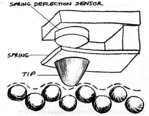
The operating principle of AFM is simple: A sharp tip integrated to a can-tilever spring is put to a very close distance to the surface and then scanned over the surface. The force interaction between the tip and the surface causes the cantilever spring to bend. The deflection of the cantilever is measured and this allows us to control the distance between the tip and the surface with a feedback
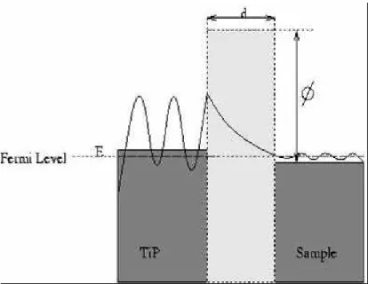
Figure 1.2: The region of interaction in AFM.
circuit.
All force microscopes have five essential components: ∗ A sharp tip integrated to a cantilever spring. ∗ A way of sensing cantilever deflection.
∗ A feedback system to monitor the deflection. ∗ A scanning system.
∗ A display system to convert the received data into an image [12]. Last three parts are used for STM too.
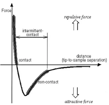
AFM can be operated in three modes: contact, non-contact and intermittent contact 1.3.
Figure 1.3: Interatomic forces vs the separation between the tip and the surface.
In contact mode, the tip is practically touching the surface while scanning the surface. At this very close proximity, the repulsive force between the tip and the surface deforms the tip and generally atomic resolution is not possible. The imaging force used to record atoms with the contact mode AFM is greater than 10−9 N. Ferrante and Smith [13] have calculated the adhesive forces for several
metals. For Mg the force of a single atom tip must be reduced to 10−10 N to
avoid the deformation of the surface [14].
In non-contact mode the tip is not touching the surface and so the long range interactions such as van der Waals and electrostatic forces take place. One of the advantages of non-contact mode is that not only the measurement of force but also the measurement of force-gradient, F’, is possible:
F0 = −∂Fz
∂z (1.12)
The shift in resonance frequency caused by the force between the tip and the surface is detected while the cantilever is oscillated at its resonance frequency. This shift is more related to the force gradient rather than the force. The force gradient also causes a shift in effective spring constant
kef f = k − F0 (1.13)
where k is the spring constant of the undisturbed cantilever. This change of the spring constant triggers a change in the resonant frequency of the cantilever
ω = (kef f m ) 1 2 = (k − F 0 m ) 1 2 = (k m) 1 2(1 −F 0 k ) 1 2 = ω0(1 − F0 k ) 1 2 (1.14)
where m is effective mass and ω0 is the resonant frequency of the undisturbed
cantilever. If the force gradient is small compared to k, then equation 1.14 can be taken as ω ≈ ω0(1 − F0 2k) (1.15) so the shift is ω − ω0 ω0 ≈ − ∂F 2k∂z (1.16)
But equation 1.16 is only valid for small oscillation amplitudes. For large oscilla-tion amplitudes this shift can be represented as
∆ω ω0 kA = Z 2π 0 dϕ 2πF (z + A cos ϕ) cos ϕ (1.17)
In the right-hand side z is the time averaged position of the tip.
Many methods have been developed to measure the resonant frequency shift. In slope detection method, the cantilever is oscillated at a frequency close to the resonant frequency and at an amplitude of about 1-10 nm. The amplitude change and the phase shift are measured with a deflection sensor and a lock-in amplifier. In frequency modulation (FM) detection method, a feedback loop maintains the oscillation of the cantilever using the signal from the deflection sensor. The change in the oscillation frequency is measured by a FM discriminator.
In intermittent-contact mode, the tip is closer to the surface than a non-contact tip, but it does not touch the surface at all times, but it barely hits the surface. So lateral forces such as friction are not present. The changes in the oscillation amplitude of the cantilever are measured similar to non-contact measurements. Generally, intermittent-contact mode is more effective than non-contact mode for the samples with greater variation in surface topography.
1.3
Motivation behind the Force Measurement
in Liquids
Liquid molecules do not have molecular ordering like solids, there is no relation between the molecular structure of two different regions. But, the position of a liquid molecule is affected by its neighboring molecule. If we bring two solid surfaces together with a liquid between them, this will increase the ordering of the liquid molecules near the surface of the solid, giving rise to layer-like ordering of the liquid molecules [15] but away from the surface the liquid molecules will be less ordered. The overlapping of the ordered regions give rise to an oscillatory density distribution function between the solid surfaces, and this in turn leads to an oscillatory force, inversely proportional with separation of the solids, which may dominate the van der Waals force in the region [16]. The relation between the separation and the potential is as follows: If the separation is close to an integer multiple of the interlayer spacing, the potential is at a minimum. If the separation
is close to a half-integer multiples of the interlayer spacing, the potential is at a maximum [17]. These forces are called oscillatory structural forces, and have strong relation with the lubrication, adhesion and colloid stability of liquids.
Apart from the reasons given above, there is one more very important reason to try the force measurement under liquids. This reason is water. Water is the key element for life. It is the natural solvent for biological macromolecules, and the interaction between water and the structure of proteins is one of the mysteries of molecular biology. The function of a protein is determined by its tertiary structure, the folded 3-D shape of a protein. The determination of this tertiary structure of a protein with AFM is one of the aims of this project.
1.4
Force Measurement Techniques
Since the invention of AFM, many methods have been tried by nanoscientist to measure the deflection of the cantilever [18]. Among them are, vacuum tunnel-ing [11], mechanical resonance [19], optical interferometry [20], [21] and optical beam deflection [22].
1.4.1
Vacuum Tunneling
This is an extremely sensitive method. Basically, the deflection of the cantilever tried to be measured by another tunneling tip located at the back of the cantilever. The gap between tunneling tip and the back of the cantilever and between the sample and the force-interacting tip are all controlled by piezoelectric elements. While force-tip is scanning the surface, the tunneling tip detects the variations of the tunneling current between the back of the cantilever and itself caused by the disturbance of the cantilever by the surface forces of the sample. Then this current is compared with a reference current and the feedback circuit keeps the distance constant. The exponential dependance of the tunneling current on the separation distance offers an extremely high sensitivity of 0.01 ˚A/√Hz, but there
are some drawbacks such as thermal drift, the unstable effective spring constant of the cantilever and the difficulty to align the tip and the cantilever in non-ambient conditions such as UHV or cryogenic environments.
1.4.2
Mechanical Resonance
In this method, the sample stands on the cantilever and a tunneling tip operates mechanically. The resonance frequency of the cantilever is measured by using a spectrometer. The feedback circuit makes use of the tunneling conductance. This method directly measures the force gradient, so it provides a direct correlation between the tunneling conductance and atomic force. So it is possible to have tunneling and force images simultaneously.
1.4.3
Optical Interferometry
This method detects the shift in the amplitude of the resonance frequency of the cantilever using optical interferometry. The cantilever is oscillated with its free resonance frequency. The decrease in the amplitude of the oscillating cantilever is then detected by a laser interferometer. The detected force gradient is used by the feedback circuit to control the distance. This method uses the tunneling current as the signal so it is not applicable to nonconducting materials. The sensitivity of this method is about 10−4˚A/√Hz.
1.4.4
Optical Beam Deflection
This method is much more simpler than optical interferometry. A position sen-sitive detector detects the change in the path of an optical beam reflected by a small mirror at the back of the cantilever as the surface forces causes the can-tilever to deflect. This change in the path of the beam is transferred to an output current generated by a differential amplifier. This method can be used to measure the force gradient within the weak-attractive-force regime by using a vibrating
cantilever. The force detection range is long such that the force gradient is de-tectable over a range of more than 25 ˚A. This method is applied to insulated materials as well as conducting ones [23]. The drawback is that, the longer the path to the detector the lower the sensitivity. The sensitivity achieved with this method is about 4×10⁻²˚A/√Hz [14]. Despite its drawback, this method is the
most common one, because it is simple and easy to use. So we have used this method in our AFM for deflection detection.
1.5
AFM Operation Modes
The invention of AFM triggers the search for the most sensitive and also quan-titative technique to measure the tip-surface interaction. There are a number of ways developed to measure this interaction to this day.
1.5.1
The DC Method
This method is the earliest and the simplest method to obtain high sensitivity. The stiffness of the cantilever is reduced as much as possible to make it sensitive to disturbances caused by the surface. But there are a number of problems. One of the problems is the low resonant frequency, which causes the cantilever to be affected easily by vibrational noise. Another problem is that low stiffness can-tilevers have a large thermal oscillation amplitude which boosts the uncertainty in the tip-surface interaction. But the most serious problem is that at some point during the approach of the tip and the surface, there is an increasing attractive force opposing the stiffness of the cantilever. This attractive force easily exceeds the stiffness of the DC method cantilever and the tip speeds up to the surface and crashes it. This is called snap-in. So this problem also limits the range of operation of cantilever with low stiffness.
1.5.2
Large Amplitude AC Method
In this technique, the cantilever is oscillated near its resonance frequency. The tip-surface interaction disturbs the amplitude and phase of this oscillation and this changes are measured. Initially, the amplitude was measured [24]. But then the technique is slightly modified and the change in the resonant frequency is measured with an FM circuit [25]. But basically, these techniques are the same in principle: they measure a specific property of oscillating cantilever.
The popularity of this technique is increased in time, because of some advan-tages of it over the DC method. Snap-in is totally avoided and the deflection is easy to measure since the amplitude is large (≈ 100 ˚A) and the oscillation frequency is high (≈ 100 kHz). But there is a basic problem about this method: The method measures the average of a number of approach and retract cycles, so some irreversible physical processes in nanoscale such as single atomic jumps, can not be observed with this technique [9].
1.5.3
Small Amplitude AC Method
This is a new technique which directly measures the force gradient up to the contact regime using very small oscillation amplitudes of less than 0.25 ˚A [26]. Some of the limitations of large amplitude AFMs have been overcome by this technique. The maximum possible energy input into the tip-sample interaction region is about 10−3 eV per cycle, whereas it is of the order of several eV in
the case of large amplitude technique. High Q-factor and vacuum is no longer needed, so it is possible to explore nanosystems in ambient conditions even in liquid environments [12], which is the main reason for us to choose this method.
Experimental Setup
2.1
Overview of the Instrument
The experimental setup is designed by AutoCAD and then fabricated in Hacettepe University Department of Physics workshop. The design is similar to liquid-AFM built in Oxford University, Department of Materials [9] for a Ph. D. work. The design of our instrument is much more improved than the design of the liquid-AFM built in Oxford University. The fiber and sample sliders of the Oxford design have a number of problems about course approach and rotational motion. Some of the controls such as tilting screws have to be adjusted manually, which is a big disadvantage due to the sensitive nature of the instrument. The sliding part of the sample slider has some angled sapphire plates, and those plates sit on the Si3N4 balls. But also it has some problems in vertical movement. In
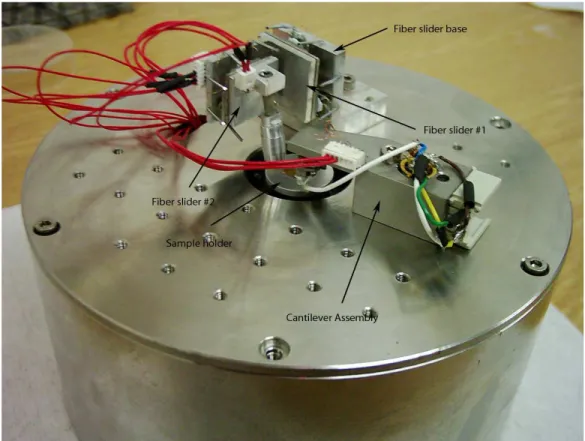
our design, the fiber slider and sample slider designs are fully remade and they are working perfectly. We control all of the translational and rotational motion of the instrument with the computer. The instrument is composed of four main parts:
∗ The sample slider, which is used in both STM and nc-AFM modes ∗ The fiber slider, which is used in nc-AFM mode
∗ The cantilever assembly, which is used in nc-AFM mode ∗ The tunneling tip assembly, which is used in STM mode
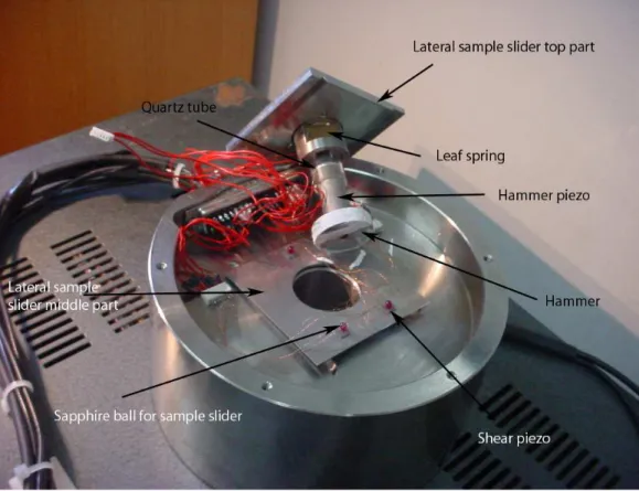
Figure 2.1: A general view of the liquid-air AFM.
2.1.1
The Sample Slider
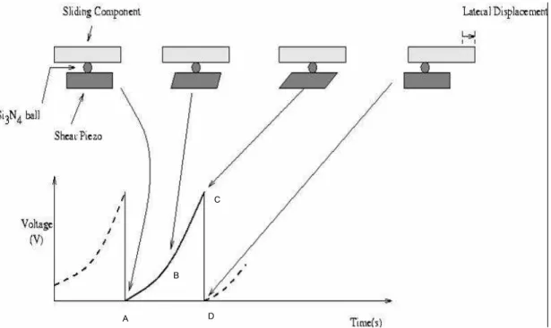
The microscope is a sample-scanning instrument, in which the tip is held station-ary at all times and the sample under the tip is coarse and fine approached to the tip and then scanned for imaging (Figure 2.1). The speed of coarse approach is about 15 µm per second. The lateral coarse motion of the sample is done by piezos that generate shear(shear piezos 5 mm× 5 mm × 1 mm) motion when a voltage is applied between the plates of them [27].
Figure 2.2: The vertical and lateral sample slider.
Three shear piezos are positioned in a triangular pattern, the poles of each of them facing the same direction. Each has a 3 mm diameter synthetic sapphire ball glued on the top surface and the sliding component (sapphire plate) placed on top of the ball (A) to minimize the frictional forces (Figure 2.3). A voltage signal, which gives constant acceleration is applied across the plates of the each piezo, which causes a deformation (B) in the piezo material to a certain direction (in this case to the right) causing a shear movement of the sliding component to the same direction. When the voltage is suddenly reduced to zero (C), the piezos go back to their initial position but the inertia of the sliding component prevents it to go back, it remains stationary, which causes a small lateral displacement (D). The speed of this movement can be controlled by changing the frequency
Figure 2.3: The principle of shear piezoelectric slider
of the voltage signal in the order of 102
Hertz. But higher frequencies cause unpredictable motion and may even damage the instrument. The mechanical resonances of the instrument determines this limit [9]. The polarity of the voltage can be changed to achieve backward movement.
The vertical sample positioning is done by a tube piezo 25 mm long, 12.3 mm in diameter, and 0.5 mm wall thickness. The tube is attached to a quartz tube, which acts as the sliding component, and a metal weight which acts as the hammer. A sawtooth voltage, like the one used to generate lateral motion, is applied to the outer plate of the tube, while the inner surface is grounded. The tube contracts gradually until the maximum voltage is reached (B in Figure 2.3). The glass tube does not slide during this movement. But when the voltage is suddenly reduced to zero, the tube rapidly expands longitudinally moving back to its initial position. During this rapid movement the hammer also moves down,
and this rapid downward movement causes the glass tube to slide upward slightly. As with the lateral movement, the speed of this movement can also be controlled by the frequency and the direction of the movement can be changed by reversing the polarity of the voltage signal.
The fine sample motion is done by a tube scanner 12.7 mm long, 6.35 mm in diameter, and 0.5 mm wall thickness. The outer plate of the tube scanner is divided into four quadrants stretching along the length [28]. The inner plate is intact and covers the whole inner surface. Fine approach is done by applying an increasing voltage to all four outer quadrants simultaneously, which causes the tube to expand and thus approach the tip. A tunneling feedback circuit, which will be explained later, monitors if a specific tunneling current is on. If this condition is met, then the feedback circuit stops the approach.
The sample slider provides coarse and fine movement of the sample. The vertical lateral movement system is attached to the bottom of a spacer which has holes for electrical connections. This spacer is attached to the sliding component, namely the quartz tube, which slides on a circular metal piece, quartz tube holder. The quartz tube is held tight by a leaf spring and touches to the flat portions of the quartz tube holder. The sliding of the quartz tube is done on this three parts of the quartz tube holder. The tube scanner is on top of the spacer. The sample to be scanned is placed on top of the sample holder, which is attached to the top of the tube scanner. The quartz tube holder is attached to the top plate of the lateral sample scanner by three screws, so the movement of the lateral sample slider can be transferred to the quartz tube and then to the sample through tube scanner.
2.1.2
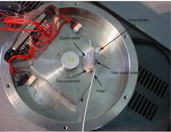
The Fiber Slider
The fiber slider consists of three parts: The first one does the translation and rotation in the y-z plane, the second one does the translation and rotation in the x-z plane and the third part does the fine approach of the fiber to the cantilever. The first two parts takes care of the coarse approach.
The first two parts can be named as the course fiber slider and the designs of them are actually the same, the only difference is that they are placed per-pendicular to each other, which gives us the freedom to move the fiber to almost anywhere within the range of the slider. The range of the course fiber slider is a few mm, which is more than enough.
The principle of movement of the course fiber slider is actually the same as the lateral sample slider(Figure 2.3). We have used 9 shear piezos for each part of the course fiber slider, which are placed on top of each other in groups of three. Their polarities are arranged to provide the desired movements. Conductive adhesive is used between the piezos to provide conductivity. This configuration allows us to move the slider in all four directions and to rotate it in that particular plane. On top of each group of three shear piezos, there is a macor piece with a 1 mm hole in the middle, which is used as the socket of the sliding 1 mm in diameter synthetic sapphire ball. The ball is placed in that hole. The sapphire plate, which is attached to the other part of the course fiber slider slides on top of this sapphire ball. Two Ni plates of 1 mm thickness and a few magnets are used to hold the fiber slider components together.
A tube piezo, dimensions, similar to the hammer piezo, provides the fine motion of the fiber (Figure 2.4). This fine motion is similar to the fine approach of the sample, the only difference is that the fine fiber tube piezo has only two electrodes whereas fine sample tube piezo has five, which are required for scanning the sample. The tube is tilted at an angle of 10◦, the reason of which is going
to be explained later in the cantilever holder part. A hollow metal cylinder is attached to the end of the fiber piezo, which has a few slits along its length to hold the fiber firmly. The fiber is placed in that slit, and the end of it is approached to the reflective surface of the cantilever.
2.1.3
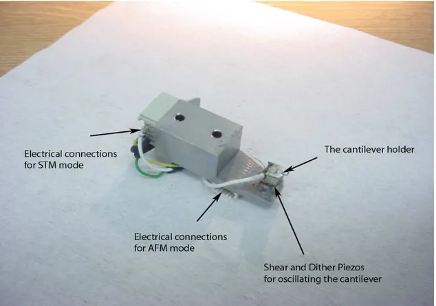
The Cantilever Assembly
The cantilevers are produced by smashing (will be explained in the Cantilever and Tip Preparation section) 50 µm thick tungsten wires, which will provide
Figure 2.4: The x-z fiber slider and fiber piezo.
the reflective surface for optical detection after coating with Au and chemically etching the end of them to be used as the interacting tip of the instrument. Then it is attached to the silicon part, located at the very end of the ceramic substrate, with conductive epoxy to provide the stability and the conductance required for STM feedback. We have used STM feedback, as well as force-distance feedback. An Op-Amp circuit is crucial for the STM feedback to monitor current-voltage characteristics in the tunneling tip-surface vicinity. It operates as an i-V con-vertor. If the sample is electrically conducting then it is possible to use STM feedback. The multi-purpose tip is electrically connected to the Op-Amp which contains a 100 MΩ feedback resistor. This resistor allows the Op-Amp to measure the current with a gain of 108 V
Figure 2.5: The cantilever assembly.
There are two piezo crystals used in the cantilever base assembly (Figure 2.5), one (dither piezo) is used to oscillate the cantilever vertically the other (shear piezo) is used to oscillate it horizontally. They are place on top of each other and conductive adhesive is used to join them to provide the conductivity. The ceramic substrate is tilted by an angle of 10◦ to approach the tip to the
sample surface easily. The fiber piezo is tilted by the same angle to align the end of the fiber and the reflective surface of the cantilever perpendicularly, which is crucial in optical interferometry.
2.1.4
The Tunneling Tip Assembly
This part is used only in STM imaging. The tunneling tip holder is like the STM feedback part of the cantilever assembly, the only difference is that there is no need for a oscillating tip in tunneling tip holder since the only method of imaging is tunneling. So an Op-Amp circuit is also needed in this part to provide the required current-voltage sensitivity. The Op-Amp used in here is the same as the one used in the cantilever assembly.
2.2
Cantilever and Tip Preparation
The tip and cantilever are the most important parts of the instrument because the sensitivity of the experiment is directly related to them. For STM, only tip preparation is sufficient, cantilevers are not required. But for AFM the cantilever is needed as well as the tip.
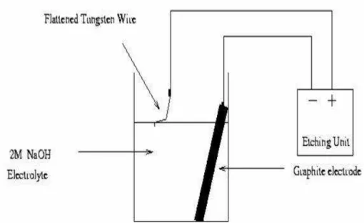
To prepare AFM tip and cantilever, a 50 µm thick tungsten wire is cut into 1 cm pieces. Then, they are placed between two polished metal surfaces, each one encased in carbide to make it possible to compress. After that the metal surfaces are compressed with a vice. This process is called as smashing. This provides the reflective surface of the cantilever. Then the wire is bent 90◦ and put into 2 M
KOH or NaOH solution for electrochemical etching of the tip (Figure 2.6). In this setup, a graphite rod dipped into the solution provides the counter electrode for the tip. Once the circuit is turned on, the etching takes place mostly just under the surface of the solution. So after some time, the part of the wire just under the surface of the solution gets thinner and thinner. The controller circuit cuts the current as soon as the lower part of the wire comes off, creating the sharp tip. Now, the cantilever-tip can be mounted on the ceramic holder. They are attached to the holder using conductive epoxy, which is then exposed to 140 C◦ for ten minutes. This is required to make the joining as stable
Figure 2.6: The electrochemical etching setup.
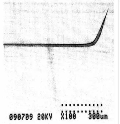
reflective. You can see a photograph of a processed tip in figure 2.7.
2.3
The Interferometer
The design of the interferometer is similar to the interferometer used by Rugar [29, 30]. The specifications of the laser diode is as follows: Its power is 3.8 mW, the wavelength is 1310 nm and the fiber optic cable used is single mode.
The light from the laser diode is split into two with a coupler, the half of the beam goes to a reference photodiode and the other half is sent to the back of the cantilever, and the gold coated back of the cantilever reflects some of this signal back into the fiber optic cable. This signal and the signal reflected from the end of the fiber-optic cable is then sent to a signal photodiode and interfere there. The current generated by the photodiode is given by
Figure 2.7: The electrochemically etched AFM tip.
I = I0(1 − V cos(
4πd
λ )) (2.1)
where λ is the current laser wavelength and d is the separation distance between the end of the fiber and the back of the cantilever. V is fringe visibility and given by V = 2 √ PrPs Pr+ Ps (2.2) and I0 is the average current and given by
Figure 2.8: Schematic diagram of the optical interferometer.
I0 = PavS = (Pr+ Ps)S (2.3)
where Pr is the reference beam power, Ps is the signal power at the photodiode,
P0 is the laser output power and S is the sensitivity of the photodiode. In the
presence of multiple reflections the cosine in the equation 2.1 is replaced by a complex periodic function of d [14].
I = I0(1 − V F (
4πd
The most sensitive operating point is at the quadrature where the fiber-cantilever separation is λ 8, 3λ 8, 5λ
8 .... At this quadrature point, the photocurrent is
affected by the separation distance and wavelength according to
∆I I0 = 4πV ∆d λ − 4πdV ∆λ λ2 (2.5)
The shot noise is given by
dshot = λ 2πV m s eB 2SPav (2.6)
where λ is the wavelength of the laser, e is the electronic charge, B is the detection bandwidth and m is the ratio of the slope of the interference pattern and the slope of regular Michelson fiber optic interferometer system.
2.4
The Control Units
The experiments are controlled and the results are displayed by an electronic control unit and a computer software.
2.4.1
The Electronics Control Unit
The electronics consist of eight PCB cards:
∗ Power supply card supplies various voltages to other cards: 5V , ±8V , ±15V , ±220V and 300V ,
∗ HV card supplies voltages to the sample scanner piezo quadrants,
∗ Slider Card supplies voltages to the sides of the shear piezos used in sample and fiber course slider motion, and also controls fiber fine movement through fiber fine piezo,
∗ Photodetector card with the laser diode, the coupler and the two photode-tectors takes care of the fiber interferometry,
∗ Controller card regulates the tip-surface separation by using STM or AFM feedback,
∗ Digital I/O card communicates with the computer,
∗ Digital to analog converter card(DAC) converts digital signals into analog ones,
∗ Analog to digital converter card(ADC) converts analog signals into digital ones.
2.4.2
The Software: SPM
The software used to perform all of the needed operations is called Scanning Probe Microscopy and written in C + +. It is improved frequently to meet the new requirements of the experimental setup. The program performs fiber and sample coarse approaches as well as the fine approaches, imaging, force-distance spectroscopy. The coarse fiber and sample approaches is controlled by a joystick connected to the electronics. The fine approach of the sample is done automat-ically, which is explained in sample piezo section, and the tip-surface separation is monitored by the feedback circuit.
The interference patterns from the fiber interferometer can be displayed on the screen and saved to the hard disk. The program is capable of keeping the interferometer at the quadrature point, which is very important for sensitivity. This is done as follows: The computer determines a quadrature point from an interference pattern and fiber piezo is used to keep the fiber at the position which provides the laser power at the value specific to that quadrature point.
Before the imaging, the sample is approached to the tip until the preset tun-neling current is found, while a preset bias voltage is applied between the tip and
surface. The feedback loop gain can also be set via the software. By controlling the offset voltages applied to the tube scanner, the position of the tip in the imaging region can be controlled. The data to form the images can be stored in 128 × 128, 256 × 256 or 512 × 512 matrix forms. The separation of the tip and the surface can also be controlled during scanning to keep the tip within the tunneling range. A number of filters such as low pass, median are used to improve the image quality.
Results and Conclusion
We have constructed a new non-contact AFM from scratch, which will be capable of measurements under liquids. We have taken a few preliminary test scans and the results of this scans are going to be shown in this section. All the images are scanned in STM mode, some of the tips are fabricated for AFM measurements. The design of the setup allows STM measurements with AFM cantilevers. A voltage bias between the AFM tip and the surface causes a tunneling current between the AFM tip and the surface, but because the AFM tips must be much more thinner than the STM tip, this type of operation is not advised. The reason behind our attempt to take those images is that we planned to use STM feedback to monitor and keep the tip-surface separation constant, so we have to be sure that imaging with tunneling detection is possible in AFM setup. The samples are all silicon gratings of various dimensions, mostly 4×4µm2
. The images are all taken in ambient conditions, there is not any sound or thermal isolation chamber, so during long scans the gathering dust particles have been a real problem for us. But the experiments are done on a vibration isolation platform, we plan to design or buy a closed chamber for sound and thermal isolation. It is crucial for liquid measurements to keep the humidity of the chamber constant, in order to keep the liquid cell from evaporation.
In the figures 3.1 and 3.2, there is a cut in the middle of the image. This cut means that the tunneling tip is out of range and cannot scan the surface. This
may be caused by a number of reasons: The disturbing ambient conditions such as dust, thermal effects as well as the long vertical range of the sample surface, or the instabilities of tunneling tip.
The white region at the bottom left corner of the figure 3.3 is probably a dust particle, its colour is white since the spacing between the tip and the surface is smaller at the white region, whereas the spacing increases towards darker sides.
The scans in the figures 3.5 and 3.6 are done at the same region with figure 3.3 and figure 3.4, just the scan area is smaller than that of the figure 3.3 and 3.4. The dust particle again shows up in this image.
Figure 3.11 and figure 3.12 are taken by AFM tips, which have to be much more thinner than the STM tip to provide the sensitivity during AFM scans. But thinner tips are also more susceptible to noise beside their high sensitivity. Our scans are all done at ambient conditions, the only isolation is vibrational isolation. Still there is a trace of an orderly pattern in the images. In figure 3.13 and figure 3.14 the pattern is much more clear.
In 3.15 the tip scratches the surface during scanning but somehow manages to detect the hexagonal structure on the surface. It is possible to improve the sensitivity of the tip by touching it to the surface. There is a new science called nanoindentation working on this subject. We do not know what determines a sharp tip after touching to the surface and retracting, which is the one of the main research areas of nanoindentation scientists.
We have demonstrated a number of images taken by our newly constructed STM/AFM. All of the images below have been taken in STM mode some with STM-tip some with AFM-tip. The tunneling current is constant. The images show that the instrument is working, but it still needs to be improved and more experiments are needed to achieve the atomic resolution in air and liquids.
Figure 3.1: STM-tip image of a 4×4 µm2
GaAs grating, Loop Gain: 999, Vertical Range: 2.87 µm, Scan speed: 1 µm/s, Tunneling Current: -0.32 nA, Bias voltage: -0.1 V
Figure 3.3: STM-tip image of a 4×4 µm2
GaAs grating, Loop Gain: 999, Vertical Range: 3.01 µm, Scan speed: 2 µm/s, Tunnelling Current: -0.35 nA, Bias voltage: -0.1 V
Figure 3.5: STM-tip image of a 4×4 µm2
GaAs grating, Loop Gain: 999, Vertical Range: 3 µm, Scan speed: 3 µm/s, Tunneling Current: -0.32 nA, Bias voltage: -0.1 V
Figure 3.7: STM-tip image of a 4×4 µm2
GaAs grating, Loop Gain: 999, Vertical Range: 4.8 µm, Scan speed: 1 µm/s, Tunneling Current: -0.4 nA, Bias voltage: -0.1 V
Figure 3.9: STM-tip image of a 4×4 µm2
GaAs grating, Loop Gain: 999, Vertical Range: 2.72 µm, Scan speed: 1µm/s, Tunneling Current: -0.4 nA, Bias voltage: -0.1 V
Figure 3.11: AFM-tip image of a hexagonal GaAs grating, Loop Gain: 999, Vertical Range: 1.2 µm, Scan speed: 1 µm/s, Tunneling Current: -1.61 nA, Bias voltage: -0.5 V
Figure 3.13: AFM-tip image of a rectangular GaAs grating, Loop Gain: 999, Vertical Range: 2.85 µm, Scan speed: 0.5 µm/s, Tunneling Current: -0.95 nA, Bias voltage: -0.5 V
Figure 3.15: AFM-tip image of a hexagonal silicon grating, Loop Gain: 999, Vertical Range: 1.2 µm, Scan speed: 1 µm/s, Tunneling Current: -1.61 nA, Bias voltage: -0.5 V
[1] K. E. Drexler, Nanosystems (John Wiley and Sons, New York, 1992). [2] G. Binnig and H. Rohrer, Helvetica Physica Acta, 55, 726 (1982).
[3] Roland Wiesendanger, Scanning Probe Microscopy and Spectroscopy (Cam-bridge University Press, Cam(Cam-bridge, 1994).
[4] Stephen Gasiorowicz, Quantum Physics (John Wiley and Sons, Singapore, 1974).
[5] J. Bardeen, Phys. Rev. Lett., 6, 7 (1961).
[6] J. Tersoff and D. R. Hamann, Phys. Rev. B, 31, 805 (1985).
[7] H. Neddermeyer, Scanning Tunnelling Microscopy (Kluwer Academic Pub-lishers, Dordrecht, The Netherlands, 1993).
[8] Dawn A. Bonnell, Scanning Tunnelling Microscopy and Spectroscopy (VCH Publishers, Inc., New York, 1993).
[9] Steve Jeffery, Ph. D Thesis, (Oxford University, Oxford, 2001).
[10] J. H. Coombs and J. B. Pethica, IBM J. Res. Develop., 30, 559 (1986). [11] G. Binnig and C. F. Quate and Ch. Gerber, Phys. Rev. Lett., 56, 930
(1986).
[12] Mehrdad Atabak, M.S. Thesis (Bilkent University, Ankara, 2001). [13] J. Ferrante and J. R. Smith, Phys. Rev. B, 19, 3911 (1979).
[14] ¨Ozg¨ur ¨Ozer, Ph. D. Thesis (Bilkent University, Ankara, 2001). [15] F. F. Abraham, J. Chem. Phys., 68, 3713 (1978).
[16] I. K. Snook and W. van Megen, J. Chem. Phys., 72, 2907 (1980).
[17] J. N. Israelachvili, Intermolecular and Surface Forces (Academic Press, London, 1992).
[18] D. Sarid, Scanning Force Microscopy (Oxford University Press, New York, 1991).
[19] U. Durig, J. K. Gimzewski, D. W. Pohl, Phys. Rev. Lett., 57, 2403 (1986). [20] Y. Martin and C. C. Williams and H. K. Wickramasinghe, Scanning
mi-croscopy, 2, 3 (1988).
[21] R. Erlandson and G. M. McClelland and C. M. Mate and S. Chiang, J. Vac. Sci. Technol. A, 6, 266 (1988).
[22] G. Meyer and N. Amer, Appl. Phys. Lett., 53, 1045 (1988).
[23] C. Julian Chen, Introduction to Scanning Tunnelling Microscopy (Oxford University Press, New York, 1993).
[24] Y. Martin and C. C. Williams and H. K. Wickramasinghe, J. Appl. Phys., 61, 4723 (1987).
[25] T. R. Albrecht and S. Akamine and T.E. Carver and C. F. Quate, J. Vac. Sci. Technol. A, 8, 3386 (1990).
[26] P. M. Hoffman and A. Oral and R. A. Grimble and H. ¨O. ¨Ozer and S. Jeffery and J. B. Pethica, Proc. R. Soc. A, 457, 1161 (2001).
[27] D. W. Pohl, Surf. Sci., 181, 174 (1987).
[28] G. Binnig and D. P. E. Smith, Rev. Sci. Instrum., 57, 1688 (1986).
[29] D. Rugar and H. J. Hamin and R. Erlandsson and J. E. Stern and B. D. Ferris, Rev. Sci. Instrum., 59, 2337 (1988).