PROBE MICROSCOPY
A DISSERTATION SUBMITTED TO THE DEPARTMENT OF PHYSICS AND THE INSTITUTE OF ENGINEERING AND SCIENCE OF BİLKENT UNIVERSITY IN PARTIAL FULFILLMENT OF THE REQUIREMENTS FOR
THE DEGREE OF DOCTOR OF PHILOSOPHY
By Münir Dede September 2008
ii
I certify that I have read this thesis and that in my opinion it is fully adequate, in scope and in quality, as a dissertation for the degree of doctor of philosophy.
Prof. Dr. Ahmet Oral (Supervisor)
I certify that I have read this thesis and that in my opinion it is fully adequate, in scope and in quality, as a dissertation for the degree of doctor of philosophy.
Prof. Dr. Atilla Aydınlı
I certify that I have read this thesis and that in my opinion it is fully adequate, in scope and in quality, as a dissertation for the degree of doctor of philosophy.
iii
I certify that I have read this thesis and that in my opinion it is fully adequate, in scope and in quality, as a dissertation for the degree of doctor of philosophy.
Assoc. Prof. Dr. Oğuz Gülseren
I certify that I have read this thesis and that in my opinion it is fully adequate, in scope and in quality, as a dissertation for the degree of doctor of philosophy.
Assist. Prof. Dr. H. Özgür Özer
Approved for the Institute of Engineering and Sciences:
Prof. Dr. Mehmet Baray
iv
ABSTRACT
DEVELOPMENT OF NANO HALL SENSORS FOR HIGH
RESOLUTION SCANNING HALL PROBE MICROSCOPY
Münir Dede Ph.D in Physics
Supervisor: Prof. Dr. Ahmet Oral September 2008
Scanning Hall Probe Microscopy (SHPM) is a quantitative and non invasive method of local magnetic field measurement for magnetic and superconducting materials with high spatial and field resolution. Since its demonstration in 1992, it is used widely among the scientific community and has already commercialized. In this thesis, fabrication, characterization and SHPM imaging of different nano-Hall sensors produced from heterostructure semiconductors and Bismuth thin films with effective physical probe sizes ranging between 50nm‐1000nm, in a wide temperature range starting from 4.2K up to 425K is presented.
Quartz crystal tuning fork AFM feedback is demonstrated for the first time for SHPM over a large temperature range. Its performance has been analyzed in detail and experiments carried with 1×1μm Hall probes has been successfully shown for a hard disk sample in the temperature range of 4.2K to 425K. Other samples, NdFeB demagnetized magnet, Bi substituted iron garnet and, single crystal BSCCO(2212) High Temperature superconductor were also imaged with this method to show the applicability of the method over a wide range of specimens. By this method, complex production steps proposed in the literature to inspect the non‐conductive samples were avoided.
v
A novel Scanning Hall probe gradiometer has also been developed and a new method to image x, y & z components of the magnetic field on the sample surface has been demonstrated for the first time with 1μm resolution. 3D field distribution of a Hard Disk sample is successfully measured at 77K using this novel approach to prove the concept.
Keywords: Scanning Hall Probe Microscope, Hall Probe, Probe microscopy, SHPM, SOI, GaN, InSb, Quantum well, Bismuth, Quartz tuning fork, STM feedback, AFM feedback, Hall gradiometer, 3D field measurement.
vi
ÖZET
YÜKSEK ÇÖZÜNÜRLÜKLÜ TARAMALI HALL AYGITI
MİKROSKOBU İÇİN NANO HALL ALGILAYICILARIN
GELİŞTİRİLMESİ
Münir Dede Fizik Doktora
Tez Yöneticisi: Prof. Dr. Ahmet Oral Eylül 2008
Taramalı Hall Aygıtı Mikroskobu (THAM), manyetik ve süperiletken malzemeleri yüksek uzaysal ve manyetik alan çözünürlüğü ile inceleyebilen tahribatsız ve nitel bir manyetik görüntüleme yöntemidir. İlk olarak 1992 yılında gösterilen yöntem hızla gelişerek etkin bir manyetik görüntüleme yöntemi olarak kabul görmüş ve ticari ürün haline de getirilmiştir. Bu tezde çeşitli çok katmanlı yarıiletken malzemeler ve Bizmut ince film kullanılarak 50-1000nm aktif fiziksel alana sahip Hall algılayıcıların üretimi, karakterizasyonu ve 4.2-425K sıcaklık aralığında THAM görüntülemesi başarılmıştır.
Elektriksel iletkenliği olmayan örneklerin incelenmesine olanak sağlayan Atomik Kuvvet Mikroskobu (AKM) geri beslemesini kullanmak için Hall aygıtlarının kuvartz kristal çatallara entegrasyonu geniş bir sıcaklık aralığında ilk defa gösterilmiştir. Yöntemin performansı ve çalışma kararlılığı 4.2-425K sıcaklık aralığında fiziksel aktif alan büyüklükleri 1×1μm olan farklı Hall aygıtlarla sabit disk örneği kullanarak başarılı bir biçimde gösterilmiştir. Benzer şekilde Fe katkılı Bizmut, termal olarak de-manyetize edilmiş NdFeB mıknatıs ve BSCCO(2212) tek kristal yüksek sıcaklık süperiletkeni de aynı yöntem ile görüntülenerek yöntemin çok değişik numunelerin incelenmesinde uygulanabilirliği ispatlandı. Geliştirdiğimiz bu yöntem sayesinde literatürde elektriksel
vii
iletkenliği olmayan örnekleri incelemek için önerilen karmaşık mikro-yay üretim yöntemlerine olan gereksinim ortadan kalkmıştır.
Yüzey manyetik alanlarının uzaysal değişimini gözlemlemek için kullanılabilecek özgün bir gradyometre yöntemi ilk defa gösterilmiş ve bu yöntem manyetik alan dağılımının her üç uzaysal bileşenini, x, y ve z, 1μm’lik Hall algılayıcılar yardımı ile görüntülemek için kullanılmıştır. Yöntemin geçerliliğini göstermek için bir sabit disk örneğin manyetik alan profili 77K sıcaklıkta üç boyutlu (3B) olarak haritalandırılmıştır.
Anahtar Sözcükler: Taramalı Hall Aygıtı Mikroskobu, Hall algılayıcı, THAM, Uç mikroskobu, SOI, GaN, Bizmut, InSb, Kuvantum kuyu, Kuvartz kristal çatal, Atomik Kuvvet Mikroskobu (AKM) geri beslemesi, Taramalı Tünelleme Mikroskobu (TTM) geri beslemesi, Hall gradyometre, 3B görüntüleme.
viii
ACKNOWLEDGEMENTS
It is my pleasure to express my sincere gratitude to my supervisor, Prof. Dr. Ahmet Oral for his invaluable guidance, support and opportunities provided beyond the scope of this study.
I also express my deep appreciation to Dr. Rızwan Akram for the scientific discussions and contributions he made to my Ph.D. work.
I would like to thank the members of my thesis committee, Prof. Dr. Atilla Aydınlı, Prof. Dr. Ömer Dağ, Assoc. Prof. Dr. Oğuz Gülseren and Assist. Prof. Dr. H. Özgür Özer for their comments on this thesis.
I am especially thankful to Assoc. Prof. Dr. İsmet İnönü Kaya of Sabancı University for his invaluable help about the e-beam writing system. I also would like to thank to Anıl Günay and Selda Sonuşen of Sabancı University for SEM images.
I would like to thank to Orhan Akar and Prof. Dr. Tayfun Akın of Metu Met for chip dicing.
I like to acknowledge Assoc. Prof .Dr. Marco Affronte and his group members, Alberto Ghirri and Andrea Candini, of University of Modena, Gian Carlo Gazzadi of INFM for the FIB work and the PPMS setup.
I would like to deeply thank to Prof. Dr. Ekmel Özbay and Evren Öztekin of Bilkent Nanotam for their help on wafer dicing.
I also like to acknowledge Prof. Dr. Kazuo Kadowaki of Tsukuba University for BSCCO samples.
ix
I would like to thank to Dr. Ian Farrer and Prof. Dr. David A. Ritchie of Cambridge University for the GaAs HEMT wafers.
I also would like to thank to Prof. Dr. Adarsh Sandhu of Tokyo Institue of Technology, for the InSb wafers and his collaboration on Bismuth FIB milling.
I am thankful to Dr. Jeffrey McCord of IFW Dresden, for the NdFeB sample.
I would like to acknowledge Prof. Dr. Mustafa Ürgen and his group members for their help on FIB milling and hospitality.
I am obliged to thank Assist. Prof. Dr. Hidayet Çetin for his friendship, comments on thin film growth and collaboration on graphene samples.
I am also thankful to Çağrı İşeri for his detailed work on quartz tuning forks and Cosmos simulations.
I am thankful to, The Scientific and Technological Research Council of Turkey (TÜBİTAK), for sponsoring the thesis through the grants 105T473 and 105T501.
I would like to thank our group members Mehrdad Atabak, Özge Girişen, Sevil Özer, Aslı Elidemir and Dr. Özhan Ünverdi, for creating an enjoyable and unique working environment. I would like to acknowledge all the employees of NanoMagnetics Instrument Ltd. for the SHPM setups and for their close collaboration and assistance whenever I needed.
I would also like to thank to Bilkent ARL technicians Murat Güre and Ergün Karaman for their continuous effort in up keeping the clean room setups.
I am indebted to my family for their continuous support, and prayers. And finally, I thank my dearest wife Gülden as she was always beside me. I would like to devote this work to her and my parents.
x
Contents
Chapter 1 : Introduction & Background ... 1
1.1 Introduction ... 1
1.2 Classical Hall Effect ... 3
1.3 Magnetoresistance Effects ... 9
1.4 Bitter Decoration ... 10
1.5 Lorentz Microscopy ... 12
1.6 Magneto-Optical (MO) Imaging ... 14
1.7 Spin Stand Microscopy ... 14
1.8 Scanning Superconducting Quantum Interference Device (SQUID) Microscopy ... 16
1.9 Magnetic Force Microscopy (MFM) ... 17
1.10 Scanning Hall Probe microscopy (SHPM) ... 18
Chapter 2 : The Microscope ... 20
2.1 Introduction ... 20
2.2 The Microscope Body ... 21
2.3 The Hall Probe ... 23
2.4 Approach Mechanism ... 27
2.5 Scanner ... 29
2.6 SHPM Control Electronics & Software ... 32
2.6.1 Head Amplifier ... 33
2.6.2 Power Supply ... 34
xi
2.6.4 High Voltage Amplifier (HV Amps) ... 35
2.6.5 DAC Card ... 36
2.6.6 Slider Card ... 37
2.6.7 MicroController & A/D Card ... 38
2.6.8 Controller Card ... 39
2.6.9 Hall Probe Amplifier Card ... 40
2.6.10 Phase Locked Loop (PLL) Card ... 41
2.6.11 Spare A/D Card ... 43
2.6.12 PCI bus Digital I/O Card ... 43
2.6.13 Software ... 44
Chapter 3 : Fabrication & Characterization ... 45
3.1 Introduction ... 45
3.2 Sample Preparation ... 45
3.3 Active Area Definition ... 47
3.4 Mesa Step Definition ... 53
3.5 Recess Etch ... 54
3.6 Ohmic Contact Metallization ... 55
3.7 STM Tip Metallization ... 58
3.8 Metallization for Bonding ... 60
3.9 Packaging ... 60
3.10 GaN Hall Probes for SHPM ... 61
3.10.1 Introduction ... 61
3.10.2 Fabrication ... 62
xii
3.10.4 Experiments ... 70
3.11 InSb Based Quantum Well Hall Sensors ... 78
3.11.1 Introducion ... 78
3.11.2 Fabrication ... 79
3.11.3 Characterization ... 81
3.11.4 Experiments ... 84
3.12 SOI Hall Sensors for SHPM ... 89
3.12.1 Introduction ... 89
3.12.2 Fabrication ... 90
3.12.3 Characterization ... 92
3.12.4 Experiments ... 99
3.13 Bismuth Thin Film Hall Sensors ... 103
3.13.1 Introduction ... 103
3.13.2 Fabrication & Characterization ... 104
Chapter 4 : Quartz Crystal AFM Feedback for SHPM ... 127
4.1 Introduction ... 127
4.2 Sensor Preparation ... 131
4.3 Characterization ... 133
4.4 Experiments ... 139
Chapter 5 : Hall Probe Gradiometry ... 146
5.1 Introduction ... 146
5.2 Novel Hall Probe Gradiometry ... 150
5.3 Three Dimensional Magnetic Field Imaging ... 159
xiii
List of Figures
Figure 1.1: Schematic layout of the Hall effect on a slab geometry. ... 4 Figure 1.2: Schematic representation of the Hall effect considering the n type carriers. E and EH are the external electric field and Hall field, respectively. ... 8
Figure 1.3: Electron deflection through the sample in Lorentz microscopy ... 13 Figure 1.4: Schematic layout of the Scanning hall Probe Microscope. The common elements of the SPM family can clearly be distinguished. ... 19 Figure 2.1: The design representation of the SHPM with close up details of the scanner head. ... 22 Figure 2.2: Picture of the microscope. The shield, puck & sample holder, slider glass and the piezos are shown. ... 23 Figure 2.3: The alignment of the Hall probe with respect to the sample surface (b). The Hall probe (bottom part) and its reflection of the sample surface first made parallel by alignment screws (a), then the desired angle is given by loosening the screws on the corner of the chip. By this, the same angle is obtained on both sides. Mesa etch can be distinguished on the corner of the chip (a). ... 25 Figure 2.4: Effect of the sample-probe separation on the resolution when the sample is (b) 2.8µm, (c) 1.6µm and (d) 0.4µm. The dependency of the separation (d) with respect to the placement of the Hall cross about the mesa corner (l) is also shown in part (a)... 26 Figure 2.5: Scope trace of high voltage pulse sent to the slider pizeo to slide the puck over the quartz tubing used as a guide. Each square has 50V vertical 2.5ms lateral scale. ... 28 Figure 2.6: Schematic representation of the raster scan over the sample. ... 31 Figure 2.7: The SHPM Control Electronics. ... 32
xiv
Figure 2.8: The Hall voltage amplifier... 33
Figure 2.9: The frequency dependent gain response of OPA111 current to voltage converter. The measurement cycle used while obtaining the graph is shown above... 34
Figure 2.10: Block diagram of Scan DAC card. ... 35
Figure 2.11: Block diagram of HV Amps. ... 36
Figure 2.12: Block diagram of DAC card ... 37
Figure 2.13: Block diagram of slider card ... 38
Figure 2.14: Block diagram of microcontroller A/D card ... 39
Figure 2.15: The block diagram of controller card. ... 40
Figure 2.16: Block diagram of Hall voltage amplifier card. ... 41
Figure 2.17:Block diagram of PLL card ... 42
Figure 2.18: Block diagram of spare A/D card ... 43
Figure 2.19: Screenshot of the SPM control program ... 44
Figure 3.1: Mask designs for Hall cross definition. The whole chip with ohmic pad extensions (a), close up appearance 10µm × 10µm e-beam/FIB template (b), and two different designs of 1µm Hall crosses (c) & (d) are shown. In first generation mask (c), Hall cross and tip separation is 14µm, whereas, in second generation mask (d) this distance is reduced to 8.5µm. The distances are measured from the center of the cross to the mesa corner. Reduction due to side etch is not included. ... 50
Figure 3.2: Examples of Hall cross definitions. A 1µm Hall probe after the develop (a) and when etched (b) is shown. Similarly (c) & (d) show developed and etched probes, respectively, where the probe size is 0.5µm. Given sizes are physical. 1µm probe defined using AZ-MIR701 whereas 0.5µm one is using AZ-1505. In both cases etching is done by CCl2F2 plasma with an etch depth of ~1.2µm ... 51
xv
Figure 3.3: A 10µm × 10µm area isolated by etching for further e-beam process. The four pads have to be separated further until a Hall cross with desired size is obtained. The isolated lead, which appears on the upper left side of the image, is the tip pad. If needed it has to be connected to the corner of the active region where an isolated tip can
be fabricated. ... 52
Figure 3.4. Schematic representation of Hall probe alignment... 53
Figure 3.5: Mesa etch. ... 54
Figure 3.6: Recess etch mask design (a), and etched wafer (b). ... 56
Figure 3.7: Ohmic contacts without (a) and with (b) RTP. The Kirkendall effect after RTP can be seen in part (b). The RTP process was done at 450ºC for 45 sec under forming gas (95%N2, 5%H2) environment. An Ohmic metallization was done to a 2DEG HEMT GaAs sample evaporating 27nm Ge/ 54nm Au/ 6nm Ni /100nm Au. .... 58
Figure 3.8: Tip definition lithography (a) and the tip after lift-off (b) 10nm Cr /50nm Au evaporated for the tip. Connection between the tip lead and the tip is maintained via mesa etch. ... 59
Figure 3.9: Diced & packaged Hall probe. ... 61
Figure 3.10: Schematic diagram of the layer configuration of the AlGaN/GaN heterostructure used ... 64
Figure 3.11: Effect of Hall current on Hall coefficient, RH., as a function of the temperature. ... 66
Figure 3.12: Effect of Temperature on Hall coefficient, RH. as a function of the Hall current, IH. ... 66
Figure 3.13: Hall coefficient for negative drive currents at high temperatures. ... 67
Figure 3.14: Hall coefficient for positive drive currents at high temperatures ... 67
Figure 3.15: Hall voltage (VH) is measured as a function of Hall current (IH), varying the temperature from 22ºC to 150ºC ... 69
xvi
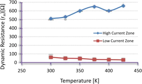
Figure 3.16 Effect of temperature on the dynamic resistances for low current (rHLC)and
high current (rHHC) regions. ... 69
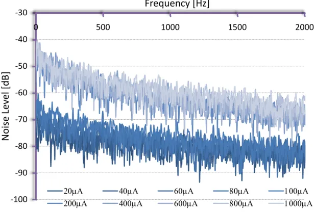
Figure 3.17: Noise power spectrum of GaN probes at 300K for different drive currents. ... 70
Figure 3.18: Hall coefficient stability over time at different ambient temperatures ... 71
Figure 3.19: Hall voltage stability over time at different ambient temperatures. ... 72
Figure 3.20: Serial resistance measured at different ambient temperatures. ... 72
Figure 3.21: SHPM image of hard disk sample at Liquid helium temperature (4.2K) & Liquid Nitrogen Temperature (77K) obtained with GaN Hall probe. ... 73
Figure 3.22: SHPM image of hard disk sample at high temperatures. Scanning speed was 5μm/s. Distortions at 425K are most probably to be due to degradation of epoxy between the HP and tuning fork. ... 75
Figure 3.23: Effect of environment temperature on the resonance frequency and quality factor of the quartz tuning fork. ... 76
Figure 3.24: Stability comparison with respect to the electrical characteristics before and after the scan... 77
Figure 3.25: Stability comparison with respect to the electrical characteristics before and after the scan... 77
Figure 3.26: InSb quantum well wafer structure and band diagram. ... 80
Figure 3.27: Change of Hall coefficient (RH) as a function of different drive currents with respect to the temperature for 1µm × 1µm. sized Hall probe. ... 82
Figure 3.28: Noise spectrum of InSb QW Hall probes at 300K for different bias currents. ... 83
Figure 3.29: Change of Hall coefficient (RH) and the serial resistance (RS) as a function of the temperature for fixed drive current IH=100 µA ... 84
xvii
Figure 3.30: Resonance frequency curve of the 32.768kHz quartz crystal tuning fork loaded with 1.25 mm. × 1.25 mm. × 0.5 mm. InSb QW Hall sensor. ... 85 Figure 3.31: HDD SHPM scan image obtained at room temperature. The magnetic field profile (a) and the surface topography (b) obtained simultaneously. The scan parameters are; area: 55µm × 55µm, speed: 5µm/sec., resolution: 256×256 pixels, mode: AFM tracking ... 86 Figure 3.32: NdFeB permanent magnet image scanned at room temperature. The scan parameters are; area: 55µm × 55µm, speed: 5µm/sec., resolution: 256×256 pixels, mode: lift off ... 87 Figure 3.33: High temperature scan of Hard disk sample (a) 25ºC (b) 125ºC ... 88 Figure 3.34: Effect of material thickness on Hall coefficient with respect to the carrier density, calculated based on the parameters of the used SOI wafer. ... 92 Figure 3.35: Effect of device thickness on the magnetic flux noise spectrum vs. frequency at 25oC with fixed bias current of 500μA. ... 93 Figure 3.36: Effect of bias current on the magnetic flux noise spectrum vs. frequency at 25oC. ... 94 Figure 3.37: Effect of the temperature on the magnetic flux density noise spectrum vs. frequency with fixed bias current of 500μA. ... 95 Figure 3.38: Effect of Temperature on the VH vs. IH characteristics. rHHC and rHLC is the
dynamic resistance defined as the slope of curve in high current (IH> 100μA) and low
current (IH<100μA) regime. ... 96
Figure 3.39: Effect of device thicknesses on the VH vs. IH characteristics. ... 96
Figure 3.40: Change of series resistance Rs with respect to temperature for a Hall device
thickness of 405nm. ... 97 Figure 3.40: Effect of Temperature on the Hall coefficient vs. Hall current. ... 98
xviii
Figure 3.42: Effect of device layer thickness on the Hall coefficient vs. Hall current characteristics. ... 98 Figure 3.43: SHPM image of hard disk sample using (a) QTF AFM and (b) STM feedback at 25oC, with scanning speed of 5μm/s. Device thickness was 405nm. ... 100 Figure 3.44: SHPM image of hard disk drive sample at high temperatures (50-100°C) using QTF AFM feedback. ... 102 Figure 3.45: Change in resonance frequency and the quality of the quartz crystal tuning fork loaded by a 1 mm × 1mm × 0.5 mm Si Hall probe. ... 102 Figure 3.46: Ohmic contact metallization with (a) and without (b) mesa step. ... 107 Figure 3.47: Image reversal lithography for active area definition (a) and the thin film obtained by thermal evaporation followed by lift off (b)... 108 Figure 3.48: STM tip metallization. ... 109 Figure 3.49: SEM images of FIB patterned typical 50nm × 50nm Bi Hall probe. The STM tip Hall cross center distance is ~4µm. ... 110 Figure 3.50: RT-SHPM image of Bi substituted iron garnet sample obtained by 50nm sized Bi Hall probe. Image size is 8×8µm and the vertical scale from bright to dark is ±55G... 111 Figure 3.51: Mounting Hall sensors on a 1” sized sample holder. PCBs were mounted by double sided carbon tape. Grounding between the top layer of the PCBs and the holder was obtained by aluminum tape pieces and carbon paste. ... 112 Figure 3.52: Effect of charging. The line definitions were not sharp as the beam profile could not be adjusted sharp enough and had a wide Gaussian shape. ... 113 Figure 3.53: Accumulation of Gallium on the surface due to overexposure. Bubble formation around the exposed areas is the sign of accumulation. ... 113
xix
Figure 3.54: Images of a typical FIB patterned Hall probe at ×1000 (a), ×5000 (b), ×20000 (c), and ×50000 (d) magnifications. Overall chip, mesa, Ohmic pads and the STM tip can be seen. ... 114 Figure 3.55: Image of FIB patterned Hall probe at ×20000 (a), with close up display of Hall cross (b) ... 115 Figure 3.56: Temperature depended change in Hall coefficient of ~100nm sized Bi Hall probes. ... 116 Figure 3.57: Noise spectral density pattern of the probes measured through the scope ... 117 Figure 3.58: Noise spectrum of the ~80nm thick ~100nm sized Bi hall probe at 200K as a function of the frequency. ... 118 Figure 3.59: Noise spectrum of the ~80nm thick ~100nm sized Bi hall probe at 100K as a function of the frequency. ... 119 Figure 3.60: Minimum detectable magnetic field of ~100nm sized Bi probe as a function of the applied bias current at 200K ... 120 Figure 3.61: Minimum detectable magnetic field of ~100nm sized Bi probe as a function of the applied bias current at 100K ... 120 Figure 3.62: Solid drawing of the e-beam pattern designed for 100nm wide Hall probes. The shape composed of 23 individual rectangles. Different index colors gives ability to expose at different dose values in a single drawing. ... 122 Figure 3.63: 100nm Hall probe fabricated by e-beam lithography and Bizmuth thermal evaporation & lift-off. ... 126 Figure 4.1: Top (a) ands side (b) view of the quartz tuning fork Hall probe combined sensor after packaging. ... 132 Figure 4.2: One prong free (a) and two prongs free (b) configurations of combined sensors. ... 134
xx
Figure 4.3: First 5 vibration modes of two prongs free configuration obtained by finite element analysis. ... 135 Figure 4.4: First 5 vibration modes of one prong free configuration obtained by finite element analysis. ... 136 Figure 4.5: Frequency response of 32kHz Quartz Tuning fork with integrated Hall probe under fix prong and free prong configuration. The effect of scan piezo is also shown. ... 137 Figure 4.6: Side view (a) and corner view (b) of the sample-probe alignment ... 140 Figure 4.7: Autotune curves of the tuning forks. ... 140 Figure 4.8: SHPM image of (a) iron garnet crystal and (b) NdFeB demagnetised magnet obtained in AFM Tracking mode at 300K. Size of the images and vertical scale of the images are (a) 40×40µm & 62 Gauss and (b) 52×30µm & 12,868 Gauss, respectively ... 142 Figure 4.9: SHPM image of (a) Hard disk specimen and (b) simultaneously obtained topography at 300K. Size of the images are 50×50µm and vertical scales are (a) 209 Gauss and (b) 127nm. Vertical scale for the topography shows the relative values. ... 143 Figure 4.10: SHPM image of Hard disk specimen gathered by AFM tracking at 4.2K. Sizes of the images are 16 µm × 16µm and vertical scales are 312 Gauss and 170nm for magnetic (a) and topographic (b) images respectively. ... 144 Figure 4.11: SHPM image of single crystal BSCCO 2212 specimen at 4.2K obtained in lift-off mode. Scan area is 16×16µm and vertical scale is 1.65 Gauss. Image shown is the average of 25 images. ... 145 Figure 5.1: A Hall plate in the integrated circuit technology. A magnetic field perpendicular to the chip surface generates a Hall voltage between the two voltage electrodes of the Hall sensor [95]. ... 147 Figure 5.2: Cut through of a 1D integrated vertical Hall device. This sensor is sensitive to a magnetic field parallel to the chip surface [95]. ... 148
xxi
Figure 5.3: Two vertical Hall sensors placed in a cross shape (2D), used to measure a magnetic field in X and Y directions. ... 148 Figure 5.4: Hall gradiometer. ... 151 Figure 5.5: Hall effect with non-perpendicular current and voltage leads with different configurations under uniform magnetic field... 152 Figure 5.6: Hall effect with non-perpendicular current and voltage leads with different configurations under non-uniform magnetic field. ... 153 Figure 5.7: Orientation of the Hall sensor, over the sample, with respect to the scan direction of the microscope: Hall cross has 45° alignment. ... 155 Figure 5.8: SHPM scan of a Hard disk sample at 77K with normal Hall sensor configuration of mutually perpendicular current and voltage leads. Hall cross diagram shows the relative alignment of the probe over the sample and the leads’ positions. .. 155 Figure 5.9: Calculated ∂Bz/∂x from the measured Bz(x,y) data matrix by forward
differences. ... 157 Figure 5.10: Calculated ∂Bz/∂y from the measured Bz(x,y) data matrix by forward
differences. ... 157 Figure 5.11: SHPM scan of a HDD at 77K with Hall sensor configuration shown in the diagram. The image represents ∂Bz/∂x due to the relative positions of current and
voltage leads ... 158 Figure 5.12: SHPM scan of a HDD at 77K with Hall sensor configuration shown in the diagram. The image represents ∂Bz/∂y due to the relative positions of current and
voltage leads. ... 158 Figure 5.13: Visualization of incremental scan for Bz(x,y,z), ∂Bz(x,y,z)/∂x and
∂Bz(x,y,z)/∂y ... 161
Figure 5.14: SHPM image of Hard disk sample, (a) forward scan (in the tunneling range) and (b) backward scan (3.5µm away from the surface). Both images were
xxii
obtained with STM feedback. Scan speed was 5µm/s, resolution set to 256 × 256 pixels, -100mV bias voltage applied to the sample and the tunneling current of 1nA maintained during the scan. ... 163 Figure 5.15: SHPM images of Hard disk sample obtained at room temperature showing effect of the thermal drift. Pictures are the forward scans of probe above the sample with a height of (a) 0.5µm, (b) 1.5µm, (c) 2.5µm, (d) 3.5µm respectively. Field decay is not seen as the offset is only given during the backward scan. Approximately 4 hours of time passed between the shown images. The shift is towards the bottom left corner. All images were obtained with STM feedback using a 1µm PHEMT sensor. Scan speed was 5µm/s, resolution set to 256 × 256 pixels, -100mV bias voltage applied to the sample and the tunneling current of 1nA maintained during the scan. ... 164 Figure 5.16: SHPM images of Hard disk sample obtained at 77K showing effect of the thermal drift. Pictures are the scans of probe levels above the sample with a height of (a) 0.25 µm, (b) 1.25µm, (c) 2.5µm, (d) 3.75µm respectively. Approximately 10 hours passed between the first and the last images. There is a very little drift which becomes insignificant after thermal stabilization. All images were obtained using a 1µm PHEMT sensor. Scan speed was 5µm/s, resolution set to 256 × 256 pixels. The decay of the magnetic field can also be seen as the sensors moves away from the sample. ... 165 Figure 5.17: SHPM image of Hard disk sample, shows the Bz of the field (a), obtained
at 77K in the feedback tracking zone. Image was obtained using a 1µm PHEMT sensor. Scan speed was 5µm/s, resolution set to 256×256 pixels. ∂Bz(x,y)/∂x (b) and
∂Bz(x,y)/∂y (c) are calculated from Bz image by differentiating rows and columns of the
image matrix respectively. ... 166 Figure 5.18: By field calculated by integrating ∂Bz/∂y over a finite range. Each image
file used in calculation was obtained using the same 1µm PHEMT sensor. Scan speed was 5µm/s, resolution set to 256×256 pixels. The increments along the z-direction, h, is set to 0.25μm in the range of [0, 6.5μm]. ... 167
xxiii
Figure 5.19: Bx field calculated by integrating ∂Bz/∂x over a finite range. Each image
file used in calculation was obtained using the same 1µm PHEMT sensor. Scan speed was 5µm/s, resolution set to 256×256 pixels. The increments along the z-direction, h, is set to 0.25μm in the range of [0, 6.5μm]. ... 168
xxiv
List of Tables
Table 1.1: Worldwide production of original information, if stored digitally, in terabytes circa 2002. Upper estimates assume information is digitally scanned, lower estimates assume digital content has been compressed [20]. ... 15 Table 3.1: Process parameters of the photoresists used in active area definition ... 49 Table 3.2: Typical Channel Electron Properties at 295K [54] ... 79 Table 3.3: RIE etch parameters for InSb... 81 Table 4.1: Summary of the used parameters and calculation / simulations results for QTFs. ... 138
Chapter 1 : Introduction & Background
The purpose of this chapter is to give an overview about a number of existing and commonly used techniques for magnetic characterization and magnetic imaging, along with the underlying physical interactions in a non comprehensive way. The methods mentioned are not necessarily a probing technique. For the methods used in domain observation “Magnetic Domains: The analysis of Magnetic Microstructure” by Hubert & Schafer has an excellent and detailed discussion addressing the relevant literature [1]. A review paper by Simon J. Bending [2] describes the local probing methods used for vortex imaging in superconductors. The “Magnetic Imaging” Chapter edited by Wolfgang Kuch of the book “Magnetism: A Synchrotron Radiation Approach” [3] and the relevant chapter of the book “Methods in materials research : a current protocols publication” [4] can be also consulted for more detailed information.
1.1 Introduction
The history of the Scanning Probe Microscopes (SPMs) started with the invention of Scanning Tunneling Microscope (STM) in 1981 by Binnig and Rohrer [5]. In this technique an atomically sharp conductive tip is brought in to close proximity of a conductive sample. Classically electrons are not expected to overcome the potential barrier. But, we know, from the quantum mechanics, that there exist a non zero possibility for electrons to tunnel the air or vacuum gap between the tip and the sample. The tunneling current is exponential function of the height of the tip over the sample. Thus, if the current is fed in to a control circuit it is possible to control the height of the tip. By this way a sample surface could be scanned with atomic resolution. This invention not only made it possible to resolve the atoms at the surfaces, but also brought new possibilities to the investigation of the surfaces using different probe-sample interactions. Shortly after the invention of STM, a new method, the Atomic Force
Microscope (AFM) , utilizing force interactions between tip and sample, has been invented [6]. In AFM the conductive tip is replaced by a non- conductive tip attached to the end of a cantilever. The AFM is sensitive to the forces between the tip and the sample, which deflects the cantilever and is measured through an optical system . After AFM many different methods developed to examine different properties through various tip-surface interactions.
Probing techniques have also found applications in magnetism studies. Although it is possible to get information about the magnetic properties of the materials with macroscopic measurements, it is only possible to interpret them further with the aid of local measurement techniques done at the microscopic level. Especially, the measurements performed on magnetic domains on the local scale helps to link the basic physical properties of the matter to its macroscopic properties and the practical applications. The analysis of magnetization curve of a material, for example, requires a basic understanding of the domain structure, that is microscopic regions of identical magnetization direction, of that material [1]. Magnetic imaging techniques allow the most direct visualization of magnetic properties on a microscopic scale and material properties can be studied.
Different classifications can be done for the magnetic imaging techniques considering the way in which depth sensitivity is achieved; the way in which the lateral information is acquired and the physical interaction with the sample magnetization [3]. The first two classification schemes are not interesting in the context of this thesis. The depth sensitivity is a measure of how deep the surface penetrated, and the information extracted from that depth, by the technique used. In other words it represents the probing depth. The way in which the lateral information is acquired, on the other hand, is relevant whether the sample surface is scanned or directly imaged. Classification with respect to the physical interaction includes the physical phenomenon which lies behind the measurement.
The scanning quantum interference device, SQUID, microscope for example, measures magnetic flux, the Hall probe measures magnetic stray field, and the magnetic force microscope (MFM) measures the gradient of the magnetic field convolved with the magnetic moment of the cantilever tip. Since, the force on the electrons due to the stray fled of the sample is the physical interaction in Scanning Hall Probe Microscopy (SHPM), first a simple background information about the underlying physics is needed.
1.2 Classical Hall Effect
The Hall effect is a charge transport phenomenon discovered by an American physicist Edwin Herbert Hall in 1879 [7] during his PhD thesis work and named after him. Before we examine the underlying physics behind the effect, a historical background can help to understand the scientific environment in which the discovery is done. First of all, despite to the fact that it was proposed by Greek scientists two millennia ago and George Johnstone Stoney [8] in 1874 as the minimum quantity of the electricity, the electrons were not known to exist at the time of the discovery. They are later discovered by Joseph John Thomson in 1897 at Cavendish Laboratory [9]. Electron charge is first quantified by Robert Andrews Millikan in 1909 with his famous oil drop experiment [10] and the results are further improved later in 1913 [11]. (For the full history of discovery of electron, the paper by Robotti [12] gives an excellent review). The force on the current carrying conductors, under the magnetic field was formulated by Andre Marie Ampere, Felix Savart, and Jean Baptiste Biot, well before the discovery of the Hall effect.
Edwin Hall found a contradictory sentence while reading James Clerk Maxwell’s classical book Electricity and Magnetism [13]. There was a sentence stating that the magnetic force on the current carrying conductors does not act on the electric current but, on the conductor which carries the current. However, this was against to the very practical observation that conductors generally are not affected by a magnet while not
bearing a current. Also, the strength of the effect is directly proportional to the amount of the current passed. Hence, for a double conclusion, Hall proposed an experiment suggesting “If the current of the electricity in a fixed conductor is itself attracted by a magnet, the current should be drawn to one side of the wire, and therefore the resistance experienced should be increased”. Motivated with this; Hall, conducted series of experiments finally concluding that current tends to move towards the side of the conductor.
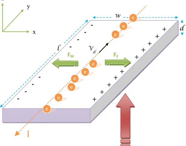
In order to examine the physics of the classical Hall effect, charge carrier slab, as shown in Fig. 1.1, with the dimensions l×w×d can be considered. When a current passes through a conductor in the –y direction, placed in a uniform external magnetic field perpendicular to the direction of the current, charges are deflected due to the Lorentz Force under the presence of this magnetic field.
Figure 1.1: Schematic layout of the Hall effect on a slab geometry.
d
l
w
+
+
+
+
+
+
+
+
+
+
-
-
-
-
-
-
-
-
F
EF
Mz
y
x
VdI
e e e e e e e e eElectrons flow is in opposite direction to the current flow, in +y direction. Thus, as the current flows from high to low potential, electrons will flow from low to high electric potential. While flowing through the conductor, the presence of the external magnetic field deflects the electrons towards the left side of the slab with the Lorentz force
(1.1)
Accumulation of electrons on the left hand side of the slab creates a charge imbalance, which in turn makes that side negatively charged. This will in turn generate an electric field until the electric force due to the field balances the magnetic force. The total force on the electron can be written as the total Lorenz Force,
(1.2)
which should become zero. For the sake of simplicity we can assume all the carriers to be the electrons with a charge –e and they all move with the same average drift velocity, d. Thermal effects can also be excluded for the time being. The electrons are also
treated as point particles. Equipped with these, the drift velocity can be visualized as the speed of electrons passing through the section of the conductor with a cross-sectional area A, (w×d) and length l in a time t. So,
(1.3)
Total charge, Q, in that slab is,
(1.4)
where N is the number of electrons per unit volume in the slab. The current, by definition, is the flow of total charge per unit time,
(1.5)
then,
(1.6)
Thus, current flowing through the slab can be written as,
(1.7)
(1.8)
(1.9)
where j is the current density. However, in general the drift velocity also depends on the other parameters. To have the charges flow, there must be a potential difference across the charge holding material. This potential difference creates an electric field E defined by,
(1.10)
And the drift velocity can be defined as average velocity gained by the current carrying particles due to the presence of the electric field. The proportionality constant of the linear relation between the drift velocity and the electric field known as the mobility, . Mobility is defined by the scattering mechanisms (defects, impurities, phonons etc.) of the material and has unique characteristics. Electron mobility, or the mobility itself in general, is the proportionality constant between the charge density and conductivity.
(1.11)
(1.12)
Mobility is strong function of the defects and the temperature (lattice vibrations). Matthiessen’s rule formulizes that relation as
(1.13)
This is an empirical rule, stating that the resistivity is sum of the resistivity due to the impurities and the resistivity due the lattice.
Going back to the Hall effect, we see that the Lorentz force creates an accumulation of electrons on one side of the conductor. As the charge neutrality condition should be satisfied, accumulated electrons will induce positive charges at the other side of the slab and these will create a potential difference across the width of the sample and thus an electric field which is called as Hall field, EH (Fig. 1.2). Presence of this field forces the
excess charges to decrease at that side of the slab and eventually a balance between transverse electric and magnetic forces nulls the net force. Hence,
(1.14)
0 (1.15)
Figure 1.2: Schematic representation of the Hall effect considering the n type carriers. E and EHare the external electric field and Hall field, respectively.
̂ (1.17) (1.18) (1.19) (1.20) (1.21)
E
E
Hv
d-V
HI
Hz
y
x
+
+
+
+
+
+
+
--
-
-
-
-RH, the proportionality factor of the equation, is called as the Hall coefficient. It
depends on the free carrier concentration in the material. Measurement of coefficient by applying a know magnetic field, B perpendicular to the slab and measuring the Hall voltage VH and its polarity , enable us to obtain free charge density and its type ( n or
p-type) of the material. The sign of the Hall coefficient represents the majority of the charge carriers.
1.3 Magnetoresistance Effects
Magnetoresistors are a class of the materials which undergo a resistance change with the applied magnetic field. If the variation of the resistance can be calibrated with respect to the applied field strength they can be used as a magnetic field gauge or sensor. This dependence is generally non-linear [14]. Fabrication of small probes allows this method to be useful at local magnetization measurements. All the current Hard Disks use Giant Magnetoresistance (GMR) sensors for read heads and the discovery of this effect by Albert Fert and Peter Grünberg were awarded with the Nobel Prize in Physics in 2007. Tunneling magnetoresistance (TMR) Sensors are estimated to replace the GMR sensors, as they show much higher change in resistance, as high as 450%, compared to the GMR sensors.
GMR is based on the weak coupling between thin ferromagnetic films separated by a normal non-magnetic metal in which the resistance of certain materials drops dramatically as a magnetic field is applied. The effect is usually seen in magnetic multilayered structures, where two or more magnetic layers are closely separated by a thin spacer layer a few nm thick. An electron with certain spin state is allowed to pass through the first magnetic layer. If the second magnetic layer is aligned in a similar way then that electrons can easily pass through the structure, and the resistance is low. If the second magnetic layer is misaligned then neither spin channel can get through the structure easily so the electrical resistance is high. This can be repeated by successive
stacking of more than two layers. So, when an external field is applied to ferromagnetic stacks oriented anti-parallel, that shows a high resistance in the absence of the field, becomes parallel exhibiting the same direction of magnetization with a low resistance. Electrons spin in one of two directions, up or down, which corresponds to the North and South poles of a magnetic field.
Anisotropic magnetoresistance (AMR) on the other hand, depends on the angle between magnetisation and current density in a thin permalloy film. The physical origin of AMR effect is the different shift of the energy levels of electrons with a positive and negative spins, respectively, under the influence of a magnetic field. This leads to a shift in the Fermi levels [15].
Extraordinary magnetoresistance (EMR) is produced by sandwiching a thin layer of highly conducting metal like gold between layers of nonmagnetic semiconducting materials. The EMR effect is due to the magnetic field induced current redistribution between the semiconductor and the metal [16]. The change of the resistance was as high as 100 – 75,0000 % in fields ranging from 0.05 to 4T for symmetric van der Pauw disk at room temperature [17].
Ballistic magnetoresistance is produced at the junction of two nanowires. Because the junction is only a few hundred atoms wide, electrons flow straight through rather than bouncing from side to side the way electrons flow through larger wires. The change in resistance is greater than 3,000 percent, and the small size of the sensor makes it possible to read tiny, closely-packed bits [18]
1.4 Bitter Decoration
Bitter or powder pattern imaging of domain structures is the oldest imaging technique proposed by Bitter in 1931 [19]. Bitter used Fe2O3 particles of ~1µm in size suspended
in ethyl acetate to observe the stray fields on different ferromagnetic substances. The technique is based on covering the surface with a colloidal suspension of magnetic particles. The particles collect and agglomerate in regions where large stray fields from the sample are present, typically over domain walls. Then the pattern can be imaged using an optical microscope or an electron microscope depending on the size of the patterns. Success of the method mainly depends of the preparation of the magnetic colloids. A good colloid can have particles of ~10nm enriched by various surfactants to aid better surface adhesion [1]. Another method to cover the surface with fine particles consist of evaporation of ferromagnetic particles from a filament [2]. A filament made of ferromagnetic materials, usually iron, nickel or cobalt, placed a few centimeters away from the sample used to form a magnetic vapor in a low pressure helium environment. The particles in the vapor travel to the sample surface and arrange themselves according to the present inhomogeneous field distribution. Since the spatial resolution is limited by the particle size in colloid, we can say that the resolution can be ~10nm theoretically. Usually 100nm spatial resolution is practically achievable. Note that, although the bittern decoration gives a direct visualization of the size and shape of the domain patterns, no information can be extracted about the magnitude and the direction of magnetization. Another difficulty should be highlighted is related to the sample preparation. The technique cannot distinguish between the real topography and the stray field distribution of the sample. Thus, fine polishing or chemical treatment of the specimen is necessary. The ferrofluid or evaporated ferromagnetic particles can stick to the surface and may prevent further use of that sample or it might be required to re-clean the sample before it is used for another experiment. In that sense bitter decoration is an invasive imaging method. The Bitter decoration is limited to low field values, typically less than 10mT [2] and only works if the sample has stray field [1].
1.5 Lorentz Microscopy
Lorentz microscopy is a special type of the imaging that uses transmission electron microscopy (TEM). While use of conventional SEM requires no special sample preparation, for TEM the samples must be thinned to ~70nm (depends on the acceleration voltage used) and the samples must be conductive up to some degree as required in most of electron based techniques. In electron microscopy the electrons emitted from the filament are accelerated to high energies of 100-200keV in the standard TEMs. These energies can go up to 1MeV in some high voltage transmission electron microscopes [1]. Electrons also has the wave nature and their wavelength can be as small as 0.0123 Å, which is much smaller than inter atomic spacing [1]. Thus, while analyzing, it is possible to use the particle or wave aspect of the electrons. If we consider the particle aspect than classically the electron will interact with magnetic field according to well known Lorentz force and they will be deflected. In that case only the perpendicular component of the magnetic field to the direction of motion of electrons is effective on the deflection. The Lorentz microscopy is based on these deflections along the path of the electrons due to magnetic fields in the specimen. However the interpretation of this deflection may be different depending on the used method. First method is defocused or Fresnel mode Lorentz imaging. The name is given because the magnetic contrast obtained is based on the Fresnel effect. While electrons are passing through the sample they are deflected in directions depending on the magnetization direction of each domain. Thus, the distribution of the domains throughout the sample consequently deflects and superposes the electrons in constructive or destructive manner creating bright or dark parts due to the wave nature of the electrons. This effect can be observed while the microscope is defocused since, only defocused images contain angular information. Note that the method only works if the domain walls are parallel to the magnetization axis. When they are perpendicular no net deflection can be achieved. In other method used, instead of defocusing the image diffraction pattern is formed at one of the aperture planes of the microscope which is called in focus or Foucault
method. A selective imaging can be obtained by changing the position of the aperture. This will allow electrons deflected only with certain angle to form the bright or dark field. Hence, prediction about the magnetization direction is possible
Figure 1.3: Electron deflection through the sample in Lorentz microscopy
Differential phase microscopy, on the other hand, is a special case of the Lorentz technique which can achieve ~2 nm resolution [4]. To use this technique a TEM should be modified to measure the Lorentz deflection with quadrant electron detector. The deflection is measured through the differences of the currents created on the quadrants of the detector, which gives the name to the method.
Common to all the Lorentz Microscopy methods described above, we can say that they all give high resolution images are sensitive to small variations of the magnetization. However, the limitations or the negative aspects have to be considered as well. First of all the method require a huge amount of investment on the microscopes. Sample preparation is difficult and may require special tools as well which in turn increases the budget further. The magnetic fields used to deflect or condense the electron beams
Incident Electrons
should have a special arrangement not to interfere with the surface magnetization of the samples so that the electron beams are not affected by these fields.
1.6 Magneto-Optical (MO) Imaging
Magneto-optical imaging is a general term used for broad family of magnetic imaging methods that are based on the small rotations of the polarization plane of the polarized light and only visible when viewed with a polarization microscope. The interaction of polarized light with the magnetization structure of the material causes the plane of polarization to rotate. If the rotation of the polarization plane happens due to reflection of light then this is the Kerr effect. On the contrary, if the rotation of the linearly polarized light is in transmission, than the effect is called Faraday effect. The sensitivity of this method is mainly limited by the optical parts of the used microscope. Other limitation comes from the MO material and how good they are brought into contact with the sample. If a laser is used instead of the conventional optical system, this can increase the resolution and can give better flexibility in terms of the post processing. But they are slower compared to the classical systems and heating of the sample due to higher power can be a problem [1]. But modern pulsed lasers have made it possible to capture images at rates of 10 ns frame [4]. Typical resolution is around 0.3μm [1, 4] in a high quality optical microscope using an oil immersion objective and blue light illumination [4]. Sample preparation is also important. To enhance the resolution samples must be optically flat and damage free. Nevertheless, MO is more or less a non-invasive technique which gives direct and fast observation of the magnetization.
1.7 Spin Stand Microscopy
A study carried out by the faculty and students at the School of Information Management and Systems at the University of California at Berkeley shows that about 5 exabytes (1 exabyte = 1018 bytes) of new information was created in 2002 and 92% of
this information is stored in magnetic media [20]. To rationalize the number it worth to note that Library of Congress contain about 136 terabytes of information; five exabytes of information is equivalent in size to the information contained in 37,000 new libraries the size of the Library of Congress book collections! Table 1.1 summarizes yearly worldwide production of original stored content.
Table 1.1: Worldwide production of original information, if stored digitally, in terabytes circa 2002. Upper estimates assume information is digitally scanned, lower estimates assume digital content has been compressed [20].
Storage Medium 2002 Terabytes Upper Estimate 2002 Terabytes Lower Estimate 1999‐2000 Upper Estimate 1999‐2000 Lower Estimate % Change Upper Estimates Paper 1,634 327 1,200 240 36% Film 420,254 76,69 431,690 58,209 ‐3% Magnetic 5187130 3,416,230 2,779,760 2,073,760 87% Optical 103 51 81 29 28% TOTAL: 5,609,121 3,416,281 3,212,731 2,132,238 74.5%
From this table, we can conclude that currently, hard disk drives are the dominant magnetic storage devices because they offer the best overall combination in non-volatility, reliability, large capacity, high data transfer rate, and low production cost. The development in hard disk drive (HDD) industry brings the technological advancement of hard disk drives. A hard disk is composed of many parts having different functions which require a joint study of different branches of science and engineering to continue advancement. This multi-disciplinary scheme contains studies from physics, material science, aeronautical engineering, computer sciences etc. One of the important aspects about developing the HDDs is the control of data writing on the ferromagnetic material used for data storage in hard disk. Inspection done on this subject can help to improve the new materials to be employed as a storage medium, to
characterize write/read heads. In that sense, the spin stand microscopy is one of the methods specifically developed to serve the HDD research and industry. The imaging is done with a sensor brought in to very close proximity of the HDD while the disk is mounted on a spin stand. Visualization of the bits is done with high speed at a few hundred nanometer scale resolution. In fact it is very similar to the real working principle of an HDD. The sensor used in spin-stand microscopy technique is a conventional magnetoresistive read/write head. Images are acquired by scanning a certain portion of the rotating disk in the along-track and cross-track directions [21]. If the along-track direction is scanned, while the disk is rotated, cross-track direction scanning is performed by using radial displacements of the head with the voice coil.
1.8 Scanning Superconducting Quantum Interference
Device (SQUID) Microscopy
The superconducting quantum interference device, SQUID, is by far the most sensitive sensor of magnetic flux reaching a resolution of 10-21 Wb(Tesla m2). Magnetic field resolution of SQUIDs can be as low as fT/√Hz with a pickup coil are of a few square millimeter [22].
There are two main types of SQUIDs, which are DC and RF SQUIDs. The distinction comes from the number of Josephson junctions used. RF SQUIDs can work with only one Josephson junction, whereas DC SQUIDs need two junctions. Josephson junctions are the weak links separating a superconducting loop which form the detection part of the device.
When it is brought close to the sample, external flux generated by the specimen penetrates the SQUID loop. To maintain the flux quantization condition the SQUID loop should generate a current which circulates through the loop. This circulating current will cause one of the Josephson junctions to exceed its critical current, and a
voltage will develop across the SQUID. This voltage triggers the feedback systems and a current Ifeedback is supplied by the feedback circuit with a known mutual inductance L.
The feedback flux Φfeedback= L× Ifeedback required to keep voltage generated through the
loop minimized is equal to the applied flux through the SQUID that generated the signal [23]. The SQUID should be positioned as close as possible to the sample to achieve a high spatial resolution [24, 25]. It is also important to have a small effective area of the loop. A recently reported nano-SQUID has a spatial resolution of substantially less than 0.5µ m with field resolution of ~10 nT [26].
1.9 Magnetic Force Microscopy (MFM)
Magnetic force microscopy is a modified atomic force microscope sensitive to the magnetostatic forces instead of atomic forces (AFM). A first demonstration of MFM goes back to 1987 [27, 28]. In this method forces are measured by a deflection of magnetically coated cantilever very similar to the conventional AFM [6]. Deflection of the cantilever can be measured in several ways including the use of piezoresistive cantilevers or by optically deflecting a laser beam from the back of the cantilever. The difference to AFM comes with the tip which is coated with a ferromagnetic material. The coating must be optimized in accordance with the inspected sample. The sample and tip brought together with the aid of the usual AFM approach techniques. When the surface is reached, the designated area can be scanned with the help of the piezo scanners. Usually a lift off technique developed by Digital Instruments is employed. In this scan method first the surface topography is scanned by AFM feedback along the forward scan. Then up on completion of the topographic profiling a certain height is given to lift the scanner and the surface is scanned again following its texture with the given offset in the backward scan direction. By this way the effect of the short range forces are eliminated and the van der Walls forces are kept at constant level. Interaction between the tip and the sample is not very straightforward. It includes magnetization distribution of the tip that interacts with the stray field of the sample. However, it can be
hard to quantify the components of the interactions as the tip itself may be dominating over the samples stray field due to its high magnetization. So it is not straightforward to obtain quantitative images. Nevertheless, although the information about the magnetization distribution in a sample is only indirect, MFM is probably the most widely used magnetic imaging method. Main reason for this is ease use of the microscope under various environmental conditions, its high spatial resolution, which also gives topographic information, and the commercial availability of instruments.
1.10 Scanning Hall Probe microscopy (SHPM)
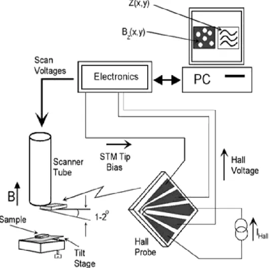
The first realization of this method is given by Chang et al. in 1992 [29]. Since then the methods is spreading among the science community and already commercialized [30].
In SHPM as shown in Figure 1.4, a Hall probe integrated with an STM tip is brought in to close proximity of the sample under inspection using the course approach mechanism. The sample is tilted ~1-2º about the probe to have the STM tip at the highest position. Integrated STM tip keeps track of the surface just like in the case of STM seeking a tunneling current. The tunneling current is fed into a control electronic to maintain a constant current changing the height of the sensor with respect to the topography of the sample using a piezo tube scanner. The simultaneous topography and magnetic imaging can be accomplished while scanning the designated area within the scan range of the piezo. Overall control of approach and scan is maintained via dedicated SHPM control electronic and software. It is also possible to use AFM feedback as explained in Chapter 4, which makes it possible to scan non-conductive samples for simultaneous topography and magnetic data. Integration of Hall probes with quartz tuning fork force sensors are demonstrated here.
The technique can give quantitative data with a high spatial resolution [31]. Microscope can work in a wide temperature range under high magnetic fields [32]. The detailed
description of the method and sensor fabrication is given in Chapter 2 and Chapter 3 respectively. Achievement of 50nm spatial resolution using Bismuth thin film and FIB milling is described in Chapter 3 together with the fabrication of other semiconducting materials selected as candidates for SHPM imaging. Chapter 5, on the other hand shows the first demonstration of the novel Hall gradiometer and its use to obtain all the spatial components of the magnetic field over a hard disk sample with 700nm spatial resolution.
Figure 1.4: Schematic layout of the Scanning hall Probe Microscope. The common elements of the SPM family can clearly be distinguished.
Chapter 2 : The Microscope
This chapter explains the details of the Scanning Hall Probe Microscope (SHPM) used in this thesis. The microscope body, electronic control unit and the acquisition & control software are introduced. The details of the electronics are kept brief aiming to guide the reader in a general sense of functionality. The details of the sensor, coarse approach and scan mechanisms are also given.
2.1 Introduction
Scanning Hall Probe Microscope SHPM is a member of the Scanning Probe Microscopy (SPM) family and shares the common characteristics of these instruments. Although different subfield classifications are possible with respect to the interaction used or property measured, SPM in general, refers to techniques that use the interaction of a probe (or sensor) with the surface of a sample to measure various characteristics; surface conductivity, static charge distribution, localized friction, magnetic fields, elastic moduli etc, of the sample at nanometer scale, in some cases atomic resolution. Thus, whatever the technique is used or property is inspected, there are a set of common elements used in all the SPMs. These common properties can be listed as,
1. The Probe (sensor),
2. Coarse approach Mechanism, 3. Scanner Mechanism,
4. Control Electronics & Software.
The following sections briefly explain these particular elements in general sense with details specific to the microscope employed in this thesis. The microscope used is
commercially available [30] Scanning Hall Probe Microscope (SHPM), developed in collaboration with our group.
2.2 The Microscope Body
The microscope body is an assembly housing all the mechanical parts, moving or stationary, which forms the microscope. Scanner and coarse approach mechanisms, electrical connectors and cabling are all brought together to form the microscope. The microscope has been shaped according to the application requirements. The microscope used in this study has a compact form in order to fit in to cryostat systems for low temperature applications. Radiation baffles decrease the effect of the radiation from 300K reaching the head and help preserve the cryogen. The extension tube is designed to bring the scan head to the magnet center of the cryostat. It also houses all the cables used to carry the signal in and out to the SHPM head. Approach and scanner elements are located on the head as shown in Fig. 2.1 & 2.2. The sample is placed on the sample holder facing towards the sensor, which is mechanically attached to the slider puck. The puck is, then, engaged over the slider glass tube by properly tightened the leaf spring. The puck, which is held by static friction, is free to move along the slider tube. The hollow cylindrical shield is placed around the whole head to mechanically protect the scanner, to help maintaining the temperature stability and it shields the system from the electromagnetic noise.
Leaf Spring Quartz Slider Slider Piezo Scanner Piezo Sample Holder Radıatıon BAffels Extension Flange
Figure 2.1: The design representation of the SHPM with close up details of the scanner head.
Figure 2.2: Picture of the microscope. The shield, puck & sample holder, slider glass and the piezos are shown.
2.3 The Hall Probe
The first, and may be the most important, element is the sensor. The probe is specially fabricated to be sensitive to a specific property aimed for measurement and interfaces the sample with the rest of the microscope. The probe, in this application, is a Hall sensor, which is sensitive to the perpendicular component of the stray magnetic field on the surface of the magnetic or superconducting samples. The working principle and the production details of Hall sensors are given in related sections of the thesis. Use of other type of sensors is also possible depending on the property need to be measured provided that the right electrical connections are done. We can use the microscope as STM, AFM and MFM, replacing the Hall probe with appropriate sensor. The fabricated Hall sensors
are mounted on a non magnetic printed circuit board (PCB) that has suitable electrical connections to the rest of the microscope cabling with spring probes mating at the back of the PCB. The PCB sensor holder and the sensor isolated electrically by placing a piece of alumina ceramic sheet in between. Electrical connections from the probe to PCB are achieved by 12μm gold wires using ultrasonic wedge bonder. The sensor holder is, then screwed at the end of a piezoelectric scanner to map the field over the sample. To pick a proper magnetic signal the probe should be as parallel as possible to the sample. On the other hand the mesa corner, which is used as a crude STM or AFM tip, must be in closest position to the sample. To satisfy both requirements, the sample is tilted 1-1.5° with respect to the probe. There are set of three screws on the sample puck to achieve this. Increasing the tilt angle more than ~3° may cause the chip edges to touch the sample. Also, increasing the angle increase the separation of the active region and decrease the magnetic signal. On the other hand if the angle is set lower than 1°, defects or spikes left from the fabrication can touch the surface and create unwanted signals by shorting the current or voltage leads of the Hall sensor to the sample bias voltage or can increase the probe–sample separation.
Probe-sample separation is important in terms of both spatial resolution and field sensitivity. Spatial sensitivity is the ability to resolve the fine magnetic structures on the sample. In that sense, the smaller the Hall probe size, the better resolution is obtained. Nevertheless, if the probe sample separation is bigger than the size of the cross, that is the size of active Hall area, aimed structural resolution cannot be obtained. In addition to that, the field decays with the distance and quantification of it is not possible when the probe is far from the sample. This distinction can clearly be seen in the images given in Fig. 2.4, where a thermally demagnetized NdFeB permanent magnet is imaged at various probe sample separations. The probe separation is higher when the Hall cross is away from the tip corner. Thus to increase the resolution the Hall cross must be brought as close as possible to the mesa corner of the chip. Field resolution, on the other hand, does not depend on the probe sample separation. Existence of an external magnetic field creates
(a)
(b)
Figure 2.3: The alignment of the Hall probe with respect to the sample surface (b). The Hall probe (bottom part) and its reflection of the sample surface first made parallel by alignment screws (a), then the desired angle is given by loosening the screws on the corner of the chip. By this, the same angle is obtained on both sides. Mesa etch can be distinguished on the corner of the chip (a).
(a)
(b) (c) (d)
Figure 2.4: Effect of the sample-probe separation on the resolution when the sample is (b) 2.8µm, (c) 1.6µm and (d) 0.4µm. The dependency of the separation (d) with respect to the placement of the Hall cross about the mesa corner (l) is also shown in part (a).
the Hall voltage signal. The main noise component of this signal comes from the Johnson noise which is generated by the thermal agitation of the charge carriers [33]. Johnson noise is defined by

![Figure 3.14: Hall coefficient for positive drive currents at high temperatures 0510152025300320340360380 400Hall Coefficient (Rh) [mΩ/G]Temperature [K]](https://thumb-eu.123doks.com/thumbv2/9libnet/5671237.113561/91.892.187.791.648.1010/figure-hall-coefficient-positive-currents-temperatures-coefficient-temperature.webp)