2015 IEEE 35th International Conference on Electronics and Nanotechnology (ELNANO)
218
Hollow-Cathode Plasma-Assisted Atomic Layer
Deposition: a Novel Route for Low-Temperature
Synthesis of Crystalline III-Nitride Thin
Films and Nanostructures
Necmi Biyikli, Cagla Ozgit-Akgun, Eda Goldenberg,
Ali Haider, Seda Kizir, Tamer Uyar
National Nanotechnology Research Center (UNAM) Institute of Materials Science and Nanotechnology
Bilkent University, Bilkent, Ankara, Turkey [email protected]
Sami Bolat, Burak Tekcan, Ali Kemal Okyay
Department of Electrical and Electronics Engineering &National Nanotechnology Research Center (UNAM) Institute of Materials Science and Nanotechnology
Bilkent University, Bilkent, Ankara, Turkey [email protected]
Abstract — Hollow cathode plasma-assisted atomic layer
deposition is a promising technique for obtaining III-nitride thin films with low impurity concentrations at low temperatures. Here we report our efforts on the development of HCPA-ALD processes for III-nitrides together with the properties of resulting thin films and nanostructures. The content will further include nylon 6,6/GaN core/shell and BN/AlN bishell hollow nanofibers, proof-of-concept thin film transistors and UV photodetectors fabricated using HCPA-ALD-grown GaN layers, as well as early results for InN thin films deposited by HCPA-ALD technique.
Keywords — III-nitride, atomic layer deposition, hollow cathode plasma, nanofibers, thin film transistors, photodetectors
I. INTRODUCTION
Plasma-assisted atomic layer deposition (PA-ALD) is a cyclic, low-temperature thin film deposition method, in which the substrate surface is exposed to sequential pulses of precursor molecules and plasma species separated by evacuation and/or purging periods. When compared to other techniques, PA-ALD stands out with its self-limiting growth mechanism, which enables the deposition of highly uniform and conformal thin films with sub-angstrom thickness control. Layer-by-layer growth offered by PA-ALD further enables the deposition of alloy thin films with well-defined compositions. These features make PA-ALD a promising technique not only for the low-temperature deposition of III-nitrides and their alloys on temperature-sensitive device layers/substrates and post-CMOS processing, but on nanostructured templates as well for the synthesis of III-nitride nanostructures [1-3].
Recently, our group reported the PA-ALD of polycrystalline wurtzite AlN thin films at temperatures ranging from 100-500°C using a quartz-based inductively coupled RF-plasma (ICP) source [4-6]. AlN thin films deposited using trimethylaluminum (AlMe3) as the Al precursor at temperatures within the ALD window (100-200°C for both NH3 and N2/H2 processes) were C-free and had relatively low O concentrations (<3 %) as determined by X-ray photoelectron spectroscopy
(XPS).We also demonstrated the conformality of AlMe3-NH3 plasma process by fabricating high surface area AlN hollow nanofibers using electrospun nylon 6,6 nanofibrous mats as sacrificial templates, which might potentially be used in high temperature ambient chemical sensing applications [7]. Our initial efforts for depositing GaN thin films, however, resulted in amorphous thin films with high O concentrations (~20 %) [8,9]. The source of this O contamination was found to be related to the sputtering of quartz tube of the ICP source. In view of these circumstances, the choice of N-containing plasma gas (N2, N2/H2 or NH3) determined the severity of O incorporation into the deposited thin films [10]. In order to avoid this contamination problem, we integrated a stainless steel hollow cathode plasma (HCP) source to the ALD system, and thereby reported the hollow cathode PA-ALD (HCPA-ALD) of nanocrystalline AIN and GaN thin films with low impurity concentrations at 200 °C using trimethylmetal precursors [11]. Within the scope of the same study, AlxGal-xN thin films were also deposited via digital alloying, which alloy composition was determined by the relative number of AlN and GaN subcycles in the main HCPA-ALD cycle.
In this paper, we review our efforts on the development of HCPA-ALD processes for III-nitrides together with the properties of resulting thin films and nanostructures. The content will further include nylon 6,6/GaN core/shell and BN/AlN bishell hollow nanofibers, proof-of-concept thin film transistors (TFTs) and UV photodetectors fabricated using HCPA-ALD-grown GaN layers, as well as InN thin films deposited by HCPA-ALD technique.
II. MATERIALS AND METHODS
AlN, GaN, AlxGa1-xN, and InN thin films were deposited at 200°C in a Fiji F200-LL ALD reactor (Ultratech/ CambridgeNanoTech Inc.) equipped with a stainless steel hollow cathode plasma (HCP) source (Meaglow Ltd.) on Si substrates. Metalorganic precursors, namely trimethylaluminum (AlMe3), trimethylgallium (GaMe3), trimethylindium (InMe3,
2015 IEEE 35th International Conference on Electronics and Nanotechnology (ELNANO)
219 Sigma Aldrich, SAFC Hitech), and cyclopentadienyl indium (CpIn, Strem Chemicals) were used as the group-III source materials. AlMe3 and InMe3 were used at room temperature; whereas GaMe3 was cooled down to 6 °C using a home-made Peltier cooling system, and CpIn was heated to 85 °C. 5N-grade NH3, N2 and H2 plasma gases, and the carrier gas, Ar, were further purified using MicroTorr gas purifiers. Metalorganic precursor pulses and plasma gases were carried from separate lines by 30 and 100 sccm Ar, respectively. The base pressure was ~150 mTorr. Prior to depositions, substrates were cleaned by sequential ultrasonic agitation in 2-propanol, acetone, methanol, and deionized (DI) water. For the native oxide removal, Si (100) and Si (111) substrates were further dipped into dilute hydrofluoric acid solution (HF, 2 vol. %) for ~2 min, then rinsed with DI water and dried with N2. The details regarding to the preparation of electrospun nylon 6,6 nanofiber templates are given elsewhere [10].
Ellipsometric spectra of AlN, GaN, AlxGa1-xN, and InN thin films were recorded at three angles of incidence (65°, 70°, and 75°) using a variable angle spectroscopic ellipsometer (V-VASE, J.A. Woollam Co.). Optical constants and film thicknesses of AlN, GaN and AlxGa1-xN were extracted using the Cauchy dispersion function, whereas B-Spline model was used for the InN thin films. Chemical compositions and bonding states were determined by XPS using a Thermo Scientific K-Alpha spectrometer with a monochromatized Al Kα X-ray source. The pass energy, step size and spot size were 30 eV, 0.1 eV and 400 mm, respectively. Etching of the samples was carried out in situ with a beam of Ar ions having an acceleration voltage of 1 kV. X-ray reflectivity (XRR) and grazing-incidence X-ray diffraction (GIXRD) measurements were carried out with a PANalytical X'Pert PRO MRD diffractometer using Cu Kα radiation. XRR data were fitted by the PANalytical X'Pert Reflectivity Software. A FEI Tecnai G2 F30 transmission electron microscope (TEM) was used at an operating voltage of 300 kV for the imaging and selected area electron diffraction (SAED) analyses of samples. Thin film samples were prepared using an FEI Nova 600i Nanolab focused ionbeam (FIB) system at an acceleration voltage of 30 kV, using various beam currents ranging from 50 pA to 21 nA. Core/shell nylon 6,6/GaN nanofibrous mats, on the other hand, were first put into a solvent (i.e., ethanol) and sonicated. Nanofiber-containing solvent was then drop casted onto a copper grid and allowed to dry. An atomic force microscope (AFM, Park Systems XE-100) operating in the contact mode and Quanta 200 FEG scanning electron microscope (SEM) were used to reveal surface morphologies of the deposited thin films. Samples were coated with ~5 nm Au/Pd alloy prior to SEM imaging.
III. RESULTS AND DISCUSSION
In a recent study, we demonstrated the HCPA-ALD of crystalline AlN, GaN and AlxGa1-xN thin films at low temperature (200 °C) using trimethylmetal precursors and NH3 or N2/H2 plasma [14]. Depositions carried out using non-optimized parameters resulted in AlN and GaN films with wafer-level non-uniformities <±1.5 %. XPS survey scans detected 2.5-3.0 and 1.5-1.7 % O in the bulk of AlN and GaN films, respectively. C was detected only at the film surfaces and there were no C impurities in the bulk films as determined
by XPS. Complementary secondary ion mass spectroscopy (SIMS) analyses performed on the films deposited using NH3 plasma revealed the presence of O, C (both <1 %) and H impurities in the films. GIXRD patterns exhibited polycrystalline AlN and GaN thin films with wurtzite crystal structure. Crystallite sizes were 19.2 and 24.8 nm for AlN, and 10.2 and 9.3 nm for GaN films deposited using NH3 and N2/H2 plasma, respectively. HCPA-ALD parameters were optimized at 200°C; trimethylmetal precursor and N2/H2 saturation curves evidenced the self-limiting growth of AlN and GaN at this temperature. AlN exhibited linear growth with a slight nucleation delay. The growth per cycle (GPC) of AlN was high (~1.0 Å). In the case of GaN, the GPC decreased with the increasing number of deposition cycles, which indicates substrate-enhanced growth. The GPC was found to be 0.22 Å for the 900-cycle GaN deposition. 59.2 nm thick AlN and 20.1 nm thick GaN thin films deposited using optimized process parameters were characterized using spectroscopic ellipsometry, high-resolution XPS, GIXRD, XRR, and AFM. Refractive indices of AlN and GaN thin films were determined to be 1.94 and 2.17 at 632 nm, respectively. Al 2p (Ga 3d) and N 1s high-resolution XPS spectra confirmed the metal nitride bonding states in AlN (GaN) films. The mass densities of AlN and GaN thin films were estimated to be 2.82 and 5.86 g/cm3 using XRR. Rms roughness values determined by XRR were higher than those directly measured using AFM; i.e. 1.97 and 0.64 nm for AlN and GaN thin films deposited on Si (100) substrates, respectively. Within the context of the same study, AlxGa1-xN thin films were also obtained via digital alloying, where the main HCPA-ALD cycle consisted of different numbers of AlN and GaN subcycles. Alloy compositions were determined by Vegard's rule as 0.68 (AlN:GaN = 1:3), 0.95 (1:1), and 0.96 (3:1) using the c lattice parameters, which were roughly calculated from the (002) peak positions. Refractive index values of the AlxGa1-xN thin films decreased from 2.03 to 1.96 as the Al content increased from 0.68 to 0.96. The adjustability of band edge values with alloy composition has been confirmed by optical transmission measurements, which indicated absorption-free films whose optical band edge values shift to lower wavelengths with increasing Al content.
In order to demonstrate the feasibility of HCPA-ALD method for the preparation of three-dimensional (3D) III-nitride nanostructures, we deposited GaN on organic nanofibers prepared by electrospinning. 1000 cycles were deposited on electrospun nylon 6,6 nanofibers having ~70 nm average fiber diameter at 200 °C using GaMe3 and N2/H2 plasma as the Ga and N precursors, respectively. TEM image of the resulting nylon 6,6/GaN core/shell nanofibers is given in Fig. 1. As seen from this figure, conformal GaN coatings with uniform wall thickness along the fiber axis were obtained. High-resolution TEM images and SAED pattern confirmed the polycrystalline structure of deposited GaN layer.
Recently, we have reported GaN-based transistors with the lowest thermal budget reported so far. In this study, we used HCPA-ALD-grown GaN layers in TFTs having bottom gate configuration [16]. Gate stack was formed on a highly doped Si (1-5 mΩ-cm) substrate at a single ALD step performed at 200 °C including the deposition of Al2O3 (77 nm) and GaN (11 nm) as the insulator and semiconductor, respectively.
2015 IEEE 35th International Conference on Electronics and Nanotechnology (ELNANO)
220 Output characteristics of the proposed device revealed the clear saturation and pinch off of the drain current with the increased drain voltage. Transfer characteristics showed that the fabricated device has an ION/IOFF of 2×10³. Threshold voltage, subthreshold swing and channel mobility of the device were found to be 11.8 V, 3.3 V/dec and 0.025 cm2/V·sec, respectively. The effect of the positive gate bias stress on the threshold voltage was also investigated and threshold voltage shift lower than 8 V after a bias of 250 MV/cm for 1000s was obtained.
Fig. 1. Representative TEM image of nylon 6,6/GaN core/shell nanofibers.
In another study, we fabricated proof-of-concept metal-semiconductor-metal (MSM) UV photodetectors using HCPA-ALD-grown GaN layers [15]. Contacts were formed on top of as-grown films with Ti/Au (20 nm/100 nm) electrodes using sputtering after photolithography. Electrical current-voltage measurements showed low dark current voltages as low as 3 pA at 30V reverse bias. Optical characteristics of the devices were also studied. Devices showed 15x rejection ratio comparing UV/VIS wavelengths. Responsivity spectrum was in agreement with optical absorption spectrum of HCPA-ALD-grown GaN films. These devices can pave the way for temperature sensitive processes such as flexible optoelectronics as well as CMOS integration of such devices.
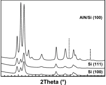
800 cycles InN were deposited on Si (100), Si (111) and HCPA-ALD-grown AlN/Si (100) substrates at 200 °C using 1 s CpIn/10 s Ar purge/40 s, 50+50 sccm, 300 W N2/H2plasma/10 s Ar purge. The deposition was done twice, as the 4th and 59th runs following the integration of HPC source. Film deposited on Si (100) substrate as a result of the 4th run was found to be composed of tetragonal In (t-In) and cubic In2O3 (c-In2O3) phases; whereas for the sample deposited on AlN/Si (100) substrate, GIXRD results indicated the existence of wurtzite (hexagonal) InN (h-InN) phase in addition to the t-In and c-In2O3. Films deposited as a result of the 59th run, on the other hand, were identified as polycrystalline, single-phase h-InN
irrespective of the substrate (Fig. 2). The formation oft-In and c-In2O3 phases is believed to be due to the residual water in the deposition chamber, which was scavenged by the metalorganic pulses during the runs between the two identical depositions. XRR results obtained from h-InN thin film deposited on Si (111) substrate indicated negligible thickness and a quite low mass density for this film. Surface morphology studies performed using AFM also evidenced the formation of InN islands on Si (111). For the film deposited on AlN/Si (100) substrate, thicknesses of the InN and In2O3 layers were estimated as 34.87 and 0.08 nm, respectively. Mass density of the deposited InN was found to be 2.89 g/cm3, which is very low compared to the recognized value of 6.81 g/cm3 [14]. XRR measurements revealed the surface roughness as 3 nm, which is in good agreement with the AFM measurements that indicated a continuous film with 3.14 nm rms surface roughness as measured from a 1 μm × 1 μm scan area.
Fig. 2. GIXRD patterns of InN thin films deposited at 200 °C on various substrates using CpIn and N2/H2 plasma.
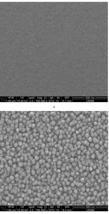
Another set of InN thin films were deposited on Si (100) substrates at 200 °C using InMe3 as the indium precursor. 1000 cycles were deposited, where one HCPA-ALD cycle was 0.03 s InMe3/10 s Ar purge/40 s, 50+50 sccm (or 50 sccm), 300 W N2/H2 (or N2) plasma/10 s Ar purge. GIXRD results indicated polycrystalline thin films; the film deposited using.
N2/H2 plasma was found to be composed of h-InN and t-In phases, whereas the film deposited using N2 plasma was identified as single-phase h-InN. Polycrystalline structure of this h-InN film was further confirmed by high-resolution TEM and SAED. Thickness, mass density and surface roughness values of the films deposited using N2/H2 and N2 plasma were estimated using XRR as 59.3 and 42.7 nm, 4.52 and 6.56 g/cm3, and 5.58 and 2.06 nm, respectively. Thickness values were further confirmed by spectroscopic ellipsometry measurements. The surface roughness values obtained using XRR were in good agreement with the corresponding surface morphologies (Fig. 3).
XPS survey scans obtained after 60 s of Ar ion etching indicated that there were no C impurities in the films. For the
2015 IEEE 35th International Conference on Electronics and Nanotechnology (ELNANO)
221 film deposited using N2 plasma, there were no O impurities either; however ~21 % O was detected in the film deposited using N2/H2 plasma. This high oxygen concentration might be associatedwith the 3D surface oxide layer.
a
b
Fig. 3. Plan-view SEM images of InN films deposited at 200 °C on Si (100) substrates using (a) InMe3-N2 plasma and (b) InMe3-N2/H2 plasma processes.
CONCLUSION
Here we reviewed our previous and current efforts on the development of PA-ALD processes for III-nitride thin films and their alloys using a HCP source for creating reactive N species. We successfully deposited polycrystalline wurtzite AlN, GaN and AlxGa1-xN thin films with low impurity concentrations at temperatures as low as 200 °C using metalorganic group-III precursors. The feasibility of HCPA-ALD technique for the preparation of 3D III-nitride nanostructures was demonstrated via nylon 6,6/GaN core/shell nanofibers. Proof-of-concept TFTs and MSM UV photodetectors, which were fabricated using HCPA-ALD-grown GaN layers, were also presented. Preliminary experiments have shown that InMe3-N2 plasma HCPA-ALD process on a Si (100) substrate results in polycrystalline wurtzite InN thin film with low impurity concentrations and a smooth surface morphology with low roughness value.
ACKNOWLEDGMENTS
This work was performed at UNAM – Institute of Materials Science and Nanotechnology. A.K.O. and N.B. acknowledge the financial support from TUBITAK (Project #112M004 and 112M482). F.K. thanks to TUBITAK-BIDEB 2211 for a PhD scholarship. M. Guler from UNAM is acknowledged for TEM sample preparation and HR-TEM imaging.
REFERENCES [1] R.L. Puurunen, J. Appl. Phys., 2005, 97, 121301.
[2] S. Y. Yang, G. Jeon, and J. K. Kim, J. Mater. Chem., 2012, 22, 23017. [3] L. K. Tan, X. Liu, and H. Gao, J. Mater. Chem., 2011, 21, 11084. [4] C. Ozgit, I. Donmez, M. Alevli, and N. Biyikli, Thin Solid Films 520,
2750 (2012).
[5] M. Alevli, C. Ozgit, I. Donmez, and N. Biyikli, Phys. Status Solidi A 209, 266 (2012).
[6] M. Alevli, C. Ozgit, I. Donmez, and N. Biyikli, J. Cryst. Growth 335, 51 (2011).
[7] C. Ozgit-Akgun, F. Kayaci, I. Donmez, T. Uyar, and N. Biyikli, J. Am. Ceram.Soc.96, 916 (2013).
[8] C. Ozgit, I. Donmez, M. Alevli, and N. Biyikli, J. Vac. Sci. Technol. A 30, 01A124 (2012).
[9] C. Ozgit, I. Donmez, and N. Biyikli, Acta Phys. Pol.A 120, A55 (2011). [10] C. Ozgit-Akgun, I. Donmez, and N. Biyikli, ECS Trans. 58, 289 (2013). [11] C. Ozgit-Akgun, E. Goldenberg, A. K. Okyay, and N. Biyikli, J. Mater.
Chem. C 2, 2123 (2014).
[12] E. Goldenberg, C. Ozgit-Akgun, N. Biyikli, and A. K. Okyay, J. Vac. Sci. Technol. A 32, 031508 (2014).
[13] S. Bolat, C. Ozgit-Akgun, B. Tekcan, N. Biyikli, and A. K. Okyay, Appl. Phys. Lett. 104, 243505 (2014).
[14] M. E. Levinshtein, S. L. Rumyantsev, and M. S. Shur, Properties of Advanced Semiconductor Materials (Wiley, New York, 2001), p. 4 [15] Burak Tekcan, Cagla Ozgit-Akgun, Sami Bolat, Necmi Biyikli, Ali K.