Appl. Phys. Lett. 93, 123506 (2008); https://doi.org/10.1063/1.2988824 93, 123506
© 2008 American Institute of Physics.
A 500 MHz carbon nanotube transistor
oscillator
Cite as: Appl. Phys. Lett. 93, 123506 (2008); https://doi.org/10.1063/1.2988824
Submitted: 23 June 2008 . Accepted: 04 September 2008 . Published Online: 23 September 2008 A. A. Pesetski, J. E. Baumgardner, S. V. Krishnaswamy, H. Zhang, J. D. Adam, C. Kocabas, T. Banks, and J. A. Rogers
ARTICLES YOU MAY BE INTERESTED IN
Mixing at using a single-walled carbon nanotube transistor
Applied Physics Letters 87, 153111 (2005); https://doi.org/10.1063/1.2103391
80 GHz field-effect transistors produced using high purity semiconducting single-walled carbon nanotubes
Applied Physics Letters 94, 243505 (2009); https://doi.org/10.1063/1.3155212
Analytical ballistic theory of carbon nanotube transistors: Experimental validation, device physics, parameter extraction, and performance projection
A 500 MHz carbon nanotube transistor oscillator
A. A. Pesetski,1J. E. Baumgardner,1S. V. Krishnaswamy,1H. Zhang,1J. D. Adam,1,a兲 C. Kocabas,2T. Banks,2and J. A. Rogers2
1
Northrop Grumman Electronics Systems, 1212 Winterson Road, Linthicum, Maryland 21090, USA 2
University of Illinois, Urbana-Champaign, Illinois 61801, USA
共Received 23 June 2008; accepted 4 September 2008; published online 23 September 2008兲 Operation of a carbon nanotube field effect transistor共FET兲 oscillator at a record frequency of 500 MHz is described. The FET was fabricated using a large parallel array of single-walled nanotubes grown by chemical vapor deposition on ST-quartz substrates. Matching of the gate capacitance with a series inductor enabled greater than unity net oscillator loop gain to be achieved at 500 MHz. © 2008 American Institute of Physics.关DOI:10.1063/1.2988824兴
Carbon nanotube 共CNT兲 field effect transistors 共FETs兲 promise operation at microwave frequencies and beyond with highly linear gain and low power dissipation.1However, because of their high impedance, FETs comprising single nanotubes cannot be measured directly at microwave fre-quencies with conventional 50 ⍀ test equipment such as a network analyzer.2–4CNT FET impedance has been reduced by operating many nanotubes in parallel,5–12 and while sig-nificant progress has been made, multigigahertz broadband gain in a 50 ⍀ circuit has yet to be reported. Progress to-ward this end and construction of an amplitude modulation transistor radio using only multitube CNT FETs as active components have been published recently.13 Here we de-scribe the fabrication of a multitube CNT transistor and its operation in an oscillator configuration at 500 MHz. This frequency of oscillation is ten times higher than previously reported for a CNT ring oscillator.14The ring oscillator com-prised several single nanotube CNT FETs in cascade and provided an indication of the digital speed of the transistors. In contrast, the oscillator described here used one multitube transistor operating in a 50 ⍀ circuit and dissipating more than 10 mW of power. This result verifies the achievement of power gain at 500 MHz in a 50 ⍀ circuit. Oscillators are key building blocks in all radio frequency共rf兲 receiver and trans-mitter systems.
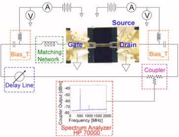
The FET device was based on the massive parallel nano-tube array techniques9–11and was nominally identical to the devices described recently.13 The dense arrays of single-walled nanotubes 共SWNTs兲 were grown by chemical vapor deposition on single crystal quartz substrates. The average density of the tubes was⬃5 SWNT/m with the local den-sity as high as⬃25 SWNT/m. The average length of the tubes was around 100 m. The device used split source and common drain electrodes with the gate electrode in a double finger configuration13as shown in Fig. 2 共center兲. The total
gate width 共W兲 was 300 m and the gate length 共Lg兲 was
4 m. The parasitic capacitances were reduced by lowering the overlap of gate and S/D electrodes. Double layer gate dielectric consisting of HfO2 共⬇10 nm兲, formed by atomic layer deposition, and benzocyclobutene共⬇20 nm兲 spin cast on the SWNTs was used. The capacitance of the bilayer di-electric is 共Cg兲⬇160 nF/cm2. The field effect mobility of
the device calculated using parallel plate capacitance for Vds
between −0.5 and −2 V is 150– 200 cm2/Vs. This value
was comparable to our previous reports of similar devices with similar channel lengths.10,11 The on/off ratio, on the other hand, was somewhat lower. This device showed pre-dominately p-channel behavior with gm⬇2.7 mS at a drain
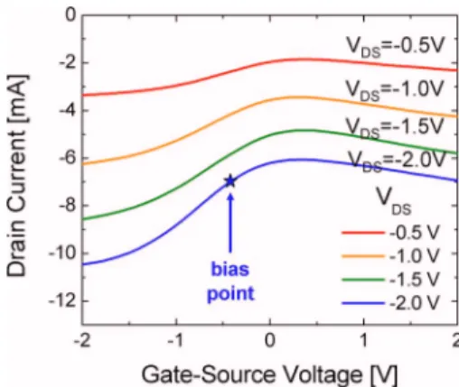
bias of −2 V and gate bias of −0.4 V 共Fig. 1兲. This
corre-sponded to an average transconductance/nanotube of ⬃1.8 S. The average on-current per nanotube was esti-mated to be ⬃5 A. Approximately one-third of the SWNTs in the channel were metallic, which resulted in a low ratio of on and off currents. The metallic SWNTs also limited the available gmR0 toⱕ2. From Fig.1, the measured gmR0
⬇1.15. Elimination of metallic nanotubes is a topic of cur-rent interest, and based on a simple model that assumes that the conductance of a metallic CNT and the transconductance of a semiconducting CNT are equal, gmR0⬇共1−␥兲/␥, where
␥ is the fraction of metallic CNTs in the array. Thus the fraction of metallic SWNTs must be reduced below⬃8% to realize gmR0⬎10 necessary for 20 dB of broadband gain.
Digital applications require significantly lower fractions of metallic SWNTs.
Large numbers of isolated SWNTs provide large values of transconductance without sacrificing the intrinsic perfor-mance of the tubes. This high transconductance with small parasitic capacitance leads to devices with good performance in the rf range. Although the gate-drain capacitance共Cgd兲 has not been calculated from the device geometry, the measured
Cgd was ⬇0.25 pF. The dependence of maximum gain on
a兲Electronic mail: [email protected].
FIG. 1. 共Color online兲 Measured CNT FET drain current with gate-source voltage with the drain source voltage as a parameter. The device operating point for the oscillator test was Vgs= 0.4 V and Vds= −2.0 V.
APPLIED PHYSICS LETTERS 93, 123506共2008兲
frequency derived from two port S-parameter data for iden-tical devices at frequencies between 10 MHz and 10 GHz, indicating a unity power gain共fmax兲 of 1 GHz, and additional
details of the rf device measurements were given previously.13
A schematic of the measurement system for an oscillator where the gain was provided by the CNT FET described above is shown in Fig.2. A series inductor at the gate of the FET enabled impedance matching. The inductor combined with the Cgd to form a resonator, stepping up the voltage on
the input to the gate. The inductor, estimated at 2 nH, was a short length of high impedance transmission line. In prin-ciple, the oscillation frequency is roughly set by the inductor/ gate-capacitance resonant frequency, which provides maxi-mum gain at that frequency, and is accurately adjusted to the desired frequency by the variable coaxial delay line, which sets the loop phase shift to 2nradians. However, in practice the conditions for oscillation were more complicated because the output of the CNT amplifier was not purely 50 ⍀ resis-tive and its complex impedance was presented to the resona-tor circuit by transformation through an arbitrary length of coaxial line that formed the feedback path. Figure 3 shows the oscillator output as a function of frequency with the fun-damental output at 500 MHz and harmonic outputs at 1000 and 1500 MHz. The measured power at the 500 MHz funda-mental was −40 dBm corresponding to a −20 dBm signal
level at the drain output of the FET. The relatively low out-put power compared to the FET dissipation of ⬃11.5 dBm was due to the presence of metallic nanotubes that increase the FET power dissipation without contributing to the gain and prevent effective impedance matching of the FET drain output.
The results presented here provide confirmation that CNT FETs can provide power gain in a 50 ⍀ circuit at uhf frequencies. Rapid progress toward broadband gain at micro-wave and millimeter-micro-wave frequencies is expected as device processing techniques are optimized for short gate length devices and metallic tubes are eliminated.
1J. E. Baumgardner, A. A. Pesetski, J. M. Murduck, J. X. Przybysz, J. D. Adam, and H. Zhang,Appl. Phys. Lett. 91, 052107共2007兲.
2D. V. Singh and K. A. Jenkins, Conference Digest, 62nd IEEE Device Research Conference共IEEE, New York, 2004兲, p. 53.
3S. Rosenblatt, H. Lin, V. Sazonova, S. Tiwari, and P. L. McEuen,Appl. Phys. Lett. 87, 153111共2005兲.
4A. A. Pesetski, J. E. Baumgardner, E. Folk, J. X. Przybysz, J. D. Adam, and H. Zhang,Appl. Phys. Lett. 88, 113103共2006兲.
5Z. Yu and P. J. Burke,Proc. SPIE 5790, 246共2005兲.
6S. Kim, T.-Y. Choi, L. Rabieirad, J.-H. Jeon, M. Shim, and S. Mohammadi, IEEE MTT-S International Symposium Digest共IEEE, New York, 2005兲, p. 303.
7J.-M. Bethoux, H. Happi, A. Siligaris, G. Dambrine, J. Borghetti, V. Derycke, and J.-P. Bourgoin, IEEE Trans. Nanotechnol. 5, 335共2006兲. 8J.-M. Bethoux, H. Happy, G. Dambrine, V. Derycke, M. Goffman, and
J.-P. Bourgoin,IEEE Electron Device Lett. 27, 681共2006兲.
9C. Kocabas, M. Shim, and J. A. Rogers,J. Am. Chem. Soc. 128, 4540 共2006兲.
10C. Kocabas, S. J. Kang, T. Ozel, M. Shim, and J. A. Rogers, J. Phys. Chem. C 111, 17879共2007兲.
11S. J. Kang, C. Kocabas, T. Ozel, M. Shim, N. Pimparkar, M. A. Alam, S. V. Rotkin, and J. A. Rogers,Nat. Nanotechnol. 2, 230共2007兲.
12D. Wang, Z. Yu, S. McKernan, and P. J. Burke, IEEE Trans. Nanotechnol.
6, 400共2007兲.
13C. Kocabas, H.-S. Kim, T. Banks, J. A. Rogers, A. A. Pesetski, J. E. Baumgardner, S. V. Krishnaswamy, and H. Zhang,Proc. Natl. Acad. Sci. U.S.A. 105, 1405共2008兲.
14Z. Chen, J. Appenzeller, Y.-M. Lin, J. Sippel-Oakley, A. G. Rinzler, J. Tang, S. J. Wind, P. M. Solomon, and P. Avouris, Science 311, 1735 共2006兲.
FIG. 2. 共Color online兲 Circuit schematic for the SWNT based 500 MHz oscillator. The SWNT FET is shown in the center of the figure and consists of a split source with two gate electrodes and a common drain. The gate is 300 m wide with a gate length of 4 m. The FET electrodes are con-tacted by coplanar probes. Bandpass gain at 500 MHz was provided by the matching network and the loop phase shift was set by the coaxial delay line. The coupling loss of the output coupler was 20 dB.
FIG. 3. 共Color online兲 CNT FET oscillator output power as a function of frequency measured on an HP 70000 Spectrum Analyzer.