Semiconductor Science and Technology
LETTER TO THE EDITOR
In-situ focused ion beam implantation for the
fabrication of a hot electron transistor oscillator
structure
To cite this article: I I Kaya et al 1996 Semicond. Sci. Technol. 11 L135
View the article online for updates and enhancements.
Related content
Hot electron spectroscopy and microscopy
J Smoliner, D Rakoczy and M Kast
-Resonant tunnelling of quasi-ballistic electrons in a hot electron transistor. Evidence for a breakdown of momentum conservation
V H Y Lam, M W Dellow, S J Bending et al.
-InP/InGaAs double-heterojunction bipolar transistor
Wen-Huei Chiou, Hsi-Jen Pan, Rong-Chau Liu et al.
-Recent citations
NONEQUILIBRIUM TRANSPORT AND THE BERNOULLI EFFECT OF ELECTRONS IN A TWO-DIMENSIONAL ELECTRON GAS
SMET . KAYA
-Electron-avalanche amplifier based on the electronic Venturi effect
D. Taubert et al
-Absolute Negative Resistance Induced by Directional Electron-Electron Scattering in a Two-Dimensional Electron Gas
Ismet I. Kaya and Karl Eberl
Semicond. Sci. Technol. 11 (1996) 135–138. Printed in the UK
LETTER TO THE EDITOR
In-situ
focused ion beam implantation
for the fabrication of a hot electron
transistor oscillator structure
I I Kaya†‡, M W Dellow†, S J Bending†, E H Linfield§, P D Rose§, D A Ritchie§and G A C Jones§
†School of Physics, University of Bath, Claverton Down, Bath BA2 7AY, UK
§Cavendish Laboratory, University of Cambridge, Madingley Road, Cambridge CB3 0HE, UK
Received 16 October 1995, accepted for publication 30 October 1995
Abstract. Recent advances usingin situfocused ion beam implantation during an MBE growth interruption have been exploited to fabricate planar GaAs hot electron structures without the need for shallow ohmic contacts. This novel fabrication route shows a very high yield and has been used to demonstrate a prototype
high-frequency oscillator structure based on electron multiplication in the base layer. Existing devices show transfer factors in excess of unity as well as reversal of the base current at high injection levels, which are the prerequisites for oscillator action. Future improvements in device design are discussed.
Over the last 10 years considerable interest has been shown in planar transistor structures based on the ballistic transport of carriers across a narrow base electrode [1, 2]. Due to the very low ballistic transit times through such devices (∼ 100 fs) they have great potential as high-frequency current amplifiers and rapidly switching logic elements, possibly into the THz regime. A major stumbling block in the development of such devices, however, has been the need to make reproducible shallow ohmic contacts to the very thin (∼ 50 nm) buried base electrode without shorting through the narrow (∼ 100 nm) tunnel barrier to the collector electrode below. We demonstrate here a fabrication route based on in situ focused ion beam implantation [3] which completely eliminates the need for shallow base ohmic contacts and leads to a very high yield of working transistors. Furthermore we use this fabrication route for the first time to demonstrate a prototype high-frequency oscillator structure based on electron multiplication in the base layer of a tunnelling hot electron transfer amplifier (THETA).
Reports by Brill and Heiblum [4] of electron multiplication in a THETA device with a very low collector barrier led us to the recent proposal of a very high frequency oscillator based on this effect [5]. In this structure electrons are tunnel injected at high energy into a very narrow n+ -GaAs base layer. If the transistor is ‘on’, most of these electrons pass to the collector electrode over a second wider tunnel barrier without significant loss of energy. Brill and
‡ Also at the Department of Physics, Bilkent University, 06533 Ankara,
Turkey.
Heiblum were, however, able to show that a substantial fraction of hot electrons share some of their energy with the thermalized dopant electrons in the base region, which can in turn be excited over the collector barrier if it is low enough. Consequently it is possible for the collector current to exceed the injected emitter current (i.e.α = IC/IE> 1) at which point the base–emitter junction shows regions of negative differential and absolute resistance. This junction can be made to oscillate at very high frequencies in an appropriate resonant circuit and the signal delivered with gain to a load at the collector.
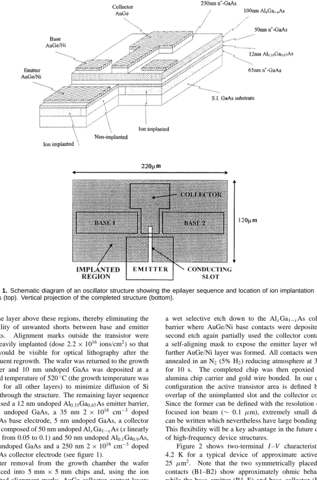
The use of in situ focused ion beam implantation allows us to reverse the epilayer sequence which would conventionally be chosen with a shallow ohmic contact technology. A schematic diagram of the MBE-grown GaAs/AlGaAs transistor is shown in figure 1. The structure is formed by growing a 500 nm undoped GaAs buffer layer followed by a 65 nm 3×1018cm−3Si-doped GaAs emitter electrode on top of a semi-insulating GaAs substrate. After a further 10 nm 1× 1017 cm−3 doped n+-GaAs cap layer had been added, the growth was interrupted and the wafer moved under ultra high vacuum into a separate chamber for focused ion beam implantation. Large rectangular-shaped regions of the emitter electrode, beneath where the base ohmic contacts would be formed, were implanted with 30 keV Ga ions at a dose of 1.0 × 10¹⁴ ions/cm2, except for a small unimplanted slot in the middle which forms both the emitter contact and active device region. The ion implanted emitter regions become highly resistive [3] and deep ohmic contacts were subsequently made to
Letter to the Editor
Figure 1. Schematic diagram of an oscillator structure showing the epilayer sequence and location of ion implantation regions (top). Vertical projection of the completed structure (bottom).
the base layer above these regions, thereby eliminating the possibility of unwanted shorts between base and emitter contacts. Alignment marks outside the transistor were very heavily implanted (dose 2.2 × 10¹⁶ ions/cm2) so that they would be visible for optical lithography after the subsequent regrowth. The wafer was returned to the growth chamber and 10 nm undoped GaAs was deposited at a reduced temperature of 520◦C (the growth temperature was 590◦C for all other layers) to minimize diffusion of Si atoms through the structure. The remaining layer sequence comprised a 12 nm undoped Al0.33Ga0.67As emitter barrier,
10 nm undoped GaAs, a 35 nm 2× 1018 cm−3 doped n+-GaAs base electrode, 5 nm undoped GaAs, a collector barrier composed of 50 nm undoped AlxGa1−xAs (x linearly
graded from 0.05 to 0.1) and 50 nm undoped Al0.1Ga0.9As, 5 nm undoped GaAs and a 250 nm 2× 1018cm−3 doped n+-GaAs collector electrode (see figure 1).
After removal from the growth chamber the wafer was diced into 5 mm× 5 mm chips and, using the ion implanted alignment marks, AuGe collector contact layers were thermally evaporated onto the individual samples. The collector contacts were then used as etch masks in
a wet selective etch down to the AlxGa1−xAs collector barrier where AuGe/Ni base contacts were deposited. A second etch again partially used the collector contact as a self-aligning mask to expose the emitter layer where a further AuGe/Ni layer was formed. All contacts were then annealed in an N2 (5% H2) reducing atmosphere at 380◦C for 10 s. The completed chip was then epoxied to an alumina chip carrier and gold wire bonded. In our device configuration the active transistor area is defined by the overlap of the unimplanted slot and the collector contact. Since the former can be defined with the resolution of the focused ion beam (∼ 0.1 µm), extremely small devices can be written which nevertheless have large bonding pads. This flexibility will be a key advantage in the future design of high-frequency device structures.
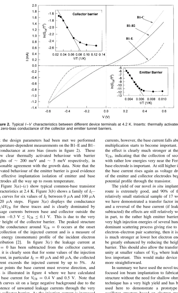
Figure 2 shows two-terminal I–V characteristics at 4.2 K for a typical device of approximate active area 25 µm2. Note that the two symmetrically placed base contacts (B1–B2) show approximately ohmic behaviour, while the base–emitter (B1–E) and base–collector (B1–C) characteristics are strongly nonlinear and indicate the tunnel transport that we would expect. To check 136
Letter to the Editor
Figure 2. TypicalI–V characteristics between different device terminals at 4.2 K. Inserts: thermally activated behaviour of the zero-bias conductance of the collector and emitter tunnel barriers.
that the design parameters had been met we performed temperature-dependent measurements on the B1–E and B1– C conductance at zero bias (insets in figure 2). These show clear thermally activated behaviour with barrier heights of ∼ 200 meV and ∼ 5 meV respectively, in reasonable agreement with the growth data. Note that the activated behaviour of the emitter barrier is good evidence for effective implantation isolation of emitter and base electrodes all the way up to room temperature.
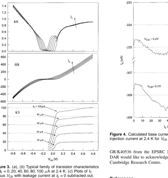
Figure 3(a)–(c) show typical common-base transistor characteristics at 2.4 K. Figure 3(b) shows a family ofIC–
VCBcurves for six values ofIEbetween 0µA and 100 µA in 20 µA steps. Figure 3(a) displays the conductance dIC/dVCB for these traces and is clearly dominated by leakage currents between base and collector outside the region −0.3 V ≤ VCB ≤ 0.1 V. This is due to the very low height of the collector barrier. The peaked structure in the conductance around VCB = 0 occurs at the onset of collection of the injected current and is a measure of the energy (momentum) profile of the incident electron distribution [2]. In figure 3(c) the leakage current at IE = 0 has been subtracted from the collector current, and it is clearly seen that for some values of the injection current, in particularIE= 40 µA and 60 µA, the collected current exceeds the injected current by up to 5%. At these points the base current must reverse direction, and this is illustrated in figure 4 where we have calculated the base current for VCB = 0.4 V and 0.5 V. Note that both curves sit on a large negative background due to the existence of unwanted leakage currents through the very low collector barrier. As the injection current is increased from zero the base current initially increases as electrons relax and become trapped in the base region. At larger
currents, however, the base current falls abruptly as electron multiplication starts to become important. The strength of the effect is clearly much stronger at the larger value of VCB, indicating that the collection of secondary electrons with rather low energies very near the Fermi energy of the base electrode is important. At still higher injection currents the base current rises again as voltage drops in the plane of the emitter and collector electrodes begin to distort the potential profile through the transistor.
The yield of our novel in situ implantation fabrication route is extremely good, and 90% of the devices in a relatively small statistical sample of 17 worked. Although we have demonstrated a transfer factor in excess of unity and a reversal of the base current (if leakage currents are subtracted) the effects are still relatively weak. This is due, in part, to the rather high emitter barrier which leads to very high injection energies of several hundred meV. If the dominant scattering process giving rise to multiplication is electron–electron pair scattering, then it is known that this is much stronger at lower hot electron energies and could be greatly enhanced by reducing the height of the emitter barrier. This should also allow the transfer factor to exceed unity at smaller values ofVCB where leakage currents are less important. This would make device diagnosis much more straightforward.
In summary we have used the novel technique of in situ focused ion beam implantation to fabricate a hot electron structure without the need for shallow ohmic contacts. The technique has a very high yield and has been successfully used here to demonstrate a prototype high-frequency oscillator structure based on electron multiplication in a THETA device. The prerequisites for oscillation, namely a transfer factor in excess of unity and reversal of the base
Letter to the Editor
Figure 3. (a), (b) Typical family of transistor characteristics forIE= 0,20,40,60,80,100µA at 2.4 K. (c) Plots ofIC
versusVCBwith leakage current atIE= 0 subtracted out.
current, have been demonstrated and simple improvements, that should lead to much better figures of merit, proposed. We note that our fabrication route can be used with any planar transistor structure, and the observed high device yields could well lead to a renaissance in interest in planar hot electron devices.
This work was supported in part by grant number
Figure 4. Calculated base current as a function of emitter injection current at 2.4 K forVCB= 0.4 and 0.5 V.
GR/K40536 from the EPSRC Nanotechnology Initiative. DAR would like to acknowledge support from the Toshiba Cambridge Research Centre.
References
[1] Hayes J R, Levi A F J and Wiegmann W 1985 Phys. Rev. Lett. 54 1570
[2] Heiblum M, Nathan M I, Thomas D C and Knoedler C 1985 Phys. Rev. Lett. 55 2200
[3] Linfield E H, Jones G A C, Ritchie D A and Thompson J H 1993 Semicond. Sci. Technol. 8 415
[4] Brill B and Heiblum M 1994 Phys. Rev. B 49 14 762 [5] Dellow M W, Cronin N J and Bending S J 1994 Appl.
Phys. Lett. 65 2463