High-performance visible-blind GaN-based
photodetectors
Bayram Butun, Turgut Tut, Erkin Ulker, Tolga Yelboga, and Ekmel Ozbay
Citation: Appl. Phys. Lett. 92, 033507 (2008); doi: 10.1063/1.2837645 View online: http://dx.doi.org/10.1063/1.2837645
View Table of Contents: http://aip.scitation.org/toc/apl/92/3
Published by the American Institute of Physics
Articles you may be interested in
Low-noise GaN ultraviolet photodiodes on GaN substrates
Applied Physics Letters 94, 221109 (2009); 10.1063/1.3148812
High speed, low noise ultraviolet photodetectors based on GaN and structures
Applied Physics Letters 71, 2154 (1998); 10.1063/1.119366
Semiconductor ultraviolet detectors
Journal of Applied Physics 79, 7433 (1998); 10.1063/1.362677
Fabrications and application of single crystalline GaN for high-performance deep UV photodetectors
AIP Advances 6, 085117 (2016); 10.1063/1.4961878
Fabrication of non-polar GaN based highly responsive and fast UV photodetector
Applied Physics Letters 110, 103507 (2017); 10.1063/1.4978427
High-performance (Al,Ga)N-based solar-blind ultraviolet p–i–n detectors on laterally epitaxially overgrown GaN
High-performance visible-blind GaN-based p-i-n photodetectors
Bayram Butun,a兲 Turgut Tut, Erkin Ulker, Tolga Yelboga, and Ekmel Ozbay
Nanotechnology Research Center, Department of Physics, and Department of Electrical and Electronics Engineering, Bilkent University, Bilkent, 06800 Ankara, Turkey
共Received 28 November 2007; accepted 21 December 2007; published online 24 January 2008兲 We report high performance visible-blind GaN-based p-i-n photodetectors grown by metal-organic chemical vapor deposition on c-plane sapphire substrates. The dark current of the 200m diameter devices was measured to be lower than 20 pA for bias voltages up to 5 V. The breakdown voltages were higher than 120 V. The responsivity of the photodetectors was ⬃0.23 A/W at 356 nm under 5 V bias. The ultraviolet-visible rejection ratio was 6.7⫻103 for wavelengths longer than 400 nm. © 2008 American Institute of Physics.关DOI:10.1063/1.2837645兴
The recent developments in high quality GaN/AlGaN material growth technology have led to the realization of high performance solar/visible-blind photodetectors operat-ing in the ultraviolet共UV兲 spectral region. Some applications in which GaN/AlGaN-based photodetectors are utilized in-clude engine/flame monitoring and detection, plant/ vegetation growth monitoring, UV astronomy, and gas detection.1–6 These photodetectors are also chemically inert and suitable for harsh environments. GaN-based solid-state photodetectors with breakdown voltages of⬃100 V,7–9 re-sponsivities of 0.18 A/W at 360 nm 共Ref.10兲 共for Schottky
type photodetectors兲 and 0.2 A/W at 355 nm 共for back illu-minated GaN based p-i-n photodetectors兲 which correspond to 70% quantum efficiency at zero bias,113 dB bandwidth of 16 GHz共for MSM type photodetectors兲12 and 1.6 GHz共for
p-i-n type photodetectors兲13 have been previously reported. In this paper, we report our experimental results on high performance GaN photodetectors. Our GaN photodetectors have higher breakdown voltage, lower current density, and higher responsivity when compared to the previously pub-lished GaN photodetector results in the literature.
The GaN p-i-n structure used in the present study was grown on double-side polished c-plane sapphire 共Al2O3兲
substrates by low-pressure metal organic chemical vapor deposition共MOCVD兲 system, which is located at the Bilkent University Nanotechnology Research Center. First, the wafer surface was cleaned by desorption in an H2 environment at 1080 ° C. Then, ⬃1000 Å AlN nucleation layer was grown at 500 ° C by trimethylaluminum 共TMAl兲 and ammonia 共NH3兲. The wafer surface was recrystallized by annealing at
970 ° C. After recrystallization, a high temperature GaN buffer layer of 2500 Å was grown with trimethylgallium 共TMGa兲 and high flow NH3 at 1160 ° C. A n layer with a
thickness of 5000 Å was grown with silane共SiH4兲, in turn,
resulting in a carrier concentration of 1018cm−3. The growth
continued with a 5000 Å i layer. In the last step, an 800 Å p layer with Mg doping by biscyclopentadienylmagnesium 共Cp2Mg兲 was grown.14,15 In all of the steps, the carrier gas
was H2and the chamber pressure was kept at 200 mbars.
The samples were fabricated by a six-step microwave-compatible fabrication process16–18 in class-100 clean room environment. The dry etching was accomplished by reactive
ion etching共RIE兲 under CCl2F2 plasma, 20 SCCM共SCCM
denotes cubic centimeter per minute at STP兲 gas flow rate, and 200 W rf power conditions. Mesa structures of the de-vices were formed via the RIE process by etching all of the layers共⬎1.2m兲 down to the nucleation layer for mesa iso-lation. After an Ohmic etch of ⬃0.74m, Ti/Al 共100 Å/1000 Å兲 contacts and Ni/Au 共100 Å/1000 Å兲 con-tacts were deposited by thermal evaporation and left in ac-etone for the lift-off process. The Ohmic contacts were an-nealed at 750 ° C for 45 s. Thereafter, a 300 nm thick Si3N4
was deposited via plasma enhanced chemical vapor deposi-tion for passivadeposi-tion. Finally, an⬃0.4m thick Ti/Au inter-connect metal was deposited and lifted-off in order to con-nect the n-type and p-type Ohmic contact layers to the coplanar waveguide transmission line pads.
For the present study, current-voltage 共IV兲, quantum ef-ficiency 共QE兲, capacitance-voltage 共CV兲, and high speed measurements were performed. IV characterization of the fabricated photodetectors was carried out by using a Keithley 6517A high resistance electrometer with low noise triax cables. QE measurements were performed using a xenon arc lamp, monochromator, UV-enhanced fiber, and SRS lock-in amplifier. The capacitances of diodes were measured by an Agilent 4980A LCR meter. The consistency of the measured current levels, in the dark and illuminated cases, was con-firmed by all the three current measurement made by these different experimental setups.
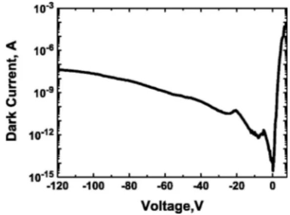
The IV measurement results in Fig.1show that the zero bias dark current of a 200m diameter photodetector was
a兲Author to whom correspondence should be addressed. Electronic mail:
FIG. 1. Current voltage measurements of a photodetector with a 200m diameter.
APPLIED PHYSICS LETTERS 92, 033507共2008兲
14 fA, and with corresponding current density of 44 pA/cm2. This current level corresponds to the
back-ground noise floor of the electrometer used for the experi-ments. At 1 V reverse bias, the dark current of the device was 20 fA and at 5 V it was 1.6 pA. The breakdown volt-ages of the photodetectors were measured to be higher than 120 V.
The turn-on voltage of the fabricated device was around 3 V. The current level of the device for biases below 0.2 V was below the measurement limit. Therefore, a linear fit to the IV curve of the device was made for bias values from 0.2 to 0.7 V. Using this linear fit, the ideality factor of the photodiode was calculated as n = 1.97. The contact resis-tances were 0.75 k⍀ for n-type contacts and 15.0 k⍀ for
p-contacts with 100⫻200m2contact pads.
We measured responsivity of 100m diameter diodes for bias voltages up to 30 V and observed a maximum UV-visible rejection ratio of 6.7⫻103 for wavelengths longer
than 400 nm 共Fig. 2兲. Responsivity at 358 nm was 0.20,
which corresponds to 70% quantum efficiency. For wave-lengths below 360 nm, the responsivity of the devices did not significantly change with applied reverse bias voltages larger than 5 V. Apparently, the diodes were depleted for small voltages, and to confirm this effect we performed CV measurements of the fabricated devices.
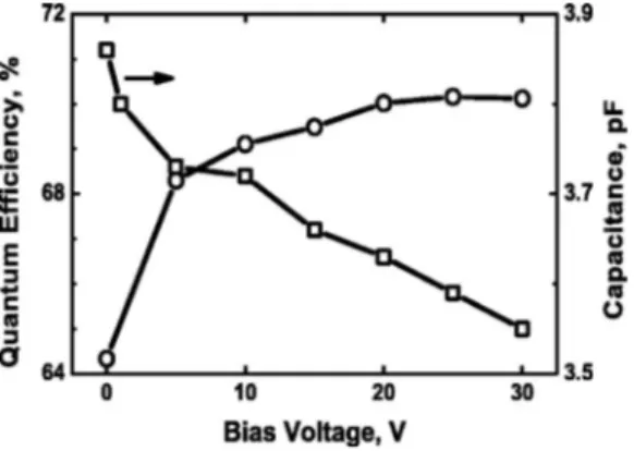
Figure3shows the QE 共at 358 nm兲 and the capacitance measurements of a 100m diameter device as a function of applied reverse bias. The QE quickly increased from 64% at 0 V reverse bias to 68% at 5 V reverse bias. For applied reverse biases larger than 5 V, the QE stayed almost constant
with a maximum of 70% at 30 V applied reverse bias. The capacitance of the 100m diameter device also had a simi-lar dependency on applied reverse bias. The capacitance quickly dropped from 3.86 pF at 0 V applied reverse bias to 3.7 pF at 5 V applied reverse bias. Afterwards, the capaci-tance of the device slowly decreased to 3.55 pF as the re-verse bias voltage was changed to 30 V. These data clearly showed that most of the intrinsic region was already depleted at very low voltages.
Figure4shows that the peak QE of the fabricated device was at 300 nm under 5 V bias. This was in contradiction with the normally expected peak wavelength of 360 nm due to the band gap of GaN. This shift in peak QE wavelength can be explained with the additional optical phase coming from the finite thickness of the deposited dielectric layer. A similar shift was also observed in transfer matrix method 共TMM兲 simulations of the QE for devices with varying top dielectric thicknesses. In order to confirm this explanation by experiments, the top Si3N4 layer was etched with diluted HF : H2O关⬃3:500 共ml兲兴 solution in 20 nm. Figure4 shows
the QE measurements after 0, 20, and 40 nm recess etch of the top dielectric film. After a total etch of 40 nm, the peak QE was measured to be 80.1%, while the peak responsivity was 0.23 A/W under 5 V bias at 356 nm. To our knowledge, the 0.23 A/W responsivity value corresponds to the highest responsivity for the front illuminated GaN based p-i-n pho-todetectors reported in the scientific literature.
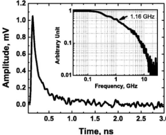
Using an ultrafast mode-locked fiber laser module with output pulses at 266 nm and 10 ps FWHM共full width at half maximum兲, we performed the high speed measurement of fabricated p-i-n photodiodes. Figure 5 shows the temporal pulse response and the FFT共fast Fourier transform兲 of the
p-i-n photodetectors. We measured 48 ps rise time, 351 ps
fall time, and 109 ps FWHM from a 100m diameter de-vice under 5 V reverse bias voltage. From the FFT data, the corresponding 3 dB bandwidth was found to be 1.16 GHz. This performance is close to the best 3 dB bandwidth of 1.6 GHz reported in the literature for GaN-based p-i-n photodetectors.11
In conclusion, we report the growth, fabrication, and characterization of high performance GaN-based p-i-n pho-todetectors. The optimized MOCVD growth conditions re-sulted in epitaxial samples that yielded high performance devices. A maximum 80.1% QE corresponding to 0.23 A/W responsivity at 356 nm, was achieved. The dark current of a
FIG. 2. Responsivity of a 100m diameter photodetector for different re-verse bias voltages.
FIG. 3. Voltage dependence of the quantum efficiency and capacitance for 100m diode.
FIG. 4. Spectral quantum efficiency of the photodetector after 0, 20, and 40 nm recess etch of the top dielectric film.
200m diameter circular diodes was measured to be 14 fA, along with a breakdown voltage larger than 120 V. To our knowledge, in terms of breakdown voltage, current density, and responsivity, the reported results are better than the pre-viously published GaN photodetector results in the scientific literature.
This work is supported by the European Union under the projects EU-NoE-METAMORPHOSE, EU-NoE-PHOREMOST, EU-PHOME, EU-ECONAM, and TUBI-TAK under Projects Nos. 105E066, 105A005, 106E198, 106A017, and 107A012. One of the authors共E.O.兲 also ac-knowledges partial support from the Turkish Academy of Sciences.
1M. Razeghi and A. Rogalski, J. Appl. Phys. 79, 7433共1996兲.
2E. Ozbay, N. Biyikli, I. Kimukin, T. Tut, T. Kartaloglu, and O. Aytur,
IEEE J. Quantum Electron. 10, 742共2004兲.
3S. J. Pearton, J. C. Zolper, R. J. Shul, and F. Ren, J. Appl. Phys. 86, 1
共1999兲.
4J. C. Campbell, S. Demiguel, F. Ma, A. Beck, X. Guo, S. Wang, X. Zheng,
X. Li, J. D. Beck, M. A. Kinch, A. Huntington, L. A. Coldren, J. Decobert, and N. Tscherptner, IEEE J. Quantum Electron. 10, 777共2004兲.
5N. Biyikli, I. Kimukin, T. Tut, O. Aytur, and E. Ozbay, Appl. Phys. Lett.
81, 3272共2002兲.
6N. Biyikli, I. Kimukin, O. Aytur, M. Gokkavas, M. S. Unlu, and E. Ozbay,
Appl. Phys. Lett. 79, 2838共2001兲.
7J. B. Limb, D. Yoo, J. H. Ryou, W. Lee, S. C. Shen, R. D. Dupuis, M. L.
Reed, C. J. Collins, M. Wraback, D. Hanser, E. Preble, N. M. Williams, and K. Evans, Appl. Phys. Lett. 89, 011112共2006兲.
8B. Yang, T. Li, K. Heng, C. Collins, S. Wang, J. C. Carrano, R. D. Dupuis,
J. C. Campbell, M. J. Schurman, and I. T. Ferguson, IEEE J. Quantum Electron. 36, 1389共2000兲.
9K. A. McIntosh, R. J. Molnar, L. J. Mahoney, K. M. Molvar, N. Efremov,
and S. Verghese, Appl. Phys. Lett. 76, 3938共2000兲.
10Q. Chen, J. W. Yang, A. Osinsky, S. Gangopadhyay, B. Lim, M. Z.
Anwar, M. Asif Khan, D. Kuksenkov, and H. Temkin, Appl. Phys. Lett.
70, 2277共1997兲.
11W. Yang, T. Nohova, S. Krishnankutty, R. Torreano, S. McPherson, and H.
Marsh, Appl. Phys. Lett. 73, 1086共1998兲.
12J. C. Carrano, T. Li, D. L. Brown, P. A. Grudowski, C. J. Eiting, R. D.
Dupuis, and J. C. Campbell, Appl. Phys. Lett. 73, 2405共1998兲.
13J. C. Carrano, T. Li, D. L. Brown, P. A. Grudowski, C. J. Eiting, R. D.
Dupuis, and J. C. Campbell, Electron. Lett. 34, 1779共1998兲.
14H. Yu, M. K. Ozturk, S. Ozcelik, and E. Ozbay, J. Cryst. Growth 293, 273
共2006兲.
15H. Yu, W. Strupinski, S. Butun, and E. Ozbay, Phys. Status Solidi A 203,
868共2006兲.
16N. Biyikli, I. Kimukin, T. Tut, T. Kartaloglu, O. Aytur, and E. Ozbay,
Semicond. Sci. Technol. 19, 1259共2004兲.
17N. Biyikli, I. Kimukin, O. Aytur, and E. Ozbay, IEEE Photonics Technol.
Lett. 16, 1718共2004兲.
18B. Butun, N. Biyikli, I. Kimukin, O. Aytur, and E. Ozbay, Appl. Phys.
Lett. 84, 4185共2004兲. FIG. 5. Temporal pulse response of the 100m micron diameter p-i-n
photodiodes under 5 V reverse bias voltage and the corresponding fre-quency response共inset兲.