OPTIMIZATION OF COUPLED CLASS-E RF
POWER AMPLIFIERS FOR A TRANSMIT
ARRAY SYSTEM IN 1.5T MRI
a thesis submitted to
the graduate school of engineering and science
of bilkent university
in partial fulfillment of the requirements for
the degree of
master of science
in
electrical and electronics engineering
By
Muhammed Said Aldemir
January 2020
OPTIMIZATION OF COUPLED CLASS-E RF POWER AMPLI-FIERS FOR A TRANSMIT ARRAY SYSTEM IN 1.5T MRI
By Muhammed Said Aldemir January 2020
We certify that we have read this thesis and that in our opinion it is fully adequate, in scope and in quality, as a thesis for the degree of Master of Science.
Ergin Atalar(Advisor)
Erdin¸c Tatar
Ali Bozbey
Approved for the Graduate School of Engineering and Science:
ABSTRACT
OPTIMIZATION OF COUPLED CLASS-E RF POWER
AMPLIFIERS FOR A TRANSMIT ARRAY SYSTEM IN
1.5T MRI
Muhammed Said Aldemir
M.S. in Electrical and Electronics Engineering Advisor: Ergin Atalar
January 2020
Radio Frequency (RF) field is generated mostly by linear RF power amplifiers in Magnetic Resonance Imaging (MRI). These amplifiers have relatively low effi-ciency and are placed far from the transmit coil in MRI system room. Additional cooling systems and long transmission cables increase the cost of MRI hardware. Coupled Class-E on-coil RF amplifiers for a Transmit Array System is proposed instead of linear RF amplifiers. Class-E RF amplifier is a nonlinear switching amplifier which has 100% drain efficiency ideally. State-space models for single Class-E amplifier and coupled Class-E amplifiers are derived and steady-state operation of coupled Class-E amplifiers is investigated. The state-space models are verified with the simulation results of the Class-E amplifier. Effect of cou-pling between channels on the output characteristics of the transmit system is observed.
Instead of implementing decoupling methods, coupling is maintained and op-timization of circuit parameters for coupled Class-E amplifiers is proposed to achieve high drain efficiency and high output RF power. Output power of 600 W and overall drain efficiency higher than 90% are achieved by two coupled Class-E amplifiers even with high coupling levels in the state-space model. Power and efficiency measurements are done with coupled amplifiers and MRI experiments are performed in 1.5T Scimedix MRI Scanner. In conclusion, coupled Class-E RF power amplifiers can be operated as on-coil amplifiers in a Transmit Array system with high output characteristics by optimization of circuit parameters.
¨
OZET
KUPLAJLI E-SINIFI RF G ¨
UC
¸ Y ¨
UKSELTEC
¸ LER˙IN˙IN
1.5T MRG VER˙IC˙I D˙IZ˙IS˙I S˙ISTEM˙I ˙IC
¸ ˙IN
OPT˙IM˙IZASYONU
Muhammed Said Aldemir
Elektrik ve Elektronik M¨uhendisli˘gi, Y¨uksek Lisans Tez Danı¸smanı: Ergin Atalar
Ocak 2020
Manyetik Rezonans G¨or¨unt¨uleme (MRG) de, Radyo Frekans (RF) alanı genellikle do˘grusal RF g¨u¸c y¨ukselte¸cleriyle ¨uretilir. Bu y¨ukselte¸cler nispeten d¨u¸s¨uk ver-imlili˘ge sahiptir ve verici sargısından uzaktaki MRG sistem odasına yerle¸stirilirler. Ek so˘gutma sistemleri ve uzun iletim kabloları, MRG donanım maliyetini arttırmaktadır. Do˘grusal RF y¨ukselte¸cler yerine, verici dizisi sistemi i¸cin ku-plajlı E-sınıfı sargı ¨uzeri RF y¨ukselte¸cler ¨onerilmi¸stir. E-sınıfı RF y¨ukselteci, ideal durumda %100 verimlili˘ge sahip, anahtarlamalı, do˘grusal olmayan bir y¨ukselte¸ctir. ˙Ideal E-sınıfı y¨ukselte¸c ve kuplajlı E-sınıfı y¨ukselte¸cler i¸cin durum-uzay modeli olu¸sturuldu, kuplajlı E-sınıfı y¨ukselte¸clerin denge durumu i¸sleyi¸si incelendi. E-sınıfı y¨ukselte¸c sim¨ulasyonu ile durum-uzay modeli do˘grulandı. Kanallar arasındaki kuplajın, verici sisteminin ¸cıkı¸s karakteristi˘gi ¨uzerindeki etk-isi g¨ozlemlendi.
Dekuplaj y¨ontemlerini uygulamak yerine kuplaj durumu devam ettirilmi¸s, y¨uksek verimlilik ve y¨uksek RF ¸cıkı¸s g¨uc¨u elde etmek amacıyla kuplajlı E-sınıfı y¨ukselte¸clerin devre parametrelerinin optimize edilmesi ¨one s¨ur¨ulm¨u¸st¨ur. Durum-uzay modelinde, iki kuplajlı E-sınıfı y¨ukselte¸c kullanılarak 600 W ¸cıkı¸s g¨uc¨u ve %90’ın ¨uzerinde toplam verimlilik, y¨uksek kuplaj seviyelerinde bile ba¸sarılmı¸stır. G¨u¸c ve verimlilik ¨ol¸c¨umleri kuplajlı y¨ukselte¸cler ile yapılmı¸s ve MRG deney-leri, 1.5T Scimedix MRG tarayıcısında ger¸cekle¸stirilmi¸stir. Sonu¸c olarak, devre parametrelerinin optimizasyonu ile kuplajlı E-sınıfı RF y¨ukselte¸cleri, sargı ¨uzeri y¨ukselte¸cler olarak verici dizisi sistemi i¸cerisinde y¨uksek ¸cıkı¸s karakteristi˘gi ile ¸calı¸stırılabilmektedir.
Acknowledgement
Foremost, I would like to express my sincere gratitude to Prof. Dr. Ergin Atalar for all his guidance and effort through my study. I am very grateful to be a member of UMRAM family and our group.
I would also like to thank my valuable friends Mustafa Can Delikanlı, Cem Benar, U˘gur Yılmaz, Alireza Sadeghi-Tarakameh and Reza Babaloo.
Finally, I must express my very profound gratitude to my family and love of my life for their heartfelt support and affection throughout my life.
Contents
1 Introduction 1
2 Theory 4
2.1 Magnetic Resonance Imaging . . . 5
2.2 Operation of Class-E Amplifier . . . 6
2.3 The Model of Ideal Class-E Amplifier . . . 9
2.4 The Model of Coupled Class-E Amplifiers . . . 13
2.5 Efficiency Considerations and Coupling Coefficient in Coupled Sys-tems . . . 20
3 Methods 23 3.1 Simulation of Coupled Class-E Amplifiers . . . 23
3.2 Experimental Setup . . . 25
3.2.1 Lab Experiments and Tuning Procedure . . . 25
CONTENTS vii
4 Results 30
4.1 Single Class-E amplifier Results . . . 31
4.1.1 State-Space Model . . . 31
4.1.2 Circuit Simulation . . . 32
4.1.3 Tuning Capacitors . . . 34
4.1.4 Load Variations . . . 35
4.2 Coupled Class-E amplifiers . . . 38
4.2.1 State-Space Model . . . 38
4.2.2 Circuit Simulation . . . 41
4.2.3 Effect of Coupling . . . 44
4.2.4 Tuning Capacitors . . . 45
4.2.5 Effect of Amplitude and Phase Variation . . . 52
4.2.6 Load Variations . . . 57
4.3 Experimental Results . . . 60
4.3.1 Hardware Experiments . . . 61
4.3.2 MRI Experiments . . . 67
5 Discussion and Conclusion 72
List of Figures
2.1 Ideal Class-E amplifier circuit . . . 6 2.2 The switch voltage and current waveform respectively for Class-E
amplifier. . . 8 2.3 Coupled inductors and T model equivalent circuit for coupled
in-ductors . . . 13 2.4 Coupled Class-E amplifiers circuit . . . 14 2.5 Effect of adjusting load-network components on the voltage
wave-form of the switch[1] . . . 20
3.1 Power measurement setup diagram . . . 26 3.2 (a) Measurement setup for coupled Class-E amplifiers (b) Setup of
FPGA evaluation board and amplifier control part. . . 27 3.3 MRI experiment setup diagram . . . 29
4.1 Class-E amplifier steady state waveforms for load current IL1, series
capacitor voltage VC2, the choke inductor current ILch and the
LIST OF FIGURES ix
4.2 Circuit simulation parameters of Class-E amplifier . . . 32 4.3 Resulted waveforms of LTspice simulation for load current IL1,
series capacitor voltage VC2, the choke inductor current ILch and
the switch voltage VC1 respectively. . . 33
4.4 Drain Efficiency of the amplifier with respect to C1 and C2 . . . . 34
4.5 Output power of the amplifier with respect to C1 and C2 . . . 35
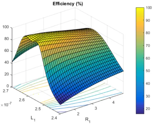
4.6 Drain Efficiency of the amplifier with respect to L1 and R1 . . . . 36
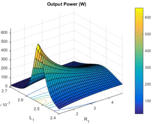
4.7 Output power of the amplifier with respect to L1 and R1 . . . 37
4.8 First channel’s steady state waveforms for load current IL1, series
capacitor voltage VC2, the choke inductor current ILch1 and the
switch voltage VC1 . . . 39
4.9 Second channel’s steady state waveforms for load current IL2, series
capacitor voltage VC4, the choke inductor current ILch2 and the
switch voltage VC3 . . . 40
4.10 LTspice simulation parameters of coupled Class-E amplifier . . . . 41 4.11 First amplifier’s simulation waveforms for load current IL1, series
capacitor voltage VC2, the choke inductor current ILch1 and the
switch voltage VC1 respectively. . . 42
4.12 Second amplifier’s simulation waveforms for load current IL2, series
capacitor voltage VC4, the choke inductor current ILch2 and the
switch voltage VC2 respectively. . . 43
4.13 Overall drain efficiency of coupled amplifiers versus varying cou-pling coefficient k. . . 44
LIST OF FIGURES x
4.14 Overall drain efficiency of coupled amplifiers versus varying series load capacitors when k=0.01. . . 47 4.15 Total output RF power versus varying series load capacitors when
k=0.01. . . 47 4.16 Power balance between amplifier channels when k=0.01. . . 48 4.17 Phase difference(◦) between the load currents of coupled amplifiers
when k=0.01. . . 48 4.18 Overall drain efficiency of coupled amplifiers versus varying series
load capacitors when k=0.10. . . 50 4.19 Total output RF power versus varying series load capacitors when
k=0.10. . . 50 4.20 Power balance between amplifier channels when k=0.10. . . 51 4.21 Phase difference(◦) between the load currents of coupled amplifiers
when k=0.10. . . 51 4.22 Overall drain efficiency versus supply voltage and phase of second
channel. . . 53 4.23 Total output power of coupled amplifiers versus supply voltage and
phase of second channel. . . 54 4.24 Power balance between the coupled amplifiers versus supply
volt-age and phase of second channel. . . 54 4.25 Overall drain efficiency versus supply voltage and phase of second
channel. . . 55 4.26 Total output power of coupled amplifiers versus supply voltage and
LIST OF FIGURES xi
4.27 Power balance between the coupled amplifiers versus supply volt-age and phase of second channel. . . 56 4.28 Drain efficiency of the coupled system with respect to L2 and R2 . 58
4.29 Total output power of coupled amplifiers with respect to L2 and R2 58
4.30 Power balance between amplifiers with respect to L2 and R2. . . . 59
4.31 Drain voltage waveform of the MOSFET when (a) There is no cou-pling between the amplifiers (b) Coucou-pling is introduced by bringing coils closer (c) Capacitors on the coil are tuned for coupled case. . 62 4.32 (a) Output voltage of the pick-up coil for 1st Class-E amplifier (b)
Output voltage of the pick-up coil for 2nd Class-E amplifier when amplifiers are working separately. . . 63 4.33 (a) Output voltage of the pick-up coil for 1st Class-E amplifier (b)
Output voltage of the pick-up coil for 2nd Class-E amplifier when the amplifiers are placed closer with a distance of 8cm. . . 64 4.34 After tuning the capacitors on the transmit coils (a) Output
volt-age of the pick-up coil for 1st Class-E amplifier (b) Output voltvolt-age of the pick-up coil for 2nd Class-E amplifier. . . 65 4.35 (a) MRI image of phantoms when two amplifiers are operating
simultaneously with a wide field of view (FOV) (b) MRI image of the same setup with decreased FOV. . . 67 4.36 Experimental setup for 3-channel coupled amplifiers . . . 68 4.37 MRI image of three phantoms while the amplifiers are working
simultaneously at 63.795 MHz. . . 68 4.38 4-channel transmit coil and placement of the amplifiers . . . 69
LIST OF FIGURES xii
4.39 Only (a) 1st channel is operating (b) 2nd channel is operating (c) 3rd channel is operating (d) 4th channel is operating . . . 70 4.40 (a) 2nd and 3rd amplifiers are working simultaneously with 10 V
supply voltage (b) the first three amplifiers are working simulta-neously with supply voltage of 28 V. . . 71
List of Tables
3.1 Data acquisition parameters of the MRI experiment . . . 28
4.1 Comparison of the amplifier model and the circuit simulation . . . 33 4.2 Comparison of the coupled amplifier model and the circuit
simu-lation when coupling between amplifiers is 10%. . . 41 4.3 Tuned new Cs values for each coupling degree and corresponding
drain efficiency and output power. . . 45 4.4 Some optimum points for the load capacitors and corresponding
output characteristics. . . 46 4.5 Some optimum points for the load capacitors and corresponding
output characteristics. . . 49 4.6 Measurement results of the amplifiers when there is no coupling. . 64 4.7 Measurement results of the amplifiers when a coupling is
intro-duced between the amplifiers. . . 65 4.8 Measurement results of the amplifiers when the load capacitors are
Chapter 1
Introduction
Magnetic Resonance Imaging (MRI) is a powerful medical imaging technique used for obtaining images of the human body. The hardware of MRI scanners consists of a magnet producing strong magnetic field that realigns protons in the body, a gradient amplifier, an Radio Frequency (RF) power amplifier, transmit and receive coils. The main function of the RF power amplifier is to generate RF pulses for the transmit coils. Conventional MRI scanners mostly use linear RF amplifiers which have relatively low efficiency due to the power loss during the transmission of the RF power from the MRI system room to RF coil. Additional cooling system and long transmission cables for the RF amplifier increases the cost of the system. The distance between the RF amplifier and the RF coil decreases the efficiency of the system.
As RF transmit coil, the birdcage coil design [2] is used in clinical MRI scan-ners commonly for a long time because of high B1 field homogeneity over a large
volume within the coil [3]. Then, parallel excitation method with an array of transmit coils for MRI is proposed [4]. Parallel excitation with a transmit ar-ray provides more degree of freedom, local excitation and shortened RF pulse duration [5]. Also, local specific absorption rate (SAR) reduction is achieved by parallel transmission with a coil array [6]. During the RF transmission, phase and amplitude of each coil element can be controlled independently in transmit
array systems. Several hardware implementations of parallel transmission with coil arrays is presented [7, 8, 9].
In literature, mostly linear RF amplifiers are used for parallel transmit arrays. There are quite few works which use Class-D RF amplifiers for the parallel trans-mission [10, 11]. Gudino implemented 4-channel on-coil transmit array for 7T MRI with current mode Class-D amplifiers which are controlled with a fiber op-tic cable. The output power level of the amplifiers is around 44 W. They achieved decoupling of transmit coils with isolation above 20 dB by the amplifier decou-pling method. Also, Twieg proposed an RF power amplifier module producing peak RF power up to 130 W with an overall efficiency of 85% for parallel transmit arrays at 3T. The design consists of current mode Class-D power amplifier [11].
The previous studies on the transmit array mainly concentrate on implement-ing coil system, amplifiers separately and they use decouplimplement-ing methods to decou-ple transmit coils on the transmit array. Then, it is shown that Class-E amplifier can be implemented as on-coil amplifiers for MRI transmit array system by the studies of our research group. Poni implemented a modified Class-E amplifier of 100 W output power for 3T with the drain efficiency up to 88% [12]. In that design, the coil element is considered as RLC network and 50 Ω matching is not re-quired for the load. By only adjusting the transmit coil components according to the system Larmor frequency, that Class-E amplifier design can be implemented for 1.5T and 3T MRI scanners. Then, Zahra proposed digitally controlled Class-E RF amplifier with supply modulation which has an output power of 300 W with maximum drain efficiency of 92% [13]. Also, a novel gate modulation technique is implemented for modified Class-E amplifier by Ashfaq [14].
In this work, the state-space model for the coupled Class-E amplifiers is pro-posed. By using the model, the operation and performance of Class-E amplifiers in a coupled system are investigated. Instead of applying decoupling methods to transmit coils in the array, coupling between the coils is maintained and optimiza-tion of the amplifier components is proposed in order to achieve high efficiency and output power for the coupled transmit channels in the array. Coupled Class-E amplifiers are modelled in a numerical computing environment and steady-state
solution is presented. Output characteristics of coupled amplifiers such as drain efficiency, output power, power balance between amplifiers and phase are studied for various circuit parameters. The effects of load variations, coupling, phase-amplitude variation on the coupled system’s output characteristics are investi-gated with the model. Optimum operating points ensuring high drain efficiency for coupled amplifiers are found and variation limits for several circuit parameters are discussed.
The main motivation of this study is to replace linear RF power amplifiers used in conventional MRI systems with highly efficient on-coil Class-E RF power am-plifiers. These amplifiers are designed to be used as elements of a Transmit Array System for MRI. In the array, there is a coupling effect among each transmit ele-ment depending on the distance between transmit channels. In RF applications, coupling effects are generally eliminated by implementing decoupling methods and using additional circuitry. However, the coupling effect between elements is maintained in this study and it is shown that by optimization of coupled Class-E RF amplifiers, they can operate with an overall drain efficiency of 90% even under extreme coupling levels. Thus, coupled Class-E RF amplifiers can be operated in a Transmit Array with high output characteristics by controlling the circuit parameters of coupled system.
The rest of this thesis includes four parts. In the second part, the model of single Class-E amplifier and coupled Class-E amplifiers are presented, the steady-state solution is explained in detail. Techniques used in analyzing the operation of coupled Class-E amplifiers and performing lab experiments are reported in the third section. In the fourth section, results of single Class-E amplifier and coupled amplifiers in the state-space model, simulations, lab experiments and MRI experiments are shown separately. In the final section, functionality of the model and experimental results are discussed.
Chapter 2
Theory
In this chapter, fundamentals of Magnetic Resonance Imaging is explained and operation of ideal Class-E RF power amplifier is described . A state-space model for ideal Class-E amplifier is presented. Class-E amplifier is a switching type amplifier and a gate driver signal turns on and off the switch of the amplifier consecutively. In order to model the Class-E amplifier, differential equations of the inductor’s current and the capacitor’s voltage are derived for both switch cases which the switch is on and the switch is off. By using initial conditions, the steady-state solution of these differential equations are acquired in a numerical computing environment. Then the model is expanded for coupled two class-E amplifiers. A mutual coupling is introduced between the load inductors of the amplifiers. The state-space representation of this coupled system is generated and solved by using the same method. With the amplifier model, voltage and current waveforms of the circuit elements can be plotted in the numerical computing environment and output characteristics of the amplifier such as drain efficiency, output power can be calculated. In order to verify the model, the Class-E amplifier is simulated in a circuit simulator and the waveforms are compared with simulation results in the circuit simulator.
2.1
Magnetic Resonance Imaging
Magnetic Resonance Imaging (MRI) is a noninvasive imaging technique used to acquire image of human body. Atoms which have odd number of protons like Hydrogen possess a net magnetic dipole moment when they are placed in a strong magnetic field. The total effect of magnetic dipole moments creates a net magnetization along the direction of the strong magnetic field. Nuclear spins show a resonance behaviour at a specific frequency which is called as Larmor frequency. Larmor frequency depends on two parameters : gyromagnetic ratio and magnetic field strength. For 1.5T MRI, the Larmor frequency of Hydrogen atom is 63.9 MHz.
There are three different magnetic fields in MRI. The first field is the main magnetic field B0. This strong magnetic field is generated by a superconducting
magnet in MRI scanner along z-direction. The produced magnetic field generates a net magnetization. The second magnetic field in MRI is the gradient field (G). This field can be produced along x, y and z-direction by separate gradient coils and gradient amplifier. Without the gradient field, the resonance frequency of atoms are same for different locations in the field of view. Presence of the gradi-ent field enables Larmor frequency of atoms to vary depending on the position, therefore spatial localization can be achieved in MRI by the gradient field. The third magnetic field in MRI is the Radio Frequency field B1. B1 field is applied
perpendicular to the main magnetic field. The functionality of the B1 field is to
excite spins and to change the direction of net magnetization vector. To achieve RF excitation in MRI, RF pulses at Larmor frequency should be applied by us-ing the transmit coils and the RF amplifier. After magnetization vector tipped into the transverse plane, transverse component of the magnetization precesses around B0. However, the magnetization vector returns to the equilibrium along
z-direction with a time constant of T1. Also, the transverse magnetization decays
with a time constant of T2. According to Faraday’s law of induction,
alternat-ing magnetic field of transverse component induces an electromotive force in the receive coil. The resultant time domain signal is called as free induction decay (FID). By reconstruction of the FID signal, MR image is acquired.
2.2
Operation of Class-E Amplifier
Class-E RF power amplifier is a nonlinear switching type amplifier which has 100% drain efficiency ideally. The ideal Class-E amplifier circuit is shown in Fig. 2.1. The Class-E amplifier consists of an ideal switch, a parallel capacitor C1, a resonant network L1 - C2, a load resistor R1 and a choke inductor Lch1. Lch1
is connected between the switch and the supply voltage. The switch is turned on and off periodically by a square wave signal called as switch drive signal. An RF load current generated across R1 by the Class-E amplifier.
Figure 2.1: Ideal Class-E amplifier circuit
For the lossless operation of Class-E amplifier two conditions should be satisfied: zero-voltage switching (ZVS) and zero-voltage derivative switching (ZVDS) [15]. The equations describing the operation of Class-E amplifier is derived [16, 17].
The current across the R1 is a sinusoidal signal :
When the switch is off, the current across C1 can be written as:
iC1(t) = ILch1(1 − αsin(wt + ϕ)) (2.2)
where αILch1= IR
The voltage across the switch can be written as:
VC1(t) =
ILch1
wC1
(wt + α(cos(wt + ϕ) − cos(ϕ))) (2.3)
Equations for the ZVS and ZVDS conditions can be written as follow:
VC1(t) t=T /2 = 0 (2.4) dVC1(t) dt t=T /2 = 0 (2.5)
After solving Eq. 2.3, α and ϕ can be found as:
α ≈ 1.86 and ϕ ≈ −32.48◦ (2.6) Then, we can write expressions for the switch voltage and the current across the switch over a period:
VC1(t) = ILch1 wC1 (wt + 1.86(cos(wt − 32.48 ◦) − 0.84))), 0 ≤ wt ≤ π 0, π ≤ wt ≤ 2π (2.7) Iswitch(t) = 0, 0 ≤ wt ≤ π I (1 − 1.86sin(wt − 32.48◦)), π ≤ wt ≤ 2π (2.8)
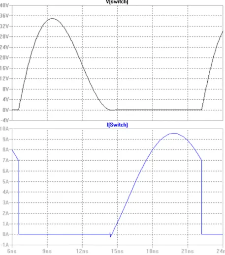
In Fig. 2.2, waveforms of the switch voltage and switch current are shown over a period. When the switch is off, the current passing the switch is zero. Similarly, the voltage on the switch is zero along a half period when the switch is on.
Figure 2.2: The switch voltage and current waveform respectively for Class-E amplifier.
2.3
The Model of Ideal Class-E Amplifier
In order to find a state-space model for ideal Class-E amplifier, the differential equations of the inductor current and the capacitor voltage are derived. The amplifier has two different states which are the switch is on state and off state. The state vector of the system can be defined as:
¯ x(t) = IL1(t) VC2(t) ILch1(t) VC1(t) (2.9)
The derived equations are in the form of first-order non-homogeneous differ-ential equations. The matrix differdiffer-ential equation can be written as :
d¯x(t) dt = ¯
¯
A¯x(t) − ¯b (2.10) where 0 ≤ t ≤ tlast
The state matrix A have different values when the switch is on and off there-fore the state matrices when the switch is off and on are named as ¯A¯1 and ¯A¯2
respectively. Also the state vectors are named as ¯x1 and ¯x2 for these cases. th is
defined as the half period of the switch drive signal.
The state space representation of the system when the switch is off;
d¯x1(t) dt = ¯ ¯ A1x¯1(t) − ¯b (2.11) where ¯A¯1 = −R L1 − 1 L1 0 1 L1 1 C2 0 0 0 0 0 0 − 1 Lch1 − 1 0 1 0 , ¯b = 0 0 −Vdd Lch1 0 and 0 ≤ t ≤ th
The state space representation of the system when the switch is on; d¯x2(t) dt = ¯ ¯ A2x¯2(t) − ¯b (2.12) where ¯A¯2 = −R L1 − 1 L1 0 0 1 C2 0 0 0 0 0 0 0 0 0 0 0 , ¯b = 0 0 −Vdd Lch1 0 and 0 ≤ t ≤ th
After powering this nonlinear amplifier, it takes some time to reach steady state. Simulating such a single Class-E amplifier requires several minutes at least depending on simulation parameters. Also tuning procedure of the amplifier requires significant amount of time, especially finding optimum capacitor values for tuning procedure of coupled Class-E amplifiers in a circuit simulator may last several hours. By using this model and coupled Class-E amplifier model, steady state waveforms can be generated and optimum capacitor values can be found in seconds in a numerical computing environment, therefore it is important to have such a model in order to understand the behaviour of coupled nonlinear amplifiers.
After reaching the steady state, voltage and current waveforms repeat them-selves at that frequency for switch is on and switch is off states. The final value of a state will be initial condition for the successive state, therefore the value of the state vector ¯x at t = th will be the initial condition of the second matrix
differential equation.
The solution of matrix differential equation in Eq. 2.10 can be written as:
¯
x(t) = eAt¯¯x0+ ¯A¯−1(I − e ¯ ¯
At)¯b (2.13)
eAt¯¯ = ∞ X n=1 tn n! ¯ ¯ An = I + t 1! ¯ ¯ A + t 2 2! ¯ ¯ A2+ t 3 3! ¯ ¯ A3+ ... + t k k! ¯ ¯ Ak+ ... (2.14) The solution is written for the switch is off and on case:
¯ x1(t) = ¯F¯1(t)¯x10+ ¯q1(t) (2.15) ¯ x2(t) = ¯F¯2(t)¯x20+ ¯q2(t) (2.16) where ¯F¯1(t) = e ¯ ¯ A1t and ¯F¯ 2(t) = e ¯ ¯ A2t ¯ q1(t) = ¯A¯−11 (I − e ¯ ¯ A1t)¯b (2.17) ¯ q2(t) = ¯A¯−12 (I − e ¯ ¯ A2t)¯b (2.18)
In order to find initial condition of each state, we can equate them to final value of the previous state :
¯ x10 = ¯x1(0) = ¯x2(th) = e ¯ ¯ A2thx¯ 20+ ¯A¯−12 (I − e ¯ ¯ A2th)¯b (2.19) ¯ x20 = ¯x2(0) = ¯x1(th) = e ¯ ¯ A1thx¯ 10+ ¯A¯−11 (I − e ¯ ¯ A1th)¯b (2.20) where ¯
x10 : the initial value of 1st state,
¯
x20 : the initial value of 2st state,
If x20 term is eliminated in Eq. 2.20, x10 and x20 can be calculated separately as: ¯ x10= (I − ¯F¯2(th) ¯F¯1(th))−1.( ¯F¯2(th)¯q1(th) + ¯q2(th)) (2.21) ¯ x20= (I − ¯F¯1(th) ¯F¯2(th))−1· ( ¯F¯1(th)¯q2(th) + ¯q1(th)) (2.22)
After the initial values are calculated for each state, the steady-state solution of the matrix differential equation can be calculated in MATLAB, thus the wave-forms of the state variables can be plotted and all output characteristics of the amplifier such as drain efficiency, output power can be figured out by the model. The output power of the Class-E amplifier is the time average of the instanta-neous RF power over a period T. Drain efficiency, input and output power of the amplifier can be calculated as follow :
Drain Efficiency : η = Output RF power Input DC power = Pload Psupply (2.23) W1 = Z th 0 ¯ x1x¯T1dt (2.24) W2 = Z th 0 ¯ x2x¯T2dt (2.25)
Pload = Pload,of f+ Pload,on =
R T Z of f IL21(t)dt + R T Z on IL21(t)dt (2.26) Pload = R T(W1[1, 1] + W2[1, 1]) = R T Z T 0 IL21(t)dt (2.27) Psupply = Vdd T Z T 0 ILch1(t)dt (2.28)
2.4
The Model of Coupled Class-E Amplifiers
In this section, an inductive coupling between the two Class-E amplifiers ampli-fiers is assumed. The coupling degree between the load inductors is determined by coupling coefficient k. The relation between coupling coefficient (k) and mutual inductance (M) is given as:
M = kpL1L2 (2.29)
The equivalent T model circuit for coupled inductors is shown in Fig 2.3. This model is included in the circuit of coupled Class-E amplifiers as shown in Fig 2.4.
Figure 2.3: Coupled inductors and T model equivalent circuit for coupled induc-tors
Next, all possible states for switches are considered. When amplifiers have different input phases, there are 4 different states for switches, thus the matrix differential equation for each state derived separately. Unlike the single Class-E amplifier model, there are 8 states variables and the state vector is defined as:
¯
x(t) =hIL1(t) VC2(t) IL2(t) VC4(t) ILch1(t) ILch2(t) VC1(t) VC3(t)
iT (2.30)
Figure 2.4: Coupled Class-E amplifiers circuit
The state matrices can be named as A1, A2, A3 and A4 for first switch is on,
second switch is off; both switches are on; first switch is off, second switch is on and both switches are off cases respectively.
The state space representation of the system when the 1st switch is on and 2nd switch is off; d¯x1(t) dt = ¯ ¯ A1x¯1(t) − ¯b (2.31) where ¯A¯1 = −R1.L2 d − L2 d M.R2 d M d 0 0 0 − M d 1 C2 0 0 0 0 0 0 0 R1.M d M d − R2.L1 d − L1 d 0 0 0 L1 d 0 0 C1 4 0 0 0 0 0 0 0 0 0 0 0 0 0 0 0 0 0 0 0 0 −L ch21 0 0 0 0 0 0 0 0 0 0 − 1 C3 0 0 1 C3 0 0 , ¯b = 0 0 0 0 −Vdd1 Lch1 −Vdd2 Lch2 0 0 ,
When the both switches are on; d¯x2(t) dt = ¯ ¯ A2x¯2(t) − ¯b (2.32) where ¯A¯2 = −R1.L2 d − L2 d R2.M d M d 0 0 0 0 1 C2 0 0 0 0 0 0 0 R1.M d M d − R2.L1 d − L1 d 0 0 0 0 0 0 C1 4 0 0 0 0 0 0 0 0 0 0 0 0 0 0 0 0 0 0 0 0 0 0 0 0 0 0 0 0 0 0 0 0 0 0 0 0 0 , ¯b = 0 0 0 0 −Vdd1 Lch1 −Vdd2 Lch2 0 0 and
0 ≤ t ≤ th− t1 (th is the half period of the switch drive signal).
When the 1st switch is off and 2nd switch is on; d¯x3(t) dt = ¯ ¯ A3x¯3(t) − ¯b (2.33) where ¯A¯3 = −R1.L2 d − L2 d M.R2 d M d 0 0 L2 d 0 1 C2 0 0 0 0 0 0 0 R1.M d M d − R2.L1 d − L1 d 0 0 − M d 0 0 0 C1 4 0 0 0 0 0 0 0 0 0 0 0 −L ch11 0 0 0 0 0 0 0 0 0 − 1 C1 0 0 0 1 C1 0 0 0 0 0 0 0 0 0 0 0 , ¯b = 0 0 0 0 −Vdd1 Lch1 −Vdd2 Lch2 0 0 and 0 ≤ t ≤ t1.
When the both switches are off; d¯x4(t)
dt = ¯ ¯
where ¯A¯4 = −R1.L2 d − L2 d M.R2 d M d 0 0 L2 d − M d 1 C2 0 0 0 0 0 0 0 R1.M d M d − R2.L1 d − L1 d 0 0 − M d L1 d 0 0 C1 4 0 0 0 0 0 0 0 0 0 0 0 −1 L ch1 0 0 0 0 0 0 0 0 −1 L ch2 − 1 C1 0 0 0 1 C1 0 0 0 0 0 − 1 C3 0 0 1 C3 0 0 , ¯b = 0 0 0 0 −Vdd1 Lch1 −Vdd2 Lch2 0 0 and 0 ≤ t ≤ th− t1.
These state equations are in the form of first order differential equations as in Eq. 2.10. Then, the solution of each matrix differential equation can be written as: ¯ x1(t) = ¯F¯1(t)¯x10+ ¯q1(t) (2.35) ¯ x2(t) = ¯F¯2(t)¯x20+ ¯q2(t) (2.36) ¯ x3(t) = ¯F¯3(t)¯x30+ ¯q3(t) (2.37) ¯ x4(t) = ¯F¯4(t)¯x40+ ¯q4(t) (2.38) where ¯F¯n(t) = e ¯ ¯ Ant, ¯x n0= ¯xn(0) and ¯qn(t) = ¯A¯−1n (I − e ¯ ¯ Ant)¯b.
The final value of a state vector will be the initial value of the following state vector, thus the equivalent expression for the initial value of each state vector can be written as: ¯ x1(0) = ¯x4(th− t1) = e ¯ ¯ A4(th−t1)x¯ 4(0) + ¯A¯−14 (I − e ¯ ¯ A4(th−t1))¯b (2.39) ¯ x2(0) = ¯x1(t1) = e ¯ ¯ A1t1x¯ 1(0) + ¯A¯−11 (I − e ¯ ¯ A1t1)¯b (2.40) ¯ x3(0) = ¯x2(th− t1) = e ¯ ¯ A2(th−t1)x¯ 2(0) + ¯A¯−12 (I − e ¯ ¯ A2(th−t1))¯b (2.41) ¯ x4(0) = ¯x3(t1) = e ¯ ¯ A3t1x¯ 3(0) + ¯A¯−13 (I − e ¯ ¯ A3t1)¯b (2.42)
where th is the half period of the switch drive signal and t1is the delay between
each drive signal.
After solving the equations for the initial value of state variables, initial value for each state can be calculated as:
¯ x10 = [I − ¯F¯4(th− t1) ¯F¯3(t1) ¯F¯2(th − t1) ¯F¯1(t1)]−1× [¯q4(th− t1)+ ¯ ¯ F4(th− t1)¯q3(t1) + ¯F¯4(th− t1) ¯F¯3(t1)¯q2(th− t1)+ ¯ ¯ F4(th− t1) ¯F¯3(t1) ¯F¯2(th− t1)¯q1(t1)] (2.43) ¯ x20 = ¯q1(t1) + ¯F¯1(t1)¯x10 (2.44) ¯ x30= ¯q2(th− t1) + ¯F¯2(th− t1)¯x20 (2.45)
¯
x40 = ¯q3(t1) + ¯F¯3(t1)¯x30 (2.46)
Then, waveforms of state variables can be plotted in MATLAB for the steady-state coupled Class-E amplifiers and output characteristics can be calculated. The period of the input drive signal is named as T. The input and output power of coupled amplifiers can be calculated as:
Pload1 = R1 T Z T 0 IL2 1(t)dt (2.47) Pload2 = R2 T Z T 0 IL22(t)dt (2.48) Psupply1 = Vdd1 T Z T 0 ILch1(t)dt (2.49) Psupply2 = Vdd2 T Z T 0 ILch2(t)dt (2.50) where IL1(t) = IR1(t) and IL2(t) = IR2(t).
In order to determine the total efficiency of the coupled system, we can define overall drain efficiency term as follow:
ηoverall =
Total output RF power Total input supply power =
Pload1+ Pload2
Psupply1+ Psupply2
To compare the output power of each amplifier in a coupled system, a last term related with the power equilibrium between the amplifiers is defined as follow:
Power Balance = Pload1 Pload1+ Pload2
(2.52)
The range of this term is from 0 to 1 and the value of 0.5 means that each Class-E amplifier delivers equal amount of RF power in the coupled system.
2.5
Efficiency Considerations and Coupling
Co-efficient in Coupled Systems
Class-E amplifiers are sensitive to load variation as linear amplifiers [18]. Load variation may cause degradation of drain efficiency and change of output power amount. As shown in the previous work [13], load pull analysis can be performed in order to adjust output power and optimize drain efficiency. When two highly efficient Class-E amplifiers are coupled in a transmit array system, the equivalent inductance of load changes, therefore resonance frequency of the amplifier shifts. This effect results in degradation of the drain efficiency. This work mainly focuses on analyzing operation of coupled Class-E amplifiers, providing tuning steps for coupled amplifiers in order to improve overall efficiency and determining phase, amplitude limits to keep the amplifiers in highly efficient region.
Figure 2.5: Effect of adjusting load-network components on the voltage waveform of the switch[1]
In order to improve the efficiency of amplifiers in a transmit array, N.O. Sokal’s explanation [1] over tuning a single amplifier is utilized. Fig. 2.5 shows the effect of load components on the switch voltage waveform. Positive coupling between the amplifiers cause an increase in the inductance of load network therefore the waveform will be shifted as Fig. 2.5. In order to eliminate this negative effect
on the amplifier efficiency, series load capacitor should be decreased. Likewise if the coupling between the amplifiers is negative, the system can be tuned again by increasing the load capacitor value. Coupled amplifiers of a transmit array system can be tuned by adjusting the series capacitor and high drain efficiency can be achieved.
The resonant frequency of Class-E amplifier’s load network can be written as:
ω = √1
LC (2.53)
Also we can express the quality factor Q for the Class-E amplifier:
Q = ωL
R (2.54)
The other definition of Q is the ratio of the fundamental frequency to band-width:
Q = ω
∆ω (2.55)
For a coupled Class-E amplifier, two resonant frequencies are formed:
ω1 = 1 p(L − M)C = ω 1 √ 1 − k (2.56) ω2 = 1 p(L + M)C = ω 1 √ 1 + k (2.57) where L is the load inductor, C is the series capacitor of the amplifier, k is the coupling coefficient and M is the mutual inductance between the coils.
∆ω = ω Q = ω1− ω2 = ω( 1 √ 1 − k − 1 √ 1 + k) (2.58) 1 Q = 1 √ 1 − k − 1 √ 1 + k (2.59) This expression in Eq. 2.59 is approximately equal to k, when k is smaller than 0.4. It states that Q1 is a critical value for coupling coefficient k. If k is higher than the critical value, two distant resonance peaks are formed. This effect is undesired for RF applications. Thus, we can say that if k is smaller than the critical value, the coupling level is moderate. However, coupling coefficient higher than the critical value indicates an extreme level of coupling.
Chapter 3
Methods
In this part, techniques used for analyzing coupled Class-E amplifiers are shown. Different simulations performed in LTspice and MATLAB are described in de-tail. Determining optimum operating regions for coupled amplifiers and tuning procedure of coupled amplifiers are explained. Also details about different lab experiments, hardware of amplifiers and MRI experimental setup are given.
3.1
Simulation of Coupled Class-E Amplifiers
Developed MATLAB model of Class-E amplifier is used to simulate single and coupled ideal Class-E amplifiers. By this model, all current and voltage wave-forms of the amplifier are acquired, power output and efficiency calculations are performed. In order to justify the reliability of the model, generated waveforms are compared with LTspice simulations of the same circuit parameters. Effects of load variation and phase - amplitude variation on the output characteristics of Class-E amplifiers are investigated separately. With the MATLAB model, tun-ing procedure is performed and optimum capacitor values are found for coupled amplifier system.
drain efficiency and power output of the transmit array system, coupling simu-lations are performed in MATLAB. Variation of overall efficiency with respect to the coupling degree between amplifiers is observed. Then tuning of series and parallel capacitors is performed to optimize the efficiency of coupled Class-E amplifiers.
Also, parameter sweep simulations are performed by varying the phase of the switch drive signal, the supply voltage of the Class-E amplifiers and by varying the load impedance of the amplifiers in order to detect optimum operating regions for coupled amplifiers. Conditions enable the coupled amplifiers to deliver RF power with high efficiency are determined. Phase difference and the amplitude limits for these coupled Class-E amplifiers to remain in highly efficient operating mode are investigated with simulations.
3.2
Experimental Setup
3.2.1
Lab Experiments and Tuning Procedure
In the lab experiments, loop coils are used to deliver RF signal. These transmit coils are not matched to 50 ohm because these designed Class-E amplifiers are operating efficiently with load impedance which are significantly smaller than 50 ohm. However, small pickup coils used for measuring RF signal on the main coil are matched to 50 ohm. Power measurements and efficiency calculations are performed by finding the relation between the power on the transmit coil and the power of small pick-up coil. Supply current passing through the transmission line is measured with a current probe 1146B (Agilent). Voltage induced on the pickup coil is monitored by an oscilloscope.
The load current flowing on the transmit coil produces a magnetic field and this magnetic field induces a voltage on the small pick-up coil. Using the network analyzer, S11 and S21 parameters of these coils can be found, where transmit coil
corresponds to the 1st port and pick-up coil corresponds to the 2nd port. The relation between the power in the transmit coil and pick-up coil can be found as:
Ppick−up = Vrms,pick−up2 Rpick−up (3.1) Pload = αPpick−up (3.2) where α = 1 − 10 S11/10 10S21/10 (3.3)
Figure 3.1: Power measurement setup diagram
Firstly, each coil is tuned and voltage waveform of the switch is controlled whether zero-voltage switching (ZVS) and zero-voltage derivative switching (ZVDS) conditions are satisfied or not. In order to observe the effect of cou-pling on the amplifier’s performance, two Class-E amplifiers with transmit coils are bring closer. The switch voltage waveform without coupling and with cou-pling are compared. It is observed that the voltage waveforms are changed with coupling between the channels and the tuning of load network is distorted. Then, capacitor value of the coils are readjusted by using variable capacitors, the desired switch voltage waveform is achieved.
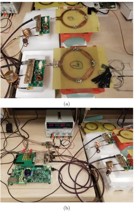
The measurement setup for coupled Class-E amplifiers, placement of phantoms and control part is shown in Fig 3.2. For high power measurements, voltage supplies with higher current capability are used instead of regular ones. With lab experiments, the performance of coupled Class-E amplifiers are investigated and it is shown that they can operate with high efficiency and desired output power by optimizing the circuit parameters of Class-E amplifier.
(a)
(b)
Figure 3.2: (a) Measurement setup for coupled Class-E amplifiers (b) Setup of FPGA evaluation board and amplifier control part.
3.2.2
MRI Experiment of Coupled Class-E Amplifiers
To investigate the effect of coupling, MRI experiments with 4-channel transmit coil are conducted in 1.5 T MRI Scanner (Scimedix Inc., Incheon, South Korea). The FPGA is given 63.795 MHz RF signal, and 2ms sinc pulse signal is gener-ated by the modified Class-E amplifiers. The amplifier is controlled by the LVDS signals generated in the FPGA and a CAT7 cable is used for sending these LVDS signals to the amplifier. An unblank signal is received from the MRI spectrom-eter in order to trigger the Class-E amplifier. Also, an RF signal at the center frequency of the MRI scanner (63.795 MHz) is given from the spectrometer to FPGA in order to generate gate driver signals at that frequency. To receive the MRI signal, system’s head coil or body coil for 1.5T are used depending on the structure of the coil setup. Data acquisition parameters of the MRI experiment is listed in Tab. 3.1. The details about the experimental setup are given in Section 4.3.2.
Parameter Value
Sequence Type Gradient Echo (GRE) Field of view (FOV) 500 mm
Slice Thickness 5 mm RF Pulse Length 2000 us Receive Gain 15 Receive Bandwidth 31.3 kHz Matrix Size 256 x 256 Slice Interleave 4
The unblank signal and RF signal at Larmor frequency (63.795 MHz) from the MRI Spectrometer are given to the FPGA. Then, LVDS signals controlling the amplifiers are generated in the FPGA. Voltage supply, the computer and FPGA are placed in MRI system component room. Using the penetration panel, LVDS signals are sent to the each amplifier channel by CAT7 cables. Also supply voltage is sent by the coaxial cables for each channel. As Class-E amplifier circuit, the design of the previous study is used [13]. The diagram of MRI experiment setup is shown in Fig 3.3.
Chapter 4
Results
In this section, MATLAB model outputs, simulation and measurement results are presented. Firstly, single Class-E amplifier is simulated and tuned by the state-space model in a numerical computing environment (Matlab R2016b, MathWorks, Natick, MA). Model results are compared and verified with simulation results in a circuit simulator (LTspice IV, Analog Devices, Norwood, MA). Effects of cir-cuit parameters on the amplifier characteristics (output power, drain efficiency, i.e.) are investigated. Then, results of coupled Class-E amplifier model are pre-sented. Effects of circuit parameter variations on the tuning, overall efficiency and output power are observed. Tuning of amplifier components is performed by using coupled Class-E amplifier model in MATLAB. Amplitude and phase of second amplifier is varied in order to observe effects on the characteristics of coupled amplifiers. Next, hardware experiments of Class-E power amplifier are done, power and efficiency measurement results are presented. Finally, MRI ex-periment is performed with Class-E amplifiers to figure out effect of coupling and related MRI images are shown.
4.1
Single Class-E amplifier Results
4.1.1
State-Space Model
Circuit parameters are calculated theoretically for 64MHz operating frequency and entered into the state-space model of single Class-E amplifier. Using the steady-state matrix analysis method, the waveforms of single Class-E amplifier are generated in the numerical computing environment. Circuit parameters are listed below:
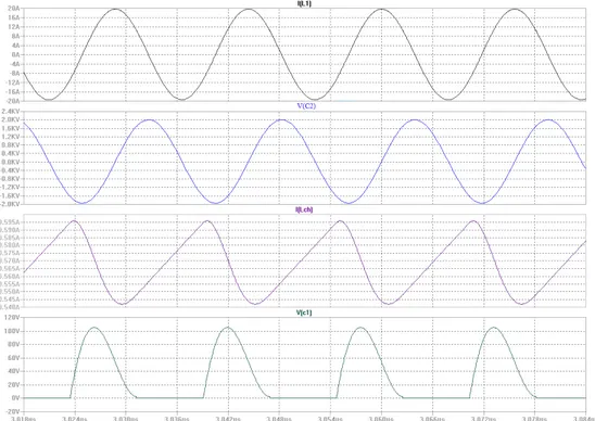
R=1.6, L1=256 nH ,Lchoke=5 uH, Vdd=30 V, C1=290 pF, C2=24.6 pF,
pe-riod=15.625 nsec
Figure 4.1: Class-E amplifier steady state waveforms for load current IL1, series
capacitor voltage VC2, the choke inductor current ILch and the switch voltage VC1
Drain efficiency and the output RF power of the Class-E amplifier is calculated as 99% and 322 W respectively.
4.1.2
Circuit Simulation
Using the same parameters, Class-E amplifier is simulated in the circuit simulator. The circuit and simulation parameters are shown in Fig. 4.2.
Figure 4.2: Circuit simulation parameters of Class-E amplifier
Results of the simulation and corresponding waveforms are shown in Fig. 4.3. In order to verify the state-space model of single Class-E amplifier, resulted data of the model and LTspice simulation of the same circuit are compared with each other in Tab. 4.1. It is observed that the results for each state variable are consistent and the error between state-space model and the simulation is not significant.
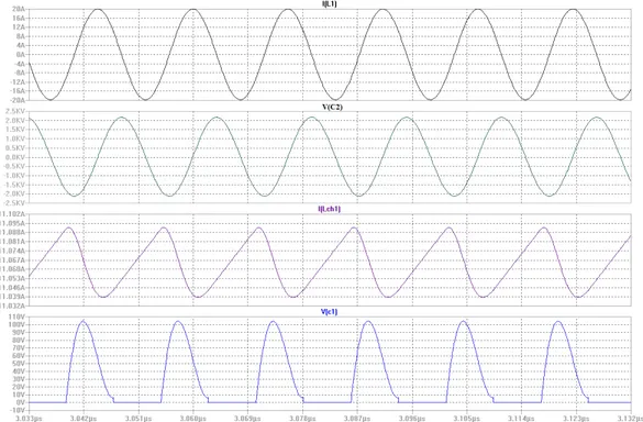
Figure 4.3: Resulted waveforms of LTspice simulation for load current IL1, series
capacitor voltage VC2, the choke inductor current ILch and the switch voltage VC1
respectively.
Parameters The State-Space Model Circuit Simulation IL1 (Peak value) 20.2 A 19.7 A VC2 (Peak value) 2050 V 2000 V ILch (Average) 10.7 A 10.6 A VC1 (Peak value) 107 V 105 V Drain Efficiency 99.9% 96.6% Output RF Power 322 W 306 W
4.1.3
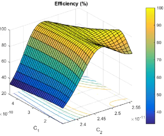
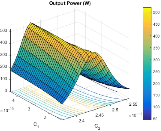
Tuning Capacitors
In order to achieve high drain efficiency for Class-E amplifier, series and parallel capacitors of the circuit should be tuned. In this part, results of tuning procedure for a single Class-E amplifier are shown. The same circuit parameters are used for the tuning part as in Section 4.1.1. For the tuning procedure, parallel capacitor C1 is swept from 120 pF to 450 pF and series capacitor C2 is swept from 23.6
pF to 25.6 pF. The amplifier characteristics are more sensitive to variation of C2 therefore the sweep range of C2 is kept small relative to the sweep range of
C1. By using the MATLAB model, tuning procedure can be performed, thus the
output power can be adjusted and capacitor values can be determined for high efficiency operation.
Figure 4.5: Output power of the amplifier with respect to C1 and C2
4.1.4
Load Variations
Operation of the Class-E amplifier is sensitive to load impedance. A variation in load impedance may cause severe degradation in drain efficiency and the output RF power. In this part, effect of component variation on the amplifier character-istics is observed. Using the state-space model, the load resistor R1 and the load
inductor L1are varied in a range. The change in the amplifier drain efficiency and
output power is calculated in the numerical computing environment and shown in Fig. 4.6 and Fig. 4.7 separately. For the load variation, the load inductance L1 is swept from 240 nH to 270 nH and the load resistance R1 is swept from 1.2
The change of R1 affects the output power of the amplifier inversely. As R1
decreases, the delivered RF power increased significantly. Also, the amplifier characteristics are very responsive to the variation of L1. A slight change in the
load inductance L1 can cause a considerable degradation in the drain efficiency
and the output power up to 15% and 20 W respectively.
4.2
Coupled Class-E amplifiers
In this part, results of coupled Class-E amplifiers are presented. Different effects such as coupling degree between the coils, phase of the amplifier and load variation are considered. The state-space model of coupled Class-E amplifiers are utilized, also simulations are performed in the circuit simulator.
4.2.1
State-Space Model
In the model, coupling degree between amplifiers can be adjusted by coupling coefficient (k). In order to generated steady state waveforms for each state vari-able, circuit parameters are determined and the coupling coefficient is adjusted to k=0.10. Coupled model parameters are listed:
R1=1.6, L1=256 nH ,Lch1=5 uH, Vdd1=30 V, C1=290 pF, C2=22.98 pF
R2=1.6, L2=256 nH ,Lch2=5 uH, Vdd2=20 V, C3=290 pF, C4=21.39 pF
Period=15.625 nsec, phase difference between switch drive signals= 0◦
Overall drain efficiency and total output RF power of the coupled Class-E amplifiers are calculated as 99% and 491 W respectively. 335 W of total RF power is delivered from the first amplifier and 156 W of total RF power is delivered from the second one. The resultant waveforms for each state variable are shown in Fig. 4.8 and Fig. 4.9. Sinusoidal currents are generated along the loads R1 and
R2. Also the switch voltage waveforms of the first channel VC1 and of the second
Figure 4.8: First channel’s steady state waveforms for load current IL1, series
capacitor voltage VC2, the choke inductor current ILch1 and the switch voltage
Figure 4.9: Second channel’s steady state waveforms for load current IL2, series
capacitor voltage VC4, the choke inductor current ILch2 and the switch voltage
4.2.2
Circuit Simulation
Using the same parameters, coupled Class-E amplifiers are simulated in LTspice. The circuit and simulation parameters are shown in Fig. 4.10.
Figure 4.10: LTspice simulation parameters of coupled Class-E amplifier Results of the simulation and corresponding waveforms for each amplifier chan-nel are shown in Fig. 4.11 and Fig. 4.12. In order to verify the state-space model of single Class-E amplifier, resulted data of the model and the simulation of the same circuit are compared with each other in Tab. 4.2. It is observed that the results for each state variable are consistent and the error between state-space model and the circuit simulation is not significant.
Parameters State-Space Model Circuit Simulation IL1 (Peak value) 20.6 A 20.0 A VC2 (Peak value) 2240 V 2170 V ILch1 (Average) 11.3 A 11.1 A VC1 (Peak value) 106 V 104 V IL2 (Peak value) 14.1 A 13.6 A VC4 (Peak value) 1640 V 1590 V ILch2 (Average) 7.6 A 7.5 A VC3 (Peak value) 72.1 V 70.7 V Drain Efficiency 99.9% 96.1% Output RF Power 491 W 462 W
Table 4.2: Comparison of the coupled amplifier model and the circuit simulation when coupling between amplifiers is 10%.
Figure 4.11: First amplifier’s simulation waveforms for load current IL1, series
capacitor voltage VC2, the choke inductor current ILch1 and the switch voltage
VC1 respectively.
These figures show that sinusoidal RF currents across R1 and R2 are
gener-ated by coupled Class-E amplifiers for a coupling level of 10%. DC currents are supplied by choke inductors Lch1 and Lch2. The switch voltage waveforms do
not satisfy ZVS and ZVDS conditions in the circuit simulator for these circuit parameters, therefore a fine tuning is required in the simulator. However, the purpose of this section is to compare results of state-space model and results of circuit simulator for the same circuit parameters.
Figure 4.12: Second amplifier’s simulation waveforms for load current IL2, series
capacitor voltage VC4, the choke inductor current ILch2 and the switch voltage
4.2.3
Effect of Coupling
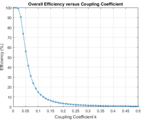
Coupling degree plays a significant role in amplifier performance. In order to show dependency of the coupled amplifier characteristics on the coupling degree between coils, a simulation is performed by utilizing coupled amplifiers MAT-LAB model. Two Class-E amplifiers are formed with the same parameters as in Section 4.1.1. Initially, there is no coupling between each amplifier channel. Then, a coupling is introduced between the load inductors and the change in the performance of the amplifiers is investigated. Results of this simulation is shown in Fig. 4.13. For extreme coupling levels, performance of the coupled system is significantly affected by the coupling degree between the amplifiers and the drain efficiency dropped below 15%, when the coupling is to 10% (k=0.10). However, if the coupling degree is limited by 3%, the overall efficiency of coupled system does not drop below 90%.
Figure 4.13: Overall drain efficiency of coupled amplifiers versus varying coupling coefficient k.
4.2.4
Tuning Capacitors
When two channels are coupled, the effective inductance of transmit coil changes, so tuning point shifts. This effect distorts the resonance frequency and reduces the efficiency of the amplifiers. In order to improve the overall efficiency in the coupled system, capacitors should be tuned. In Section 4.2.3, the effect of coupling over the system performance is demonstrated. Then, tuning of series load capacitors (C2 and C4) is performed with the same circuit parameters in Section 4.2.3. The
series load capacitor value Cs is decreased to achieve similar output power with
high drain efficiency. For each coupling level, optimum load capacitor value and corresponding output RF power are listed in Tab. 4.3. By tuning the series load capacitors (C2 and C4), ideal drain efficiency can be achieved with similar output
power performance for coupled Class-E amplifiers. For each coupling level, 99% drain efficiency is achieved with the tuned Cs values.
Coupling Coefficient Cs(pF) Output RF Power(W)
0.01 24.3 633 0.02 24.1 628 0.03 23.9 614 0.04 23.6 624 0.05 23.4 625 0.10 22.3 620 0.20 20.4 639 0.30 18.8 627 0.40 17.5 643 0.50 16.3 645
Table 4.3: Tuned new Cs values for each coupling degree and corresponding drain
efficiency and output power. Circuit parameters:
R1=1.6, L1=256 nH ,Lch1=5 uH, Vdd1=30 V, C1=290 pF
R2=1.6, L2=256 nH ,Lch2=5 uH, Vdd2=30 V, C3=290 pF
Also, tuning procedure can be applied for the coupled amplifiers with different phases. To demonstrate tuning of amplifiers with various phases, circuit parame-ters are changed and a delay of 60◦ is added to the second channel’s drive signal. The other parameters are kept same with the previous one and this analysis is done for two different coupling levels which are 1% and 10 % coupling.
4.2.4.1 Tuning for a coupling degree of 1%
To find optimum operating points for the coupled system, two series capacitors (C2 and C4) are swept through a wide range (from 18pF to 27pF). Output
char-acteristics of the coupled amplifiers are investigated in terms of drain efficiency, output power, power balance between channels and phase difference between load currents.
Circuit parameters:
R1=1.6, L1=256 nH ,Lch1=5 uH, Vdd1=30 V, C1=290 pF
R2=1.6, L2=256 nH ,Lch2=5 uH, Vdd2=30 V, C3=290 pF
Period=15.625 nsec, phase difference between switch drive signals= 60◦ Mutual coupling= 1% (k=0.01)
C2(pF) C4(pF) Overall Efficiency (%) Pload(W) P. Balance Phase(◦)
24.99 24.96 93.3 204 0.31 68 25.26 25.08 89.2 146 0.30 64 24.24 24.54 93.0 584 0.16 63 Table 4.4: Some optimum points for the load capacitors and corresponding output characteristics.
These plots show the resultant patterns of output characteristics which are overall drain efficiency, total output power, power balance between the channels and phase shift between output current respectively for the tuning procedure of series capacitors. Some optimum series capacitor values for the operation of coupled amplifiers are selected and shown in Tab 4.4. Under moderate coupling levels, high output RF power and the drain efficiency higher than almost 90% can be achieved with output currents of different phases.
Figure 4.14: Overall drain efficiency of coupled amplifiers versus varying series load capacitors when k=0.01.
Figure 4.15: Total output RF power versus varying series load capacitors when k=0.01.
Figure 4.16: Power balance between amplifier channels when k=0.01.
Figure 4.17: Phase difference(◦) between the load currents of coupled amplifiers when k=0.01.
4.2.4.2 Tuning for a coupling degree of 10%
The tuning procedure is repeated with the same circuit parameter except the coupling coefficient of 0.10. The sweep range of load capacitors C2 and C4 are
between 18pF and 27pF. According to the desired output specifications, series load capacitors can be adjusted. Some optimum capacitor values and output characteristics of the coupled system in given in Tab 4.5.
C2(pF) C4(pF) Overall Efficiency (%) Pload(W) P. Balance Phase(◦)
20.1 23.4 95.6 530 0.14 0 21.7 22.8 90.2 408 0.30 -3 Table 4.5: Some optimum points for the load capacitors and corresponding output characteristics.
It is observed that drain efficiency and total output power curves have a similar behaviour with respect to variation of C2 and C4 as shown in Fig. 4.18 and
Fig. 4.19. However, a strong correlation is not found between power balance curve and them as shown in Fig. 4.20. In some operating points where the overall efficiency is higher than 90% and output power is bigger than 500 W, the power balance can decrease up to 0.10. This means that 90% of the output power is delivered from the second channel and the first amplifier delivered only a small portion of total power. As a result, many criteria related with output characteristics should be taken into account while tuning the series capacitors, optimum capacitor values should be selected according to the desired output specifications of coupled Class-E amplifiers.
Figure 4.18: Overall drain efficiency of coupled amplifiers versus varying series load capacitors when k=0.10.
Figure 4.19: Total output RF power versus varying series load capacitors when k=0.10.
Figure 4.20: Power balance between amplifier channels when k=0.10.
Figure 4.21: Phase difference(◦) between the load currents of coupled amplifiers when k=0.10.
4.2.5
Effect of Amplitude and Phase Variation
The performance of Class-E amplifiers is affected by the load impedance. In order to determine optimum operating regions for overall efficiency and to observe the effect of amplitude and variation, sweep analysis is performed in MATLAB with 2-channel coupled Class-E amplifiers. Coupling between the amplifiers is selected as 1% and 20% for two cases. Initially, the amplifiers are tuned and adjusted to deliver about 600 W output power with 99% drain efficiency, when supply voltages are 30 V and no phase difference between driver signals. Then, phase and supply voltage of the second channel are swept from -180 to 180 degree and from 1 V to 31 V respectively. By the simulation, optimum operating regions are detected; effects of phase and amplitude of second channel on the overall performance is investigated.
4.2.5.1 Simulation for a loosely coupled system with the coupling co-efficient of 0.01
Initially, tuned amplifier is delivering 630 W RF power with an overall efficiency of 99%. Then, the phase of drive signal and the amplitude of supply for the 2nd channel are swept in the range. Output characteristics of the system are shown in Fig. 4.22 and Fig. 4.23.
Circuit parameters:
R1=1.6, L1=256 nH ,Lch1=5 uH, Vdd1=30 V, C1=290 pF, C2=24.36pF
R2=1.6, L2=256 nH ,Lch2=5 uH, Vdd2=(variable), C3=290 pF, C4=24.36pF
Period=15.625 nsec, phase difference between switch drive signals= (variable) Mutual coupling= 1% (k=0.01)
Figure 4.22: Overall drain efficiency versus supply voltage and phase of second channel.
Despite the load and amplitude variations, the coupled system can deliver RF power with an overall efficiency higher than 78%. Interestingly, amplifiers deliver maximum power when there is 180◦ phase difference between the switch drive signals.
Figure 4.23: Total output power of coupled amplifiers versus supply voltage and phase of second channel.
Figure 4.24: Power balance between the coupled amplifiers versus supply voltage and phase of second channel.
4.2.5.2 Simulation for a tightly coupled system with the coupling co-efficient of 0.20
Initially load capacitors C2 and C4 are adjusted to 20.44pF for the tuning and the
amplifiers deliver 639 W RF power with 99% overall efficiency. The other circuit parameters are the same with the previous simulation. Then, the amplitude and drive signal phase of the 2nd channel are varied in the range.
Results of the drain efficiency and the output power in Fig. 4.25 and Fig. 4.26 show that coupled amplifiers can operate with a drain efficiency of 80% or more and deliver RF power higher than 275 W, if the magnitude of phase difference is limited by 45◦ and second supply voltage (Vdd2) is higher than 20V. How-ever, the phase difference beyond this limit may cause significant degradation in drain efficiency even up to 10%. Also, the amount of output power is strongly af-fected by the variation of amplitude and phase difference beyond this limit. With controlling these two variables, efficiency and output power can be optimize for coupled Class-E amplifiers.
Figure 4.25: Overall drain efficiency versus supply voltage and phase of second channel.
Figure 4.26: Total output power of coupled amplifiers versus supply voltage and phase of second channel.
Figure 4.27: Power balance between the coupled amplifiers versus supply voltage and phase of second channel.
4.2.6
Load Variations
In this part, effect of load variations on the output characteristics of the coupled Class-E amplifiers is investigated. Using the MATLAB model, second amplifier’s load resistor R2 and the load inductor L2 are varied in a range. The change in
the overall drain efficiency and total output power is calculated in MATLAB and shown in Fig. 4.28 and Fig. 4.29 separately. Also the power balance between the amplifiers is shown in Fig. 4.30. For the part, the load inductance L2 is swept
from 230 nH to 280 nH and the load resistance R2 is swept from 1.2 ohm to 4.8
ohm.
Circuit parameters:
R1=1.6 ohm, L1=256 nH , Lch1=5 uH, Vdd1=30 V, C1=290 pF, C2=20.44pF
R2=(variable), L2=(variable) ,Lch2=5 uH, Vdd2=30 V, C3=290 pF, C4=20.44pF
Period=15.625 nsec, phase difference between switch drive signals= 0◦ Mutual coupling= 20% (k=0.20)
It is observed that overall drain efficiency is less sensitive to variation of R2,
while the value of L2 is very influential on the efficiency. The decrease of R2 leads
to a remarkable increase in total delivered RF power. The drain efficiency and total output power are very responsive to the variation of L2. Variation of the
load inductance L2 can cause a considerable degradation in the drain efficiency
and the total output power up to 20% and 50 W respectively. Also, the variation of L2 and R2 may shift the power balance towards one of the amplifier channels
Figure 4.28: Drain efficiency of the coupled system with respect to L2 and R2
4.3
Experimental Results
In order to verify the simulation results, some experiments are performed with coupled Class-E power amplifiers. Firstly, output characteristics of the amplifiers such as drain voltage waveform, efficiency and output power are observed in lab experiments. Effect of coupling on the drain waveform is observed for coupled amplifiers. Then, tuning procedure is performed by adjusting the variable capac-itors on the transmit coil. The correct drain voltage waveform for high efficiency is achieved by tuning capacitors on the coil.
MRI experiments are performed with different setups in 1.5T Scimedix scanner in order to investigate the effect of coupling on the MRI image quality. Firstly, loop coils are coupled, separate phantoms are placed on top of each transmit coil and system’s body coil is used as receiver for MRI signal. With this setup, 2 and 3 coupled Class-E amplifiers are tested by driving them at the same time. Then, a 4- channel transmit coil is made by using copper tape loops and head receive coil is placed inside this coil. A single Siemens phantom is put inside the head coil and each Class-E amplifier is connected to the corresponding loop coil. The amplifier channels are driven in a changing order and acquired MRI images for each case are presented.
4.3.1
Hardware Experiments
The experiments are performed with 2 Class-E amplifiers and transmit loop coils which shown in the section 3.2.1. In order to measure the current on the transmit coil and to calculate the output parameters such as drain efficiency, small pick-up coils which are matched to 50Ω at 64 MHz frequency are placed close enough to the transmit coils. Tuning of the circuit is inspected by measuring the drain voltage whether the drain waveform is satisfying zero-voltage switching(ZVS) and zero-voltage derivative switching(ZVDS) conditions or not.
A single Class-E amplifier is tuned and the drain voltage waveform is measured by an active probe N2796A (Agilent) as shown in Fig. 4.31a. Then, a second channel is placed close to the first amplifier with a distance of 8 cm. The drain waveform of the first amplifier is shown in Fig. 4.31b, while two channels are operating simultaneously. After the coupling is introduced between channels, the waveform is distorted and not satisfying ZVS and ZVDS conditions anymore. By adjusting the variable capacitors on the transmit coils, coupled Class-E amplifiers are tuned again. The measured drain voltage waveform of the first amplifier is shown in Fig. 4.31c. By optimizing the load parameters of Class- E amplifier, the coupled amplifiers can operate with high efficiency in a transmit array system.
(a)
(b)
(c)
Figure 4.31: Drain voltage waveform of the MOSFET when (a) There is no coupling between the amplifiers (b) Coupling is introduced by bringing coils closer (c) Capacitors on the coil are tuned for coupled case.
![Figure 2.5: Effect of adjusting load-network components on the voltage waveform of the switch[1]](https://thumb-eu.123doks.com/thumbv2/9libnet/5930932.123328/33.918.209.753.577.886/figure-effect-adjusting-network-components-voltage-waveform-switch.webp)