Ш
І Ш
$
f 3Ш
и
t © І й І ti Ä P i H II 1 1 ?i i f Г 8 Й Si*i^'ílrsL iA>»Ö I î » . y ¡?í ЛЛ; « Й% ·ί#4' ϊ i>. ?· <ítΗ· Ψ ^ τ
ΡΤ·) й в
^ ί'ίІ
äШ
Ά
/Г, ;.·λ ;■; ¡>. ^ t η1<\ г· ,'4·. .ϋΠί. « *i-),!' irt* 'W íí''’ii|¿ítii¡^ İt/-&>'á
i i ¿ V íifí*(¿í»ij¡ <«%'u tt » IkÍWÍ* iií'ÍfV i W δ v^.W^'oii '*
njfilr.'İÎV Ѵ.‘У^ Î'Ÿi ju>'Jít'¿¿'*¿ '«/'¿'S''» ·.♦<* . «‘'ííijiií W !».■<♦ ·ιί·ν·ΐί Jí i W Ѵй i U · * ϊ W à···
ігхщ
'·?Μ« fî>it ï * i ' W ‘v iîi'd ^ ü / ·/ Í it ■'«•if 4 ^ W >4 ·4ι(τΜ U ""‘» i ·ί ii. .V 4 'ii *Am1 ІГ»^4іЧ»<^ "w *r ii» #!'ï ?::?й ^'■■;î4T î?ÎÎ?1Γ i3î)^!;"7Îf
«k.·'-V 3u«i V' Î - ii -t ic «îh4ùÎW k >*< •ù<v«!' ’Î!t (il V. Ы
W* w* i ¡> •■A'» ^· t·' * «» Ίti a ! ' v·'" «t ■í ü'if» « 4 ЖЙ >:tv^ « > »
'Г·' ^ r й^■ ^ Г ■u'< w' k ¿ ¿ .‘ш í V / Λ ψ -'І Λ 4 i t J
« ^>-ii·;; « wi-i* ··' ν-,'Λ’ί·:;' . ,? :;^ >f< ; .■¡i)»•Mí» Mié ·*«Ι *· V· "»W Wf W >«
JH ·' ' · 4'J ώ'ύ*' *' ·4*^·';,'·■'? л '¡ χ ^ '4 j-'v, -íS -if'i, ■ ■ 'i·*^····' 'Ί ·.'*'* :■; ή « í.' '··■.., '^í"^ = ·· ■·■**■ *i.¿i ÿ. V|I> <14^ .t Ik' W í<Ki
« 3 ? ^
i 9 f b
M A P P IN G
AND
FP G A GLOBAL R O U TIN G
USING
M E A N FIELD A N N E A L IN G
A THESIS
SUBMITTED TO THE DEPARTMENT OF COMPUTER
ENGINEERING AND INFORMATION SCIENCE
AND THE INSTITUTE OF ENGINEERING AND SCIENCE
OF BILKENT UNIVERSITY
IN PARTIAL FULFILLMENT OF THE REQUIREMENTS
FOR THE DEGREE OF
MASTER OF SCIENCE
By
Ismail Haritaoglu
September, 1994
'Î4<
' 6 % И г- T
11
I certify that I have read this thesis and that in rny opinion it is fully adequate, in scope and in quality, as a thesis for the degree of Master of Science.
A sst. P ro i..< ^ v d et A y kanat (Advisor)
I certify that I have read this thesis and that in my opinion it is fully adequate, in scope and in quality, as gj^hesis for the degree of Master of Science.öJ;
r3=ri Assoc. Prof. Ömer Benli
X
'
I certify that I have read this thesis and that in my opinion it is fully adequate, in scope and in quality, as a thesis for the degree of Master of Science.
A ssfT Prof. Mustafa Pınar
Approved for the Institute of Engineering and Science:
Prof. Mehmet Bar Director of the Institute
ABSTRACT
MAPPING
AND
FPGA GLOBAL ROUTING
USING
MEAN FIELD ANNEALING
İsmail Haritaoğlu
M .S . in Com puter Engineering and Information Science
Advisor: A sst. Prof. Cevdet Aykanat
September, 1994
Mean Field Annealing algorithm which was proposed for solving combinatorial optimization problems combines the properties of neural networks and Simu lated Annealing. In this thesis, M FA is formulated for mapping problem in parallel processing and global routing problem in physical design automation o f Field Programmable Gate Array (F P G A s) A new Mean Field Annealing (M F A ) formulation is proposed for the mapping problem for mesh-connected and hypercube architectures. The proposed M FA heuristic exploits the conven tional routing scheme used in mesh and hypercube interconnection topologies to introduce an efficient encoding scheme. An efficient implementation scheme which decreases the complexity of the proposed algorithm by asymptotical fac tors is also developed. Experimental results also show that the proposed M FA heuristic approaches the speed performance of the fast Kernighan-Lin heuris tic while approaching the solution quality of the powerful simulated annealing heuristic. Also, we propose an order-independent global routing algorithm for S R A M type F P G A s based on Mean Field Annealing. The performance of the proposed global routing algorithm is evaluated in comparison with LocusRoute global router on
ACM/SIGDA Design Automation
benchmarks. Experimen tal results indicate that the proposed M FA heuristic performs better than the LocusRoute.IV
Keywords:
Mapping, Global Routing, Field Programmable Gate Arrays, Mean Field AnnealingÖZET
O R T A A L A N T A V L A M A M E T O D U K U L L A N IL A R A K
E ŞLEM E V E F P G A T E R D E K İ K A B A R O T A L A M A
P R O B L E M L E R İN İN Ç Ö Z Ü M Ü
İsmail Haritaoğiu
Bilgisayar ve Enformatik Mühendisliği, Yüksek Lisans
Danışman; Yrd. Doç. Dr. Cevdet Aykanat
Eylül, 1994
Birleşimsel eniyileme problemlerini çözmek için önerilen Ortak Alan Tavlama (M ean Field Annealing) algoritması, sinir ağları ve benzetimsel tavlama (Sim ulated Annealing) yöntemlerinin özelliklerini taşır. Bu çalışmada. Ortak A lan Tavlama algoritması Alan Programlamalı Kapı Devrelerinin (Field Pro grammable Gate Arrays) kaba rotalama problemine (Global Routing) ve par alel programlamadaki eşleme (Mapping) problemlerine uyarlanmıştır. Tezin ilk bölümünde Ortak Alan Tavlama algoritması Alan Programlamalı Kapı Devrelerinin (Field Programmable Gate Arrays) kaba rotalama problemi- ninin çözümünde kullanılmıştır. Önerilen algoritmalarının başarımları Locus- Route kaba rotalama algoritması ile kıyaslanarak değerlendirilmiştir. Deneyler algoritmaları karşılaştırmak için kullanılan standart devreler (Benchmarks) üzerinde yapılmıştır. Elde edilen sonuçlar Ortak Alan Tavlama algoritmasının kaba rotalama problemini çözmek için iyi bir alternatif algoritma olarak kul lanılabileceğini göstermektedir. Tezin ikinci bölümünde Mesh ve Hiperküp tipindeki paralel bilgisayarlarındaki eşleme problemi için daha önce önerilen algoritmalardan daha hızlı olan bir algoritma geliştirilmiş ve bu önerilen algorit manın başarımları Kernighan-Lin, Simulated Annealing ve daha önce önerilen ortak alan tavlama metotları ile kıyaslanarak değerlendirilmiştir.
Anahtar Sözcükler:
Orta Alan tavlama algoritması, Eşleme problemi. Kaba rotalama algoritmaları. Alan programlamlı kapı devreleriACKNOWLEDGEMENTS
I would like to express my deep gratitude to my supervisor Dr. Cevdet Aykanat for his guidance, suggestions, and invaluable encouragement throughout the development of this thesis. I would like to thank Dr. Ömer Benli for reading and commenting on the thesis. I would also like to thank Dr. Mustafa Pınar for reading and commenting on the thesis. I owe special thanks to Dr. M ehm et Baray for providing a pleasant environment for study. I am grateful to m y family and m y friends for their infinite moral support and help.
Bu çalışmamı,
herşeyimi borçlu olduğum
anneme, babama,
ve
Esine
adıyorum.
Contents
1 INTROD UCTION
1
2 M EAN FIELD AN N EALIN G
4
2.1 Mean Field Annealing ... 4
2.1.1 Ising M o d e l ... 5
2.1.2 Potts M o d e l ... 6
2.1.3 M FA A lg o r ith m ... 8
3 FPGAs & GLOBAL ROUTING
9
3.1 Introduction to Field Programmable Gate A r r a y s ... 93.1.1 Logic B lo c k s ... 10
3.1.2 Programming Technologies... 10
3.1.3 Routing A r c h it e c t u r e s ... 11
3.2 Physical Design Automation of F P G A s ... 15
3.2.1 P a r titio n in g ... 15
3.2.2 Placement 15 3.2.3 R o u t i n g ... 15
3.3 Global Routing Problem in Design Autom ation of F P G A s . . . 16
3.4 Model of F P G A for Global R o u t in g ... 17
4 MFA SOLUTION FOR GLOBAL RO UTIN G IN FPGA
22
4.1 M F A Formulation of Global R o u t i n g ... 22 4.2 Im p lem e n ta tio n ... 25 4.3 Experimental R e s u lt s ... 27
5 TH E M APPIN G PROBLEM
33
5.1 The Mapping P r o b l e m ... 33 5.2 The Model of Mapping P r o b le m ... 35
6 MFA SOLUTION FOR M APPIN G
39
6.1 General M FA Formulation for Mapping P r o b le m ... 39 6.2 Interconnection-Topology Specific M F A Formulation for Mapping 42
6.2.1 M FA formulation for Mesh-Connected Architectures . . . 42 6.2.2 M FA Formulation For Hypercube Architecture ... 51 6.3 Performance Evaluation ... 56 6.4 Experimental R e s u lt s ... 59
7 CONCLUSION
69
List of Figures
2.1 Mean Field Annealing A l g o r i t h m ... 8
3.1 The Architecture of General F P G A ... 11 3.2 Example of flexibilities of F P G A (a) flexibility of switch block
(b) flexibility of connection b lo c k ... 12 3.3 The Architecture of Xilinx 3000 F P G A ... 13 3.4 The Architecture of Actel F P G A ... 14 3.5 General approach to F P G A routing a) Global routing b) De
tailed r o u t i n g ... 16 3.6 Sample two bends r o u t e s ... 17 3.7 The F P G A model used for Global R o u t in g ... 18 3.8 (a) The routing area of the two-pin net and its subnets, (b) The
possible routes for each s u b n e t s ... 19 3.9 The Cost Graph for F P G A m o d e l ... 20
4.1 Channel density distribution obtained by M F A for the circuit
C1355
... 32 4.2 Channel density distribution obtained by LocusRoute for thecircuit
Cl355
... 32 4.3 S E G A detailed router results of the circuitC l355
for the globalrouting solutions obtained by (a) M FA (b) L o c u s R o u t e ... 32
LIST OF FIGURES
5.1 An exam ple of mapping problem 38
6.1 The proposed efficient M FA algorithm for the mapping problem
for mesh-connected Architectures. 48
6.2 Three different ways for dividing 3-dimensional hypercube to 2 2-dimensional s u b c u b e s... ... 52 6.3 The Mean field value calculation of given spin i of subcube . 56
List of Tables
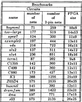
4.1 M C N C benchmark circuits used in e x p e r im e n t s ... 27 4.2 The Global Router r e s u l t s ... 28 4.3 The S E G A detailed routing results in area optimization mode . 29 4.4 The S E G A detailed routing results in speed optimization mode . 30 4,5' Minimxm Channei W idth for 100% r o u t i n g ... 31
6.1 Total communication costs averages normalized with respect to mesh-specific M F A o f the solution found by SA,KL,general M FA and mesh-specific M F A for randomly generated mapping prob lem instances for various mesh s i z e ... 59 6.2 Percent computational load imbalance averages of the solution
found by SA,KL,general M FA and mesh-specific M F A for ran domly generated mapping problem instances for various mesh s i z e ... 60 6.3 Execution time averages of the solution found by SA,KL,general
M FA and mesh-specific M FA for randomly generated mapping problem instances for various mesh s i z e ... 60 6.4 Average performance measures of the solution found by SA , KL,
general M FA and mesh-specific M FA for randomly generated mapping problem instances... 61 6.5 The Benchmark Sparce Matrix data used in experiments . . . . 62
LIST OF TAFiLES
Xll
6.6 Total communatication cost averages, normalized with respect to mesh-specific M F A , of the solution found by S A ,K L , general M FA and mesh-specific M FA for some bechmark mapping prob lem instances for various mesh s i z e ... 63 6.7 Load Imbalanced averages,of the solution found by S A ,K L , gen
eral M FA and mesh-specific M FA for some bechmark mapping problem instances for various mesh s i z e ... 64 6.8 Total execution tim e, normalized with respect to mesh-specific
M F A , of the solution found by .SA,KL, general MFA and mesh- specific M F A for some bechmark mapping problem instances for various mesh s i z e ... 65 6.9 Average performance measures of the solutions found by S A ,
K L, general M F A and mesh-specific M FA for mapping problem instances... 66 6.10 Total communication costs averages normalized with respect to
hypercube-specific M F A of the solution found by SA,KL,general M FA and hypercube-specific M FA for randomly generated m ap ping problem instances for various hypercube s i z e ... 66 6.11 Percent computational load imbalance averages of the solution
found by SA,KL,general M FA and hypecube-specific M F A for randomly generated mapping problem instances for various hy
percube s i z e ... 67 6.12 Execution tim e averages of the solution found by SA,KL,general
M F A and hypercube-specific M FA for randomly generated m ap
Chapter 1
IN T R O D U C T IO N
A common property of both domain mapping problem in parallel processing and global routing in V LSI is that both problems are combinatorial optim iza tion problems. As many problems in VLSI, parallel processing and other areas, these algorithms involve a finite set of configuration from solutions satisfying a number of rigid requirement are selected. The objective of combinatorial optimization algorithm is to find a solution of the optimum cost provided that a cost can be assigned to each solution. Many combinatorial optimizations problems are hard in the sense that they are NP-hard problems. There are no known deterministic polynomial time algorithms to find the optimal solution to any of those hard problems. The algorithms using the complete enumeration techniques are usually exponential in the size of problem, therefore they require a great amount of time to find the optimal solution. As a result, heuristics that run in a low order polynomial time have been employed to obtain good solu tions to these hard problems. Disadvantage of heuristics is that they may get stuck in local minima.
A powerful method for solving combinatorial optimization problem used in previous research is called
Simulated Annealing.
This method is the applica tion of a successful statistical method, which is used to estimate the results of annealing process in statistical mechanics, to combinatorial optimization prob lems. Simulated Annealing is a general method that guarantees to find the optimal solution if time is not limited. But time needed for Simulated Anneal ing is too much and exact solution of NP-hard problems are still intractable. Properties of Simulated Annealing are that, it can be used as a heuristic to ob tain near optimal solutions in limited time, and as the time limit is increased.CHAPTER 1. INTRODUCTION
quality of the obtained solutions also increase. An important property of Sim ulated Annealing is the ability to escape from local minima if sufficient time is given. Simulated Annealing has been applied to various NP-hard optimization problem and for most problem it gives good results.
The subjects of this thesis is a recent algorithm, called Mean Field A n nealing (M F A ) was originally proposed for solving the traveling salesperson problem. M FA is general strategy and can be applied to various problem with suitable formulations. Work on M FA showed that, it can be successfully ap plied to combinatorial optimization problems. Mean Field Annealing (M F A ) merges collective computation and annealing properties of Hopfield Neural Net works (H N N ) and Simulated Annealing (S A ), respectively, to obtain a general algorithm for solving combinatorial optimization problems. M F A can be used for solving a combinatorial optimization problem by choosing a representation scheme in which the final states of the
spins
can be decoded as a solution to the target problem. Then, an energy function is constructed whose global minimum value corresponds to thebest solution
of the problem to be solved. M F A is expected to compute thebest solution
to the target problem, starting from a randomly chosen initial state, by minimizing this energy function. In this thesis, M FA is formulated for the mapping problem in parallel processing and global routing problem in design automation of Field Programmable Gate Arrays.The first combinatorial optimization problem, that is solved by M FA in this thesis, is global routing problem in design automation of field programmable gate arrays. This study investigates the routing problem in Static R A M Field Programmable Gate Arrays (F P G A ’s) implementing the non-segmented (X il- inx based) network [27]. As the routing in F P G A ’s is a very complex combina torial optimization problem, routing process can be carried out in two phases ;
global routing
followed bydetailed routing
[11]. Global routing determines the course of wires through sequences of channel segments. Detail routing determines the wire segment allocation for the channel segment routes found in the first phase which enable feasible switch box interconnection configura tions [2-5, 14]. Global routing in F P G A can be done by using global routing algorithm proposed for standard cells [25].LocusRoute
global router is one of this type of router used for global routing in F P G A ’s [24] which divides the multi pin net’s into two-pin net’s and considers only minimum distance routes for these two-pin nets. The objective in the LocusRoute is to distribute the connections among channels so that channel densities are balanced. In thisCHAPTER 1. INTRODUCTION
thesis, we propose a new approach the solution of global routing problem in F P G A ’s by using Mean Field Annealing technique.
Second problem that is solved by M FA is the
Mapping
problem [4, 8, 29]. The mapping problem arises as parallel programs are developed for distributed memory architectures. Various classes of problems can be decomposed into a set of interacting sequential subproblems (tasks) which can be executed in par allel. In these classes of problems, the interaction patterns among the tasks is static. In a distributed-memory architecture, a pair of processors communicate with each other over a shortest path of links connecting them. Hence, commu nication between each pair of processors can be associated with relative unit communication cost. Unit communication cost between a pair of processors can be assumed to be linearly proportional to the shortest path distance between those two processors. The objective in mapping subproblems to processors of multicomputers is the minimization of the expected execution time of the par allel program on the target architecture. Thus, the mapping problem can be modeled as an optimization problem by associating the following quality mea sures with a good mapping : (z) interprocessor communication overhead should be minimized,(ii)
computational load should be uniformly distributed among processors in order to minimize processor idle time. The mapping problem has been solved by using Simulated Annealing, Kernighan-Lin type heuristic before. Also the M FA has been formulated in [6, 5]. But this formulation was a general formulation for any type of multicomputer whose intercommunication topologies are known. In this thesis we propose an efficient M FA formulation for topology-specific mapping for 2D-m esh and hypercube. For each intercon nection topology, the efficient M F A formulation is given instead of using one general formulation as in [6].In Chapter 2 the theory of the Mean Field Annealing heuristic and its en coding models are explained. The Field Programming Gate arrays, its design automation and Global Routing problem are introduced in Chapter 3. Also the F P G A model for global routing problem are proposed in this chapter. Chap ter 4 gives the M FA formulation of global routing problem in F P G A s design automation. The mapping problem are introduced in Chapter 5. Chapter 6 presents general M FA formulation the topology-specific M FA formulation for Domain Mapping problem. Finally, conclusion of thesis are stated in Chapter?.
Chapter 2
M E A N FIELD A N N E A L IN G
In this chapter the Mean Field Annealing (M F A ) heuristic is introduced and its models are given.
2.1
Mean Field Annealing
Mean Field Annealing (M F A ) merges collective computation and annealing properties of Hopfield Neural Networks (H N N ) and Simulated Annealing (S A ), respectively, to obtain a general algorithm for solving combinatorial optim iza tion problems. H N N is used for solving various optimization problems and reasonable results are obtained for small size problems. However, simulations of this network reveals the fact that it is hard to obtain
feasible solutions
for large problem sizes. Hence, the algorithm does not have a good scaling prop erty, which is a very important performance criterion for heuristic optimization algorithms. M F A is proposedas
a successful alternative to H N N . In the M FA algorithm, problem representation is identical to H N N , but iterative scheme used to relax the system is different. M FA can be used for solving a combi natorial optimization problem by choosing a representation scheme in which the final states of thespins
can be decoded as a solution to the target prob lem. Then, an energy function is constructed whose global minimum value corresponds to thebest solution
of the problem to be solved. M FA is expected to compute thebest solution
to the target problem, starting from a randomly chosen initial state, by minimizing this energy function. Steps of formulating M F A technique for a combinatorial optimization problem can be summarized as follows :CHAPTER 2. MEAN FIELD ANNEALING
• Choose a representation scheme which encodes the configuration space of the target problem using spins. In order to get a good performance, number of possible configurations in the problem domain and the spin domain must be equal, i.e., there must be a one-to-one mapping between the configurations of spins and the problem.
• Formulate the cost function of the problem in terms of spins, i.e., de rive the energy function of the system. Global minimum of the energy function should correspond to the global minimum of the cost function. • Derive the mean field theory equations using this energy function, i.e.,
derive equations for updating expected values of spins.
• Minimize the complexity of update operations in order to get an efficient algorithm.
• Select the energy function and the cooling schedule parameters.
The M F A algorithm is derived by analogy to
Ising
andPotts model
which are used to estimate the state of a system of particles, called spins, in thermal equilibrium.2.1.1
Ising Model
In Ising model spins can be in one of two states represented by 0 and 1. In the Ising model, the energy of a system with
S
spins has the following form:1
(
2
.
1
)
k=l1фк
fc=lHere, indicates the level of interaction between spins
к
and /, andSk
€ { 0 ,1 } is the value of spink.
It is assumed that¡3ki
=Pik
and = 0 forI < k,l,< S.
At thermal equilibrium, spin average (sjt) of spin
к
can be calculated using Boltzmann distribution as follows1
-f
e-'t'k/T
(2.2)
Here,
<f>k = {H{s))\s^=Q — {H{s))\s^=i
represents themean field
effecting on spinCHAPTER 2. МЕЛА' FIELD ANNEALING
( / / ( s ) ) — ^
Y20ki{skSi)
+ ^hk{sk)
h=l Ijtk
k=l
(2.3)
The complexity of computing
4>k
using Eq.2.3 is exponential. However, for large number of spins,mean field approximation
can be used to compute the energy average as(^(s)> = i E
E M M +
E
M
(
2
.
4
)
“ k = l l^k k = l
Since
{H{s))
is linear in(sk),
mean field<f>k
can be computed using the following equation.h
= (/i(s)>l,.=o - {//(s))i„=. =
= -
\ E M
+
(
2
.
5
)
2.1.2
Potts Model
In the Potts model, spins can be in one of the
K
states. In state Potts model ofS
spins, the states of spins are represented usingS
/f-dim ensional vectors Sj = [5,1, . . . ,Sik
, . . . , 1 < i < -S, where “i” denotes the vector transpose operation.The spin vector Si is allowed to be equal to one of the principal unit vectors e i , · . · , ©k) · · ·) ®K) and can not take any other value. Principal unit vector is defined to be a vector which has all its components equal to 0 except its ¿ ’th component which is equal to 1. Spin Si is said to be in state
k
if it is equal to efc. Hence, aK
state Potts spin Si is composed of two state variablesSii,... ,Sik,... 1
SiKi
where s,·* € { 0 , 1 } , with the following constraintк
Y^Sik = G
^ < i < S
k=l
(
2
.
6
)
In the Potts model, the energy of a system with
S
K-state Potts spin has the following form:^ = i E E f t - s , s , + E ' A
i= l
j:^i
i=l
(2.7)
Here,
fiij
indicate the level of interaction between spinsi
andj,
and interaction between Potts spins S ,S j is formulated as^ikSji·
Therefore weCHAPTER 2. MEAN FIELD ANNEALING
can formulate the energy of the system as
s
к к
^
t = lk=ll=l
(
2
.
8
)
1=1 1=1
Here,
Sik
e 0,1 is the value of A:th state of the Potts spini.
At thermal equilibrium, spin average (s,jt) of spinг
can be calculated using Boltzmann distribution as follows{Sik) =
оФ.к/Т
(2.9) Here,
(sik)
€ [0,1]. Note thatSik
can be 0 or 1 but (s,jfc) can be any real value between 0 and 1. represents themean field
effecting on statek
of spini.
The mean field value for Potts spin
i
can be formulated asfe = {i^(s))ls,=o-{//(s))|s.=
. M Md{sik)
Z
Z
b¥»· i=i (2
.10
)(
2
.
11
)
A t each temperature, starting with initial spin averages, the mean field effecting on a randomly selected spin is found using Eqs. (2.5) and (2.10). Then, spin average is updated using Eq. (2.2) and Eq. (2.9) This process is repeated for a random sequence of spins until the system is stabilized for the current temperature. M F A algorithm tries to find equilibrium point of a system of
S
spins using annealing process similar to SA,. The state equations used in M FA are isomorphic to the state equations of the neurons in the H N N . A synchronous version of M F A , can be derived by solvingN
difference equations forN
spin values simultaneously. This technique is identical to the simulations of H N N done using numerical methods. Thus, evolution of a solution in a H N N is equivalent to the relaxation toward an equilibrium state affected by the M F A algorithm at a fixed temperature [9]. Hence M FA can be viewed as an annealed neural network derived from H N N . H N N and SA methods have a major difference: SA is an algorithm implemented in software, whereas H N N is derived with a possible hardware implementation in mind. M FA is somewhere in between, it is an algorithm implemented in software, having potential for hardware realization [8, 9]. In this work, M FA is treated as a software algorithm as S A . Results obtained are comparable to other software algorithms, conforming this point of view.CHAPTER 2. MEAN FIELD ANNEALING
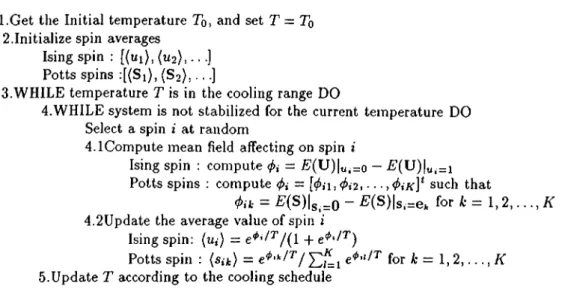
l.G et the Initial temperature Tq, and set T = Tq
2.Initialize spin averages
king spin : [(ui), («
2
), . . . ]Potts spins :[(Si), (
82
), · · ·]3.WHILE temperature T is in the cooling range DO
4. WHILE system is not stabilized for the current temperature DO
Select a spin i at random
4 .¡Compute mean field affecting on spin i
Ising spin : compute (f>i - E'(U)|t,,=o
-Potts spins : compute <t>i = [<t>i\,<i>i2, · · ·, <t>iKY such that
= ^ ( S ) |s
,^0
- ^(S)|s.= e* for i = 1 , 2 , . . AT4.2Update the average value of spin i
Ising spin: {ui) = -f
Potts spin : {sik) = ioT k = 1, 2, . . . , K
5. Update T according to the cooling schedule
Figure 2.1. Mean Field Annealing Algorithm
2.1.3
MFA Algorithm
The Mean Field Annealing algorithm are summarized in Figure 2.1.2. Begin ning of the algorithm, the initial temperature are initialized and the current temperature is set to that initial value (step 1). After that Ising and Potts spins are initialized (step 2). Then, the annealing property of M F A are begin. In cooling schedule, the system tries to reach a stable state for each tempera ture until most of spins converges a stable state. For each temperature, while the system is not in stable state, a spin is selected randomly (step 4 .1 ), and mean field values of spins are calculated (step 4.2) in order to update the spin values (step 4.3). When the system reaches the stable state, the temperature decreased by cooling schedule (step 5). At the end of algorithm, when most of spins converge, spins are decoded for a solution of target problem.
Chapter 3
F P G A s & GLOBAL R O U T IN G
This chapter introduces the Field Programmable Gate Arrays and its physical design automation steps briefly. Routing architectures of F P G A ’s are men tioned in this chapter and global routing problem and its previous solutions are given at the end of this chapter. Also the global routing problem in F P G A s is modeled in this chapter.
3.1
Introduction to Field Programmable Gate Arrays
Field Programmable gate arrays (F P G A s) are new electrically programmable integrated circuits that provide high integration and rapid turnaround time. In V L SI design automation, the fabrication tirne is important problem. In order to reduce time to fabricate interconnects, programmable devices have been introduced. F P G A is very popular programmable devices used in A SIC design market.
F P G A can reduce manufacturing turnaround time and cost. In its simplest form, an F P G A consists of an array of programmable logic blocks and routing network to interconnect the logic blocks. The programmable logic blocks can be programmed by the user to implement a small logic function. An important property of F P G A is re-programmability by using electrically programmable switches. Commercial F P G A ’s differ in the type of programming technology used, in architecture of logic blocks and their routing architectures. An F P G A logic blocks can be as simple as transistor or as complex as a microprocessor.
CHAPTER 3. FPGAS S¿ GLOBAL ROUTING
10
It is typically capable of implementing many different combinational and se quential logic functions. F P G A ’s logic blocks can be classified as transistors pairs, basic small gates (such as two-input N A N D ’s), multiplexes and Look-up tables.
3.1.1
Logic Blocks
F P G A s logic blocks differ greatly in their size and implementation capability. The two transistor logic block can only implement an inverter but is very small in size, while look-up table logic blocks used in Xilinx F P G A s can implement any five-input logic function but they are significantly larger. Logic blocks can be classified in terms of granularity. Granularity can be defined in various ways, for example, as the number of boolean function that the logic block can implement, the number of equivalent two input N A N D gates, total number of transistors, number of inputs and outputs. But generally, the commercial logic blocks can be classified into two categories:
fine-grain
andcoarse-grain.
Main advantage of using fine grain logic blocks is that the use-able blocks are fully utilized. However the main disadvantage of fine-grain blocks is that they require a relatively large number of wire segments and programmable switches.
3.1.2
Programming Technologies
An F P G A is programmed using electrically programmable switches. Accord ing the properties of these programmable switches such as, on-resistance and capacitance, programming technologies can be classified into three main types. These three types are S R A M , antifuse and E P R O M programming technolo gies.
The S R A M programming technologies uses static R A M cells to control the gates and multiplexes. In S R A M , the switch is a pass transistor controlled by the state of a S R A M bit. Therefore, S R A M is volatile. Hence The F P G A must be loaded and configured at the time of chip power-up, it requires external per manent memory to provide the programming bits such as P R O M or E P R O M . A major disadvantage of S R A M programming technology is its large area ( its takes at least five transistors to implement an S R A M cell). However, S R A M programming technology has fast re-programmability as an advantage of it.
CHAPTER 3. FPGAS ¿z GLOBAL ROUTING
11
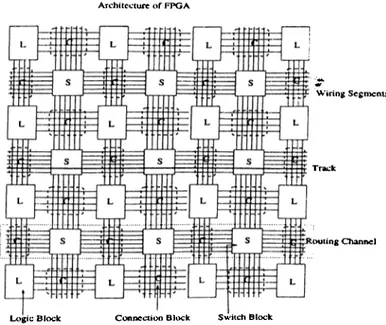
Architecture o f FPGA
Wiring Scgnicnts
outing Channel
Logic Block Connection Block Switch Block
Figure 3.1. The Architecture of General F P G A
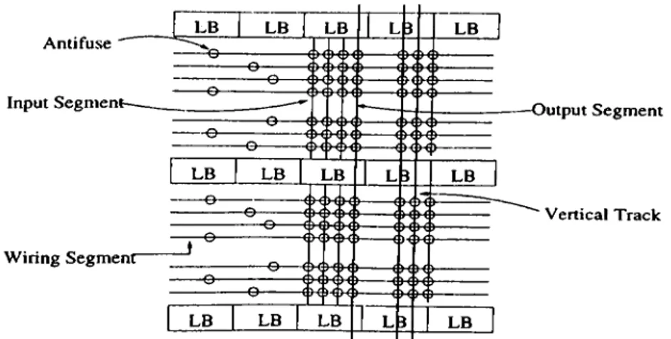
An antifuse is a two terminal device with an unprogrammed state presenting a very high resistance between its terminals. W hen a high voltage is applied across its terminals, the antifuse will blow and create low resistance link. This link is permanent. Programming an antifuse requires extra circuitry to deliver the high programming voltage and a high current. A major advantage of the antifuse is its small size.. This advantage is reduced by the large size of the necessar_v programming transistors·.
The floating gate programming technology uses technology found in ultra violet erasable E P R O M and electrically erasable E E P R O M . M ajor advantage of E P R O M technology' is its fast reprograramability. Also it does not require extra permanent memory to program the chip on power-up. However this tech nology increase the number of processing steps and high resistance transistors.
3.1.3
Routing Architectures
The routing architecture of an F P G A is the manner in which the programmable switches and wiring segments are positioned to allow the programming inter connection of the logic. Figure 3.1 illustrates a typical routing architecture model. Before giving some commercial F P G A routing architecture, giving some definition is helpful for understand routing problem in F P G A . A
wire
CHAPTER 3. FPGAS & GLOBAL ROUTISG
12
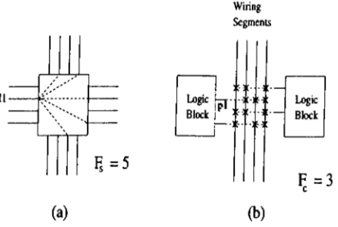
Wiring Segments Logic U · Block : Fs=5---
BlockLogic Fc=3(a)
(b)Figure 3.2. Exam ple o f flexibilities of F P G A (a) flexibility of switch block (b) flexibility of connection block
segment
is a wire unbroken by programmable switches. One or more switches may attach to the wire segment. Each end of wire segment has a switch at tached.A
track
is sequence of one or more wire segments in a line. Arouting channel
is group of parallel tracks as in Figure 3.1.As shown in Figure 3.1, the model contains two basic structures: Connec tion blocks and switch blocks. A connection block provides connectivity from the input and output of logic blocks to the wire segments in the channels. A switch block provides connectivity between the horizontal as well as the vertical wire segments.
As in Figure 3.2, The general routing structure of F P G A has two impor tant interconnection block. These are connection blocks which are used to make connections between logic block pin and routing segments, and switch blocks where connections are switched at the intersection of horizontal and vertical channels. The number of switching in connection and switch blocks is impor tant for good routability. Large number of switching increase the routability but it causes poor performance and large delay and also large area.
The number and distribution of switches used in interconnection called
flexibility
of an F P G A . Flexibility of switch blocks (F ,) and flexibility of con nection block{Fc)
can be defined as the number of choices offered to each wire enter a switching block or a connection block, respectively. Theflexibility of
switch block F,
is defined to be total number of possible connection offeredCHAPTER 3. FPGASL· GLOBAL ROETISG
13
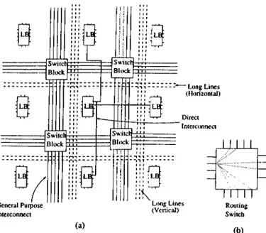
LB: Sw iictq Block LB; Swiicl· Block LB; General Purpose Interconnect L B :9
Switch BkKki SwitcH Blexrke
~ Long Lines (Horizontal) Direct Interconnect : LB:I I
Long Lines (Vcnical) (a) Routing Switch ( b ) Figure 3.3. The Architecture of Xilinx 3000 F P G Ato each wire segment. The
flexibility of connection block Fc
is defined as the number of wires that each logical pin of logic block can connect. Next section describes the important routing architecture of commercial F P G A ’s such as X ilinx and Actel.The Xilinx Routing Architecture
Figure 3.3 illustrates the routing architecture used in the Xilinx 3000 series F P G A . Connections are made from the logic block into the channel through a connection block. Since each connection site is targe because of the S R A M programming technology, the Xilinx 3000 connection blocks connects each pin to only two or three out of five tracks passing by a block . On all four sides of the logic block there are connection blocks that connect a total of 11 dif ferent logic block pins to the wire segments. Once the logic pin is connected via the connections block makes connections between segments in intersecting horizontal and vertical channels. Each wire segment can connect to five or six out of a possible 15 wire segments on the opposites sides. There are four types of wire segments provided in the Xilinx 3000 architecture:
-General-purpose interconnect consisting of wire segments that pass through switches in the switch block.
CHAPTER 3. FPGAS
&
GLOBAL ROUTING
14
Antifuse ^ Input Segment-Wiring Segment“ LB LB LB L3 LB i H C ^ i: 7^ ' 1 t } · < H H)---____ .
k. r i f f TX\ \fH H \ / )---_______ 0 _-)---_______)---________ _1.) \f \ fc r r rX7~\\ ftX\ f}\ ■ \f r t )---\ i>1 ( t---1 H H)---___
iV
- 0_____ _
^s J K" ^ f rX )---f H i--- Q __________^s } K' ^ r rX \ cwtX)--- i H )---} KfX E)---( p — LB LB LB L3 LB ---& -i Vi \ f \ f— .. .
Q____
^ ViS r \ fV )--- ( H )---________
Q ^ ViJ5 ( V J V >---( H )---O f H Vi tX >---( ^--- © — -4 )_( I K '--- 1 >■< 1 f N 4i)---___
CiKJ________
£\ ) (\ i*---€ M. )---_______
0____
(. \ ( \ i 1f \ i>---i H►--- - i H H )---) ---LB LB LB L3 LB -Output Segment ‘ Vertical TrackFigure 3.4. The Architecture of Actel F P G A
-Direct interconnect consisting of wire segments that connect each logic block output directly to four nearest neighbors.
-Long lines, which span the length or width of the chip, providing high-fanout uniform delay connections.
-Clock line, which is a single net that spans the entire chip and is driven by a high-drive buffer.
The Actel Routing Architecture
The Actel routing architecture has a eisymmetric architecture because there are more general purpose tracks in horizontal direction than vertical direction. The connection block of the Actel routing architecture is shown in Figure 3.4. The connectivity of A C T E L F P C A s is different in input and output pins. For input pins, each pin can connect to all of the tracks in the channel that are on the same side as the pin. The output pins extend across two channels above the logic block and two channels below it. Output pins can connect to every track in all four channels that is crosses. There is no separable switch block in the Actel architecture. Instead, the switching is distributed throughout the hori zontal channels. All vertical tracks can make a connection with every incident horizontal tracks. Each horizontal channel consists of 22 routing tracks, and each track is broken up into segments of different lengths. There are three type of vertical segments: input segments, output segments and freeways that either travel the entire height of chip, or some significant portion of it. This allows signal to travel longer vertical distance than permitted by output segments.
CHAPTER 3. FPGAS
GLOBAL ROUTING
15
3.2
Physical Design Automation of FPG As
The physical design automation of F P G A s involves mainly three steps which include partitioning, placement and routing.
3.2.1
Partitioning
Partitioning is the separation of the logic into Logic blocks. Partitioning has both a logical and physical component. T he connections within a logic blocks are constrained by the limited routing architecture and limited number of blocks outputs. However, the quality of the resulting partitioning depends on how well the placement can be done. The logical component has been investigated in the context of technology mapping in logic optimization.
3.2.2
Placement
Placement starts with logic blocks and input-output blocks in partitioned netlist and decides which corresponding blocks on the chip should contain them. The F P G A placement problem is very similar to traditional standard cell and gate array placement problems. Many of existing algorithm place ment algorithms are applicable, such as simulated annealing, force directed relaxation and min-cut.
3.2.3
Routing
After placement of all circuit, each pin of any multipoint net have to be con nected. There are several routing algorithms for different kind of F P G A ar chitectures and routing problem in F P G .A ’s is very complex as in standard cells and gate arrays designs. Because of simplicity, the routing problem can be divided into two step as in traditional routing problem: global routing and detailed routing.
Global routing in F P G A ’s can be done by using a global router for standard cell design. In general such a global router divides the multipoint nets into two terminal nets and routes them with minimum distance path. W hile doing so it
CHAPTER 3. ERG AS S¿. GLOBAL ROUTING
16
□
□
□
□
□
□
° ,
□
□
□
□
□
□
□
A
(a)
□
□
□
□
□
□
□
□
□
□
□
(b)□
□
□
Figure 3.5. General approach to F P G A routing a) Global routing b) Detailed routing
also tries to balance the density of channels. The global route d efin es________ route for each connection by assigning it a sequence of channel segments. After the paths are defined in terms of channel between two-pin connection detailed router chose specific wiring segments to implement the channel segment signed during global routing.
a coarse
as-3.3 Global Routing Problem in Design Automation of
FP G A s
A global router chooses channels for each net and leaves the task of allocating specific wiring segments and switches to detailed router. The global routing in F P G A ’s decides for each net to determine which pins are actually to be connected. The objective of global router is to minimize the sum of the channel densities of all channels. As in many studies, the routing problem in F P G A is solved by directly allocating the segments and ignore the global routing phase. There are unique global router for F P G A : PG Aroute. This global router similar the global router for standard cells and use the LocusRoute global routing algorithm.
In the LocusRoute algorithm, the following three steps are executed for each multi pin nets.
1) N et’s Division: Each multi-pin net is divided into a set of two-pin con nections using a minimum spanning tree algorithm.
CHAPTER 3. ERG AS & GLOBAL ROUTING
17
Tf S2 sr·· T2n
Figure 3.6. Sample two bends routes
2) Route Generation and Evaluation: In this steps, the possible paths be tween each pin of two-pin nets are considered and evaluate this paths in terms of cost value and chose the lowest cost value path.
The method of choosing routes is based on paths that have two or less bends. LocusRoute evaluates a subnet of all two bend routes between the two physical pins and chose the one with the lowest cost. The cost function is defined in terms of the channel densities. Each wire segments and switch blocks are represented as elements of an array which is called as cost array. Each element of cost array
Hij
contains the number of routes that pass through the wire segment of{i,j).
The cost of path(P) is calculated asCost(P) =
y: Hi,¡
(3.1)
3 ) Reconstruction: This step joins all two-pin connections back together, performs assigns unique numbers to distinct segments of some nets in each channel.
Locus routes uses the iterative technique, that after the first tim e all nets are routed, each is sequentially ripped up and rerouted. Iterations reduces the order dependency and also it improves the routing quality.
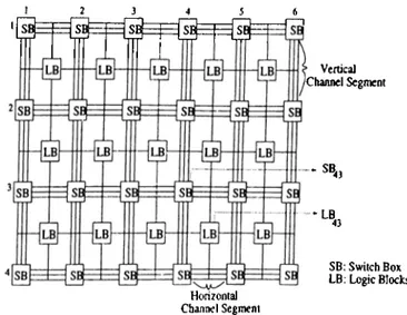
3.4 Model of F P G A for Global Routing
The form of commercial F P G A consists of a two dimensional regular array of programmable logic blocks (L B ’s), a programmable routing network and
CHAPTER 3. FPGAS &c GLOBAL ROUTING
IS
Vertical ^Channel Segment • SR, Horizontal Channel Segment LB SB: Switch Box LB: Logic BlocksFigure 3.7. The F P G A model used for Global Routing
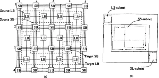
switch boxes (S B ’s) [3, 1, 2]. Logic blocks are used to provide the function ality of a circuit. Routing network makes connections between L B ’s and in- put/output pads. Routing network of F P G A consists of wiring segments and connection blocks. Wiring segments have three type of routing resources in the commercial S R A M based F P G A [Ij: channel segments, long lines and direct-interconnections. A horizontal (vertical) channel segment consists of a number of parallel wire segments connecting two successive S B ’s in a horizontal (vertical) channel. The S B ’s allow programmed interconnection between these channel segments. Direct-interconnection provides the connections between neighbor L B ’s. Long lines cross the routing area of F P G A vertically and hor izontally. Connection blocks provide the connectivity from the input/output pins of L B ’s to the wiring segments of the respective channel segments. Each pin can be connected to a limited number of wiring segments in a channel and this is called a^ flexibility of connection block [16]. In this work, it is assumed that each LB pin can be connected to all wiring segments in the respective channels. Therefore, we can omit the connection block in our F P G A model.
Since the
direct-interconnections
are used by neighbor L B ’s to provide m in imum propagation delay and thelong lines
are used by signals which must travel long distances (i.e., global clock), these interconnection resources are not considered in the global routing. Hence, our F P G A model for global rout ing considers only the L B ’s, S B ’s and channel segments. An F P G A can be modeled as a two dimensional array of L B ’s which are connected to the verti cal and horizontal channel segments, and S B ’s which make connections betweenCHAPTER 3. FPGAS & GLOBAL ROUTIXG
19
Source LB Source SB LS-subnet Target SB Target LB f ^^^-.subnet ; f ·' ; (► * I'i t : : ♦ (a) SL-subnet (b)Figure 3.8. (a) The routing area of the two-pin net and its subnets, (b) The possible routes for each subnets
the horizontal and vertical channel segments (Fig. 3.7).
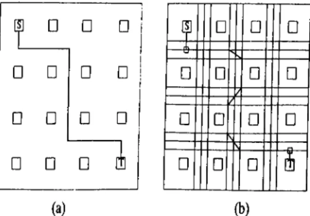
In this work, we divide all multi-pin nets into two-pin nets using minimum spanning tree algorithm [19] as in LocusRoute. Hence, a net refers to a two- pin net here, and hereafter. Consider the possible routings for a two-pin net with a Manhattan distance of
dh + dy
wheredk
and denote the horizontal and vertical distances, respectively, between the two pins of the net on the LB grid. The routing area of this net is restricted to a (d/i-t-1) x (d „-t-l) LB grid as shown in Fig. 3.8.a. Then, the shortest distance routing of this net can be decomposed into threeindependent
routings as follows. Each pin of this net has only one neighbor SB in the optimal routing area. Hence, each pin can be connected to its unique neighbor SB either through a horizontal or a vertical channel segment (Fig. 3.8). Meanwhile, the optimal routing area for the connection of these two unique S B ’s is restricted to a x d „ SB grid embedded in the LB grid (Fig. 3.8). Hence, by exploiting this fact, we further subdivide each net into three two-pin subnets referred here asLS, SS
andSL
subnets (Fig. 3.8.b). Here,LS
and 5 L subnets represent the L B -to-SB and SB -to-LB connections, respectively, andSS
subnets represent the SB-to- SB connection for a particular net. Therefore, we consider only two possible routings for bothLS
andSL
subnets anddh+dy — 2
possible one or two bend routings forSS
subnets for routing the original net.W e define an F P G A graph F (L , 5 , C ) for modeling the global routing prob lem in F P G A s. This graph is a P x Q two-dimensional mesh where
L, S
andCHAPTER 3. PPG AS
&
GLOBAL ROUTING
20
FPGA Graph
R l: A possible route for SS-subnet
R2: Two possible routes for the LS-subnet ( ) R3: Two possible routes for the SL-subnet ( S ,L ) 73 73
P’igure 3.9. The Cost Graph for F P G A model
C
denote the set of L B ’s, S B ’s and channel segments, respectively. Here,P
and
Q
is the number of horizontal and vertical channels in the F P G A . Each grid point (vertex) Sp, of the mesh represents the SB at horizontal channelp
and vertical channel
q.
Each cellLpg
of the mesh represents the LB which is adjacent to four S B ’sSpq,
■Sp.j+i, and ■Sp+i,,. Edges are labeled such that the horizontal (vertical) edge (c"^) corresponds to the channel segment between the two consecutive S B ’sSpq
and 5p,,+i (sp+i,,) on the horizontal (ver tical) channelp (q),
respectively. Figure 3.9 displays a 8 x 6 sample F P G A graph. Then, the pins of theLSISL
andSS
type subnets are assigned to the respective cell-vertex and vertex-vertex pairs of the graph as is in mentioned earlier.The global routing problem reduces to searching for most uniform possible distribution of the routes for these subnets. The uniform distribution of the routes is expected to increase the likelihood of finding a feasible routing in the following detailed routing phase. Hence, we need to define an objective function which rewards
balanced
routings. VVe associate weights with the edges of F P G A graph in order to simplify the computation of the balance quality of a given routing. The weightw^g (u>pq) of
a horizontal (vertical) edgec^g
(Cpg)
denotes the density of the respective channel segment. Here, the density of a channel segment denotes the total number of nets passing through that segment for a given routing. Using this model, we can express the balanceCHAPTI-R 3. FPGAS
&
GLOBAL ROUTISG
21
quality
B oi a.
given routing R asB ( R ) = E E « ( R ) ) " + E E K , ( R ) ) ^
P=1 q z = l q = i p = l
(3.2)
As is seen in Eq. (3.2), each channel segment contributes the square of its den sity to the objective function thus penalizing imbalanced routing distributions. Hence, the global routing problem reduces to the minimization of the objective function given in Eq. (3.2).
Chapter 4
M FA SOLUTION FOR GLOBAL
R O U TIN G IN FP G A
This chapter investigates the routing problem in Static R A M Field Pro grammable Gate Arrays (F P G A ’s) implementing the non-segmented (Xilinx based) network [27]. The architecture model of F P G A used for formulation and Mean Field Annealing formulation for global routing problem are given in this chapter. Details of experiments, the circuits used in experiments and results are shown at the end of this chapter.
4.1
M FA Formulation of Global Routing
The M FA algorithm is derived by analogy to
Ising
andPotts
models which are used to estimate the state of a system of particles, called spins, in thermal equilibrium. In Ising model, spins can be in one of the two states represented by 0 and 1, whereas in Potts model they can be in one of theK
states. AllLS/SL
subnets are represented by Ising spins since they have only two possible routes. In Ising spin encoding of eachLS/SL
subnetm,
= I
(0) denotes that the LB-to-SB or SB-to-LB routing is achieved through a single horizontal (vertical) channel segment. EachSS
subnetn
having!{„
> 2 possible routes is represented by a ATn-state Potts spin. The states of a /t"„-state Potts spin is represented using aKn
dimensional vectorVn — [^nl) · · · )