Computer-Controlled Characterization
of High-Voltage, High-Frequency SiC Devices
∗
1
J. M. Ortiz-Rodríguez, 1A. R. Hefner, Jr., 1D. Berning, 1C. Hood, 2S. Olcum
1
National Institute of Standards and Technology Semiconductor Electronics Division
100 Bureau Drive Gaithersburg, MD 20899-8120
2
Department of Electrical and Electronics Engineering Bilkent University
TR-06800 Bilkent, Ankara Turkey
Abstract∗-LA software-based high-voltage curve tracer
application for SiC device characterization is presented. This flexible application interface is developed to define testing parameters needed to control the hardware of a custom-made 25 kV-capable SiC characterization test bed. Data acquisition is
controlled for optimum resolution, and I-V characterization is
computed by means of a user-defined time interval based on the shape of the applied power pulses. Both voltage and current waveforms are displayed for each data point captured to allow the user to observe transient effects. Additionally, the software allows archiving some or all of these transient waveforms. Acquired results are shown to demonstrate functionality and flexibility of the new system.
I. INTRODUCTION
Recent breakthroughs in Silicon Carbide (SiC) material and fabrication technology have led to the development of new High-Voltage, High-Frequency (HV-HF) power devices with 10 kV, 20 kHz power switching capability [1]. The goal of the ongoing Defense Advanced Research Projects Agency (DARPA) Wide Band-gap Semiconductor Technology (WBST) High Power Electronics (HPE) program is to develop 10 kV, 100 A, 20 kHz class power semiconductor devices, therefore enabling future electric ships, more electric aircraft, and all electric combat vehicles [1, 2]. DARPA is particularly interested in developing the power electronics device technology deemed necessary to enable 2.7 MVA Solid State Power Substations (SSPS) for future Navy warships in the HPE Phase 3 program [2].
The benefits of HV-HF semiconductor technology have also been identified by the Electric Power Research Institute (EPRI), including advanced distribution automation, using solid-state distribution transformers with significant new functional capabilities and power quality enhancements. In addition, HV-HF power devices are an enabling technology for alternative energy sources and storage systems. The materialization of HV-HF devices with such capability is expected to revolutionize utility and military power distribution and conversion by extending the use of Pulse Width Modulation (PWM) technology to high voltage applications. The emergence in HV-HF power devices presents unique
∗ Contribution of the National Institute of Standards and Technology is not subject to copyright.
challenges in specifying the device requirements and establishing HV-HF PWM converter topologies. Performance metrics and measurement equipment needed to evaluate HV-HF devices and packages performance is presented in [3]. The type of measurements performed on HV-HF SiC devices can exceed the hardware limits of commercial measurement instrumentation. Therefore, custom-made systems must be developed in order to perform these demanding tests.
The performance metrics used to analyze the HV-HF devices at the National Institute of Standards and Technology* (NIST) include, among others, static, dynamic, and safe-operating-area (SOA) evaluation of SiC power diodes and switches as well as device and package reliability evaluation. The unique test equipment developed at NIST for this purpose includes: 1) a 25 kV variable pulse width curve tracer (shown in Fig. 1), 2) a 15 kV resistive and inductive load switching tester, 3) a 5 kV dI/dt and dV/dt controlled diode reverse recovery tester, 4) SiC model parameter extraction suite of tools, 5) a high-speed transient thermal current uniformity imaging system, 6) a high-speed transient thermal response system, 7) a rapid thermal cycling stress system, and 8) an automated multi-channel forward bias stress and monitoring system. Device degradation induced by forward bias stress is a reliability issue that is particularly important for minority-carrier type SiC power devices, such as PiN diodes and IGBTs [4].
Figure 1. High-voltage curve tracer circuit schematic.
The custom-made curve tracer program presented in this paper is a combination of hardware and software components capable of measuring I-V characteristics for HV-HF devices, for example, high voltage reverse leakage and gate leakage measurements for diodes and MOSFETs. These I-V characteristics are measured at temperatures ranging from 25°C to 225°C. Some measured results [5, 6] are presented in this paper to demonstrate the curve tracer capability.
II. 25 kV CURVE TRACER OVERVIEW
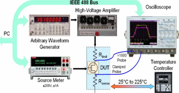
The hardware needed for the measurements include an Arbitrary Waveform Generator (AWG) for programmable pulse generation, a source meter for gate drive, a digital oscilloscope for data acquisition, a custom-made high-voltage amplifier, and a custom-made temperature-controlled high-voltage-isolated heat sink. The high voltage amplifier is controlled by the AWG, and provides the stimulus voltage for the device under test (DUT).
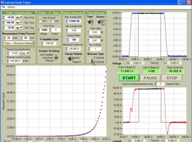
The curve tracer user interface is designed and implemented in LabWindows/CVI† instrument control environment. The curve tracer software mainly controls a high-voltage pulse that is applied to a SiC DUT and acquires the generated response. Some of the main attributes of the curve tracer program include a programmable one-shot pulse generation, automatic vertical and horizontal scaling of the oscilloscope for maximum resolution, programmable sampling rate, and current limit protection. The data for the I-V curve is acquired within the specified interval set by the user. Fig. 2 shows the curve tracer program user interface main panel.
Figure 2. Curve tracer user interface main panel.
†
LabWindows/CVI is a trademark of National Instruments Inc. Certain commercial products are identified in this paper to specify the experimental procedure adequately; nevertheless, this does not imply recommendation or endorsement by the National Institute of Standards and Technology.
Figure 3. Detail of the user interface main panel subdivisions. The user interface has three plotting areas. Two of them, located to the right side of the panel in Fig. 2, are dedicated to the current and voltage measurements of the DUT, and the third one, located at the bottom left corner of the panel, is for the I-V characteristics of the device. The curve tracer main user input panel is divided into the four different sections (shown in Fig. 3) that are described below.
A. The Applied Pulse Characteristics
In the Pulse Characteristics section, the user can define some parameters associated with the pulse applied to the DUT. The pulse signal generated by the AWG is composed of three independent but consecutive intervals identified as Rise Time, Flat Time, and Fall Time. These intervals allow the user to define different pulse sizes, as long as they are within the AWG hardware limits. For example, the pulse width cannot be less than 175 ns or greater than 0.5 s for the particular AWG used.
A better view of the user-defined pulse can be obtained if the user presses the [PulseÆPreview/Adjust] button. This brings up a secondary panel that contains more detailed information about the pulse shape and characteristics. This secondary panel is shown in Fig. 4. A plot in this secondary panel shows the user the approximate shape that the AWG pulse is sending to the DUT. Both the user interface main panel and this secondary panel share the settings for the Measurement Delay Percent interval limits. These limits are clearly seen in Fig. 4 as the two vertical lines intersecting the pulse shape.
The data measured within this time interval is used to compute the I-V values for every acquired pulse by averaging the data segment between the interval limits. The measurement interval limits are also shown overlapping each acquired pulse waveform as shown in the main panel of Fig. 2, and are displayed in the oscilloscope screen at the same locations. These lines can be manipulated even during run time, giving the user the flexibility to adjust the measurement interval width or location in case these settings are inadequate according to the behavior of the acquired waveforms.
Figure 4. [PulseÆ Preview/Adjust] panel.
For each measurement pulse, the data within the measurement interval for both the voltage and current pulses is averaged to form a I-V data point that is displayed in the left hand graph of Fig. 2 as it is obtained. The averaging function can be performed either by the oscilloscope or the curve tracer program. The user selects which averaging method to use with the Pulsed Waves Averaging option. The Pulse Duty control is used to set a measurement delay for the AWG pulse generation to prevent excessive device heating that consecutive pulses may produce.
B. Probes and Gains Settings
The Probes-&-Gains section shown in Fig. 3 is used to specify the parameters of the pulse generation and measurement circuits. When the user selects the Auto Sensed checkboxes the program uses the voltage probe gains that the oscilloscope senses from the probes in order to compute the I-V values with their correct magnitudes. Otherwise, the user must provide the specific User Given gains if the probes do not have auto-probe-gain-detection capability. When the gains are provided by the user, all signals will be acquired presuming that the probe gains are of magnitude ×1, and the given gains will be used by the program to correct the actual measurement gain.
The high-voltage pulse applied to the DUT is generated by amplifying the low-voltage (0 V ~ ±10 V) AWG pulse. Therefore, the user must provide the V Amplifier Gain value to the program. Several different amplifiers are presently used depending on the voltage measurement range required. For example, a high-power 30 V amplifier with a gain of ×2.57 is used for gate leakage measurements. For high-voltage drain or anode leakage measurements, a second amplification stage increases the total voltage gain close to ×1500, allowing the applied pulse to reach almost 15 kV. A higher gain first stage
amplifier can extend the range of the second stage to 25 kV which is the hardware capability of the system [7].
C. The Sweep Generator
The Sweep Generator section shown in Fig. 3 is used to specify the range and number of measurements to be performed. The user specifies the minimum and maximum measurement voltages that will be applied to the DUT using the Min Sweep Volts and Max Sweep Volts values, respectively. The Sweep Polarity setting is used to determine whether the low-voltage AWG pulse is generated from 0 V to +10 V or from 0 V to -10 V. The Sweep Points value specifies the number of measurements that will be performed between these two limits. The application uses these voltage limits in combination with the V Amplifier Gain value to generate the series of high-voltage pulses that will be applied to the DUT. The user can also specify a Maximum Current limit that is checked during the measurement process to avoid damaging the DUT from excessive current flow.
D. The Step Generator
The Step Generator section shown in Fig. 3 is used to specify bias steps that are applied to the DUT third terminal if required. The user selects the Measure Type option to be 3 Terminal for three terminal device types such as MOSFETs, IGBTs, and bipolar junction transistors. Diodes are an example of a 2 Terminal type device. The Type and Device options also provide more information about the device being tested, especially for the data and parameters that are saved for each measurement cycle file in the computer.
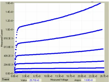
The 3 Terminal type tests are initialized by setting a Start Value for the first step gate voltage or base current, depending on the device being measured. In the case of power MOSFETs, the gate signal will be an applied voltage, while bipolar transistors use an applied current bias. The number of curves that will be generated after this initial point is given by the No. of Steps value. The Step Change value specifies the increment or decrement amount by which each consecutive step will change the previous bias level. The test will end when the specified amount of steps is reached or when the Maximum Current limit is reached during the measurement process, whatever occurs first. As an example, Fig. 5 shows an acquired family of curves obtained for a low-voltage commercial silicon MOSFET used to test the Step Generator section.
E. Other Oscilloscope-Related Parameters
The program allows the oscilloscope to adjust the vertical gains of its channels depending on the Scope Scaling option specified by the user below the Probes-&-Gains section in Fig. 3. The oscilloscope normally uses fixed vertical gains in multiples of 1, 2, and 5 voltage units-per-division.
Figure 5. Example of I-V curves acquired from a commercial silicon MOSFET during a Measure Type: 3 Terminal test.
This will be specifically set if the user selects the Auto-Fixed scaling option. If the Auto-Variable option is selected, the oscilloscope will maximize the acquired waveforms screen view as much as possible by setting vertical gains for each channel in magnitudes that differ from the default 1-2-5 voltage units-per-division. Programmed maximum and minimum screen limits specify how the acquired waveforms will be displayed in both -Fixed and -Variable options. The Manual option allows the oscilloscope gains to be set manually by the user as desired, and the signals will be acquired just as they are displayed in the oscilloscope screen. The program uses the size of the user-defined AWG pulse to automatically set the oscilloscope horizontal scaling. The pulse response to be captured by the oscilloscope starts at the first horizontal screen division.
The acquired waveform is zoomed in as much as possible as long as the following conditions are satisfied: 1) the base of the signal should be one screen division up from the bottom of the screen; 2) the pulse should have its measurement interval as close as possible to the top but never more than six divisions above the division used for the base; and 3) the whole pulse width should fit within the screen view without going beyond the right-most edge of the screen.
This last condition is met by keeping the right edge of the pulse typically between the fifth and eighth horizontal oscilloscope screen divisions (ten divisions make up the horizontal screen width). Since the application focuses mostly on keeping the averaged waveform value between all these visual limits, some peaks or oscillations can be clipped off in the acquired measurements, but they are outside the measurement interval that is averaged to calculate each I-V data point.
The current flowing through the DUT is measured by acquiring the terminals voltage of a sensing resistor located in the testing circuit shown in Fig. 1. The user must specify the value of this resistive component through the Current Sensing Resistor parameter value below the Pulse Characteristics section in Fig. 3. The program will compute the actual DUT
current value by dividing the measured sensing resistor voltage by the given sensing resistor value. The program also calculates the actual DUT voltage by subtracting the voltage measured at the device drain terminal from the voltage value measured at the current sensing resistor (see Fig. 1). The low voltage current sensing probe is provided with protection clamp elements to prevent high voltage from damaging the oscilloscope in the event of DUT failure. The user can also set a certain Minimum Current Scaling value in order to prevent the instrument from scaling below the noise floor for the current sensing resistor measurement, when appropriate. F. User Control and System Feedback
While the program is running, some of the measurement values are continuously shown to the user through their respective interface controls. Fig. 6 shows the location of such controls in the main panel. The approximate Pulse Voltage value that is being applied to the DUT is always shown during runtime. If the measurement is for a 3 Terminal type test, the Gate Voltage value for each curve trace is shown while it is being measured. The source generator that applies this signal can also show the user the Gate Current value being drawn from the device. The term Gate is being used in this case from the presumption that the device being tested is a MOSFET, but the captions will be Base Voltage and Base Current in the event that the device being measured is a bipolar junction transistor, for example.
During the measurement process the user can use the mouse cursor to pinpoint any location on any of the plots, and the corresponding (X, Y) coordinate values at that point will be displayed in their respective boxes below each plot. The user can also specify that the voltage and current pulse waveforms be saved after each pulse is applied to the device so that they can be analyzed later after the measurement sequence is completed. The Auto-Save Measurements every n Sweep Points data entry field (at the bottom of Fig. 6) enables the user to specify that the pulse waveform data be saved only when every n-th pulse is applied. Thermal effects and erratic breakdown can be evaluated from the shape of these saved current pulse waveforms.
Finally, the menu bar options available in the user interface main panel (top of Fig. 1) allow the user to perform basic procedures like loading previously saved parameters for a certain test or device, save traces or waveforms, select color options for the traced curves points, change the plots background colors, or set other miscellaneous preferences.
III. GENERAL MEASUREMENT PROCEDURE
A typical SiC power device test consists of a series of steps and decisions that the user must take to perform the measurement. First, the user must make all the necessary instrument and test bed connections to the DUT. The user can load a series of previously saved configuration parameters from a file that may be used for measurement uniformity purposes, or the user can input new configuration parameters such as gain and sensing resistor values. Any specific test can be repeated at different temperatures to analyze the electro-thermal behavior of the DUT. Although precise thermal control is another of the features of the custom-made test bed, the actual temperature controller being used is not part of the instruments managed by the curve tracer program. A description of how the 25 kV voltage-isolated temperature-controlled heat sink is operated and adjusted through feedback from the test bed is presented in [7].
Once all configuration tasks are fulfilled, the test can be initiated by pressing the [START] button. As the program starts, the pulse shape is loaded into the AWG. This pulse loading will only occur if the measurements are being done for the very first time since the application was loaded, or whenever the application detects that the user changed the pulse characteristics for a new test. If no changes were made to the pulse, AWG pulse loading will not occur after [START] is pressed. If the test is a three-terminal type, the source generator will apply the first gate (or base) bias level. The program will ask for an optional filename to save measurement waveform data every n-th pulse during the measurement sequence if the Auto-Save Measurements every n Sweep Points option shows an n value other than zero.
Next, the program makes the vertical scale adjustments on the oscilloscope (if set to other than manual) until the waveforms are auto-scaled to fit within its screen size for each measurement point. Finally, the waveforms are transferred from the oscilloscope to the computer, averaged within the
range specified by the user to determine the I-V data point, and this data point is displayed on the bottom left graph shown in Fig. 2.
As the measurement sequence proceeds, the scales continue to adjust as the applied power pulse change according to the given amount of points and the voltage limits. The user can pause the process at any time without losing the already acquired data with the [PAUSE] button. This allows the user to analyze the acquired waveforms or make any necessary instrument adjustments. The [START] button becomes a [RESUME] button in this case to inform the user that the process can be resumed after the pause.
Once the measurement sequence is completed (maximum voltage or current limit is reached), a popup message asks the user to save or discard the measured I-V data that has been temporarily stored during the process. Figs. 7 to 11 show examples of different measurements that have been obtained at NIST for SiC HV-HF devices.♣ The tests were done at various temperatures to reveal the electro-thermal behavior of each DUT.
IV. CONCLUSION
A software-based HV-HF curve tracer application for SiC device characterization has been presented. The flexibility of the curve tracer user interface proves effective to perform different high-voltage leakage measurements for SiC MOSFETs and PiN diodes, and also for gate leakage in the MOSFETs at different temperatures. There is no single commercial instrument at this moment capable of performing the same procedures used to acquire the presented measurement results. Therefore, the software-based curve tracer presented in this paper provides a valuable tool for the evaluation of future HV-HF SiC power devices.
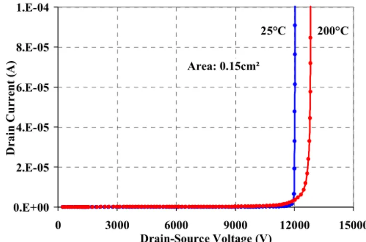
0.E+00 2.E-05 4.E-05 6.E-05 8.E-05 1.E-04 0 3000 6000 9000 12000 15000 Drain-Source Voltage (V) D r ai n C u rrent ( A ) 25°C 200°C Area: 0.15cm²
Figure 7. A SiC MOSFET drain leakage measurement at 25°C and 200°C.
x
♣ The devices shown in this paper were produced by Cree Inc. under the DARPA WBST HPE Phase 3 program sponsored by Sharon Beermann-Curtin and monitored by Harry Dietrich.
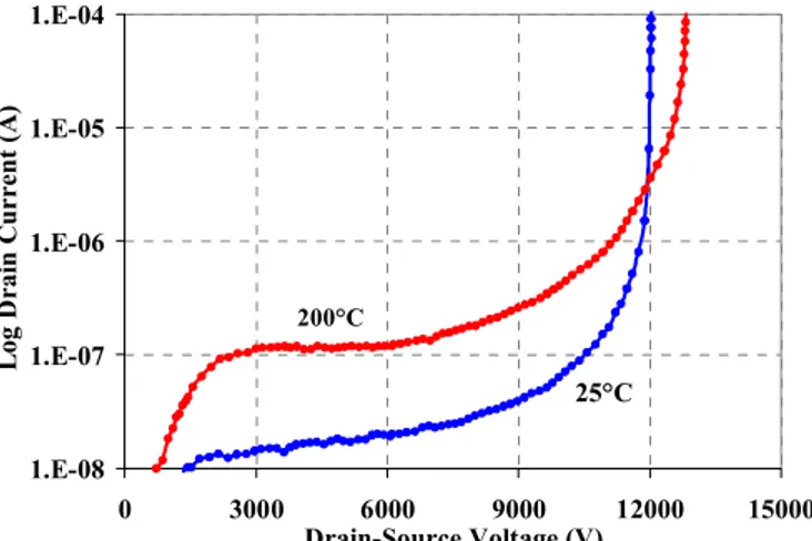
1.E-08 1.E-07 1.E-06 1.E-05 1.E-04 0 3000 6000 9000 12000 15000 Drain-Source Voltage (V) L og D r ai n C u rrent ( A ) 25°C 200°C
Figure 8. Semi-log plot of the measurements shown in Fig. 7.
-1.E-05 0.E+00 1.E-05 2.E-05 3.E-05 4.E-05 5.E-05 6.E-05 7.E-05 8.E-05 0 3000 6000 9000 12000 15000 Voltage (V) C u r r e n t (A ) 25°C
Figure 9. Linear plot of a reverse anode leakage test for a SiC PiN diode showing a measured breakdown of approximately 13.5 kV at 25°C.
1.E-10 1.E-09 1.E-08 1.E-07 1.E-06 1.E-05 1.E-04 0 3000 6000 9000 12000 15000 Voltage (V) C u r r e n t (A ) Area: 0.2 cm² 200°C 175°C 150°C 25°C
Figure 10. Semi-log plot of different temperature effects on the DUT response for Fig. 9. 0.0E+00 2.0E-09 4.0E-09 6.0E-09 8.0E-09 1.0E-08 1.2E-08 1.4E-08 1.6E-08 1.8E-08 2.0E-08 0 3 6 9 12 15 18 21 24 27 Gate-Source Voltage (V) G a te C u r r e n t (A ) 200°C 150°C 100°C Area: 0.15cm² {10kV, 5A} 25°C 50°C
Figure 11. Gate leakage response for a SiC MOSFET at different temperatures.
REFERENCES
[1] S. Beermann-Curtin, et al., “Development of SiC high power electronics for naval aircraft carriers,” in 30thGOMACTech Conf., pp. 218-221, Las Vegas, NV, April 2005.
[2] Defense Advanced Research Projects Agency (DARPA), Microelectronic Technology Office (MTO), Wide Bandgap Semiconductor Technology High Power Electronics Program (WBG-HPE): http://www.darpa.mil/mto/solicitations/ BAA # 06-30.
[3] A.R. Hefner, D. Berning, C. Ellenwood, “Metrology for high-voltage, high-speed silicon carbide power devices,” in 30thGOMACTech Conf., pp. 226-229, Las Vegas, NV, April 2005.
[4] A.R. Hefner, T. McNutt, A. Akuffo, R. Singh, C. Ellenwood, D. Berning, M.K. Das, J.J. Sumakeris, and R. Stahlbush, “Characterization of SiC PiN diode forward bias degradation,” in Recs. 39thIEEE Ind. Apps. Conf. vol. 2, pp. 1256-1260, Seattle, WA, October 2004.
[5] A. Hefner, “Status of high-voltage, high-frequency silicon-carbide power devices,” in 31st GOMACTech Conf., pp. 232-235. San Diego, CA, March 2006.
[6] A. Hefner, S-H Ryu, B. Hull, D. Berning, C. Hood, J.M. Ortiz-Rodríguez, A. Rivera-Lopez, T. Duong, A. Akuffo, and M. Hernandez-Mora, “Recent advances in high-voltage, high-frequency silicon-carbide power devices,” to appear in Recs. 41st IEEE Ind. Apps. Conf., Tampa, FL, October 2006.
[7] D. Berning, A. Hefner, J. M. Ortiz-Rodríguez, C. Hood, and A. Rivera “Generalized test bed for high-voltage, high-power SiC device characterization,” to appear in Recs. 41st IEEE Ind. Apps. Conf., Tampa, FL, October 2006.
![Figure 4. [PulseÆ Preview/Adjust] panel.](https://thumb-eu.123doks.com/thumbv2/9libnet/5643933.112320/3.918.67.450.80.404/figure-pulseæ-preview-adjust-panel.webp)