Nanotechnology
PAPER
Cubic-phase zirconia nano-island growth using
atomic layer deposition and application in
low-power charge-trapping nonvolatile-memory
devices
To cite this article: Nazek El-Atab et al 2017 Nanotechnology 28 445201
View the article online for updates and enhancements.
Related content
One versus three-dimensional quantum confinement in 1–5 nm ZnO nanoparticle agglomerations for application in charge trapping memory devices
Nazek El-Atab and Ammar Nayfeh
-Improved Operation Characteristics for Nonvolatile Charge-Trapping Memory Capacitors with High- Dielectrics and SiGe Epitaxial Substrates
Zhao-Zhao Hou, Gui-Lei Wang, Jin-Juan Xiang et al.
-A M-AZOS structure for high-performance non-volatile memory application
Jing Liu, Qin Wang, Shibing Long et al.
Cubic-phase zirconia nano-island growth
using atomic layer deposition and
application in low-power charge-trapping
nonvolatile-memory devices
Nazek El-Atab
1,6, Turkan Gamze Ulusoy
2,3, Amir Ghobadi
3,4, Junkyo Suh
5,
Raisul Islam
5, Ali K Okyay
2,3,4, Krishna Saraswat
5and Ammar Nayfeh
1,6 1Department of Electrical Engineering and Computer Science(EECS), Masdar Institute of Science and Technology Abu Dhabi, United Arab Emirates
2
Institute of Materials Science and Nanotechnology, Bilkent University, 06800 Ankara, Turkey 3
UNAM-National Nanotechnology Research Center, Bilkent University, 06800 Ankara, Turkey 4
Department of Electrical and Electronics Engineering, Bilkent University, 06800 Ankara, Turkey 5Department of Electrical Engineering, Stanford University, CA, United States of America
E-mail:[email protected]@masdar.ac.ae
Received 3 July 2017, revised 15 August 2017 Accepted for publication 23 August 2017 Published 5 October 2017
Abstract
The manipulation of matter at the nanoscale enables the generation of properties in a material that would otherwise be challenging or impossible to realize in the bulk state. Here, we demonstrate growth of zirconia nano-islands using atomic layer deposition on different substrate terminations. Transmission electron microscopy and Raman measurements indicate that the nano-islands consist of nano-crystallites of the cubic-crystalline phase, which results in a higher dielectric constant(κ∼35) than the amorphous phase case (κ∼20). X-ray photoelectron spectroscopy measurements show that a deep quantum well is formed in the Al2O3/ZrO2/Al2O3 system, which is substantially different to that in the bulk state of zirconia and is more favorable for memory application. Finally, a memory device with a ZrO2nano-island charge-trapping layer is fabricated, and a wide memory window of 4.5 V is obtained at a low programming voltage of 5 V due to the large dielectric constant of the islands in addition to excellent endurance and retention characteristics.
Supplementary material for this article is availableonline Keywords: zirconia, atomic layer deposition, memory devices (Some figures may appear in colour only in the online journal) Nanoscale materials often exhibit significantly different properties to those in their bulk state. The distribution of nanoscale materials on large areas provides a route towards functional materials with novel properties[1–3]. These pro-mising properties have enabled new technologies, including nanoscale lasing schemes [4, 5], memory devices [6, 7], sensitive detection devices[8–10], and improved photovoltaic
sensitivities [11]. Further progress towards achieving new nanomaterial properties necessitates the ability to grow the nanoparticle constituents on different substrate terminations to meet the requirements of different applications.
In addition to its various applications in fuel cells [12], dentistry [13], the aviation industry [14], nanoelectronics [15], etc, ZrO2is widely used as a high-κ material in dynamic random access memory (DRAM) as well as for MOS gate oxides[16]. In fact, ZrO2is projected to be the key material in Nanotechnology
Nanotechnology 28(2017) 445201 (10pp) https://doi.org/10.1088/1361-6528/aa87e5
6
Authors to whom any correspondence should be addressed.
sub-20 nm DRAM generation [17]. However, deep knowl-edge of ZrO2 thin-film characteristics, especially of the electronic and structural properties, is critical to meet the requirements of future devices. In addition, high-κ materials are preferred to be used in the charge-trapping layer of memory devices, since this will increase the electric injection field and, therefore, a lower operating voltage can be achieved [18]. ZrO2-based dielectrics are a promising candidate for this since they can be crystallized into cubic and tetragonal phases with large dielectric constants (κ-values of ∼35 and ∼46, respectively) [19]. However, it is commonly believed that an amorphous material would be more suitable for a memory charge-trapping layer since grain boundaries existing in crystalline materials can provide leakage paths and deteriorate the retention characteristic of the memory[19]. At the same time, amorphous ZrO2has a lower dielectric constant(∼20) than the crystalline phases, which would result in a lower injectionfield and thus a higher required operating voltage. Therefore, there would be a trade- off between the retention characteristic and operating voltage of the memory. One solution would be to use nano-islands/nano-crystals in the charge-trapping layer instead of a continuous crystalline layer, so that the leakage probability is reduced since only the nano-crystallites above the defects in the tunnel oxide would leak, and thus the retention would be improved without sacrificing the large dielectric constant of the crystalline material.
In addition, atomic layer deposition(ALD) is currently being extensively used in industry to deposit conformal thin films for various nanoelectronic applications where any dis-continuity in the film would cause reliability issues such as leakage paths in the gate oxide of transistors. Other applica-tions require nano-island growth such as in light-trapping schemes for increasing solar cells’ efficiency. Therefore, it is crucial to understand the deposition conditions in ALD that lead to nano-island growth instead of continuous thin-film growth on different substrate terminations.
In previous work, island growth has been observed on hydrogen (–H)-terminated Si substrates, which are obtained when the Si is pretreated with hydrofluoric (HF) acid to remove the native oxide[20,21]. However, some applications require the deposition of ZrO2on hydroxyl(–OH)-terminated substrates or Al2O3as in the case of charge-trapping memory devices. Here, we show that zirconia nano-islands can also be grown on Si substrates with–OH termination and on Al2O3 thinfilms. The effect of the substrate termination on the size and density of the nano-islands is also studied. In addition, it has been previously demonstrated that growth in ALD during thefirst few cycles follows the Volmer–Weber (VW) growth mode where the deposition happens on the active sites of the substrate resulting in nano-islands and, as the number of cycles increases, the islands start to merge and form a con-tinuous layer [22]. In this work, we show that nano-islands can also be formed during ALD deposition due to the diffu-sion and agglomeration of the adsorbed atoms (adatoms) when the temperature is high enough to provide the adatoms with the energy needed to diffuse, resulting in thicker nano-islands than in the case of VW growth. The electronic and
structural properties of the nano-islands grown are char-acterized using different tools such as atomic force micro-scopy (AFM), transmission electron microscopy (TEM), Raman spectroscopy, and UV–vis–NIR spectrophotometer. Specifically, we demonstrate that the zirconia nano-islands consist of nano-crystallites of the cubic phase and, therefore, result in a higher dielectric constant in addition to having a large band offset with Al2O3. In addition, a memory device with zirconia nano-islands as the charge-trapping layer is fabricated for the first time and the results show that a low operating voltage can be achieved with excellent retention and endurance characteristics, making the nano-islands pro-mising in low-power memory application.
Nano-island deposition and physical characterization
The deposition of the ZrO2nano-islands is conducted using thermal ALD on p-type Si substrates. The ALD system is an S200 Savannah ALD and the precursors are Tetrakis (dime-thylamido)zirconium(IV) and H2O. Firstly, the Si substrates are treated in a piranha solution at 120°C for 20 min to remove any organic contamination followed by 30 s dip in 50:1 DI:HF solution to remove the native oxide. Then, the substrates are inserted into the ALD chamber and a deposition of 20, 30 and 40 cycles of ZrO2 is conducted at 150°C, 200°C, and 250 °C. The deposition process consists of the following steps: a pulse of the zirconium precursor for 300 ms followed by a N2-purging step for 20 s, then the H2O pre-cursor is added for 15 ms followed by a N2-purging step for 20 s, during which the chamber pressure is 300 mTorr. In addition, in order to understand the effect of the substrate termination on the islands’ growth mechanism, the same deposition of the ZrO2 cycles is conducted on Si substrates with only piranha treatment (i.e. without HF treatment), and Si substrates with piranha and HF treatment followed by deposition of 4 nm Al2O3thin film by ALD.
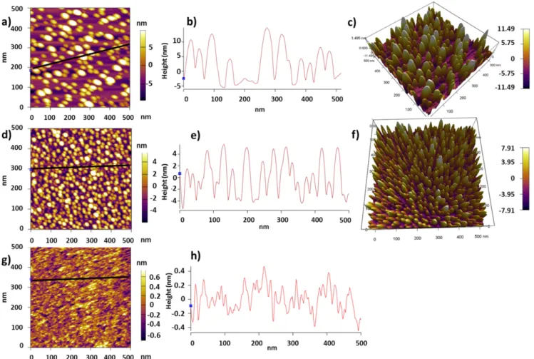
AFM(AC-in-air mode) is first used to characterize the size and density of the nano-islands. The substrate with only pir-anha treatment(–OH termination) showed ZrO2nano-islands with less than 30 nm width and thickness ranging from 10 to 20 nm(figures1(a)–(c)) after 20 cycles of deposition at 250 °C, while after 30 cycles, the number of nano-islands increased, but their size was reduced so that the width is less than 10 nm and the thickness is around 8 nm(figures1(d)–(f)). Moreover, after 40 cycles of deposition, a 2.9 nm continuousfilm was obtained with an RMS roughness of around 0.35 nm(figures1(g)–(h)). Therefore, it is observed that the islands are first larger and then, as the number of cycles is increased, their size is reduced but their density is increased, until a thinner continuousfilm (compared to that of islands) is obtained.
The steady-state ALD deposition rate of continuous ZrO2 thin film under the same conditions is known to be ∼0.8 A°/cycle; however, the size of the islands obtained with 20 and 30 ALD cycles is much larger (>∼7 nm) and the sizes of the islands are also different, which indicates that they were not grown at the same time. In fact, the
growth mode can be understood by considering the ther-modynamic tendency of a system to minimize its total energy[23]. Since the surface atoms are bound less tightly, they are more energetic than the bulk atoms in the same structure. This energy increase is known as ’surface free energy’. The surface free energy tends to be reduced when the surface area is minimized. This phenomenon is respon-sible for common effects such as droplet formation and capillary action [23]. In addition, at lower deposition tem-peratures of 150 and 200°C, no islands were observed, which further confirms this analysis. Therefore, when the temperature is high enough, the adatoms or surface atoms gain enough energy to diffuse on the surface and agglom-erate to reduce the total energy of the system, resulting in large islands. Another phenomenon that is needed to understand the growth mechanism is the stress evolution during growth. Stress evolution during island growth has been well studied in the past, and it has been shown that a compressive stress isfirst generated in the islands and then, as the islands get closer to each other, a tensile stress develops, which is explained by the stretching of the islands to close the gap between each other and reduce the total energy of the system. Finally, when the islands have coa-lesced, the stress becomes compressive again [24, 25].
Therefore, in our fabricated nano-islands, as the number of cycles is increased, the number of islands is increased and the spacing in between them is reduced. Therefore, the islands will stretch to close the gap between each other and reduce the total energy of the system, resulting in smaller number of larger-sized islands until a continuous thinfilm is obtained, as shown infigure1(g). In fact, with 30 cycles, the islands start to merge, so their bottom forms a larger island base, but their top consists of smaller islands. And since the AFM image shows the topography of the top islands and not their base, smaller islands are observed on the AFM 2D images with 30 cycles than with 20 cycles(figure1(d)). This can also be seen in the line-section image of the islands obtained using the AFM tool(figure1(e)), which shows how the islands’ bases merged, resulting in thinner top islands with smaller widths.
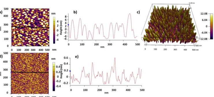
On the Si with–H termination, after 20 cycles, the observed number of islands is larger than in the case of Si with –OH termination, and the thickness ranges from 6 to 12 nm while the width is less than 15 nm (figures 2(a)–(c)). After 30 cycles, a continuous 2.8 nm thinfilm is obtained with an RMS roughness of around 0.28 nm (figures2(d)–(e)). The reason for the larger number of islands observed in the case of the–OH-terminated substrate after the same number of cycles can be explained by
Figure 1.AFM characterization of the nano-islands deposited on–OH-terminated Si at 250 °C: (a) 2D AFM image of 20 ALD cycles of ZrO2.(b) Line cross-section across the black line shown in (a). (c) 3D AFM image of the nano-islands shown in (a). (d) 2D AFM image of 30 ALD cycles of ZrO2.(e) Line cross-section across the black line shown in (d). (f) 3D AFM image of the nano-islands shown in (d). (g) 2D AFM image of 40 ALD cycles of ZrO2.(e), Line cross-section across the black line shown in (g).
3
the–H termination. In fact, –H termination plays the role of a surfactant that affects thefilm growth by modifying its kinetics [26]. In this case, the surfactant reduces the adatom mobility on the substrate resulting in a higher density of islands. Indeed, the reduction of the adatom mobility is known to improve the 2D
growth offilms because it results in a higher density of nano-islands[26].
On Al2O3, the growth is similar to that of the –OH-terminated substrate since the ALD deposition of Al2O3film is ended with a H2O dose/purge cycle, which results in
Figure 2.AFM characterization of the nano-islands deposited on–H-terminated Si at 250 °C: (a) 2D AFM image of 20 ALD cycles of ZrO2. (b) Line cross-section across the black line shown in (a). (c) 3D AFM image of the nano-islands shown in (a). (d) 2D AFM image of 30 ALD cycles of ZrO2.(e) Line cross-section across the black line shown in (d).
Figure 3.AFM characterization of the nano-islands deposited on Al2O3at 250°C.: (a) 2D AFM image of 20 ALD cycles of ZrO2.(b) Line cross-section across the black line shown in(a). (c) 3D AFM image of the nano-islands shown in (a). (d) 2D AFM image of 30 ALD cycles of ZrO2.(e) Line cross-section across the black line shown in (d). (f) 3D AFM image of the nano-islands shown in (d). (g) 2D AFM image of 40 ALD cycles of ZrO2.(e) Line cross-section across the black line shown in (g).
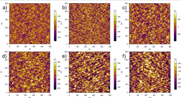
a –OH-terminated surface. However, due to the different properties of the substrate, the resulting deposition rate is different and, therefore, the sizes of the islands are different as well. But the trend is similar to the case of Si with –OH termination where fewer islands are obtained after 20 cycles of deposition in comparison to the –H-terminated sample. After 20 cycles, islands with a width of less than 25 nm are obtained with a 4–12 nm thickness (figures 3(a)–(c)), while after 30 cycles, more islands are obtained with smaller sizes where the width is less than 10 nm and the thicknesses range is 4–6 nm (figures 3(d)–(f)). Finally, after 40 cycles of deposition, a continuous film is obtained with a 2.5 nm thickness and an RMS roughness of around 0.3 nm (figures 3(g)–(h)). Finally, it is worth mentioning that no islands are observed at temperatures lower than 250°C for all three substrates.
Therefore, it can be confirmed that the nature of the growth is affected by many factors, including substrate temperature, film and substrate species/termination, and deposition energy and rate. Overall, we can summarize this as follows: when surface diffusion/adatom mobility is high and the deposition rate is low, which occur at high deposition temperatures, then the nucleation density is low and larger islands form.
At temperatures of 150°C and 200 °C, no islands were observed; instead, a continuous thin film was obtained. The AFM topography for the samples with 20, 30 and 40 cycles deposited at 150°C are shown in figures 4(a)–(c), respec-tively, and the AFMfigures for the samples with 20, 30, and 40 cycles deposited at 200°C are shown in figures4(d)–(f), respectively. It is clear from thefigures that continuous films are obtained with a small RMS roughness (less than 1 nm)
and, in addition, smaller grains are obtained with 150°C than with 200°C, as expected. The measured thicknesses for the thin films obtained are 1.96 nm, 2.94 nm, 3.92 nm, 1.72 nm, 2.58 nm, and 3.44 nm, respectively, for the films shown in figures 1(a)–(f).
Structural and optical characterization of the nano-islands
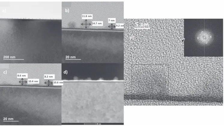
TEM analysis is conducted for nano-islands grown on substrate with–H termination (pretreated with HF) after a deposition of 20 ALD cycles. The TEM images were obtained using an FEI TECNAI TF-20 FEG/TEM operated at 200 kV in bright-field TEM mode (figure 5(a)), high-resolution TEM mode (figures5(a), (c), (e)), and high-angle annular dark-field STEM (scanning transmission electron microscope) mode (figure5(d)). The STEM probe size was 1–2 nm in nominal diameter. The TEM images show that the island thickness is in the range of 7–12 nm and the width is in the range of 9–15 nm, which is consistent with the AFM results provided above. In addition, the TEM image shows that the nano-islands are polycrystalline, as indicated by the fast Fourier transformation (FFT) pattern showing clear rings(figure5(e)). Moreover, TEM images show an interdiffusion layer which consists of the elements S, O, and Zr. This interdiffusion layer is thinner below the islands (figure 5(d)) since little interdiffusion is expected under a crystalline material due to the limited solid solubility in equi-librium. While in the areas in between the islands, which are exposed to ambient air, the oxygen can diffuse through this layer, resulting in a thicker interdiffusion layer[27].
Figure 4.AFM topography of the zirconia samples obtained with(a) 20 ALD cycles at 150 °C, (b) 30 ALD cycles at 150 °C, (c) 40 ALD cycles at 150°C, (d) 20 ALD cycles at 200 °C, (e) 30 ALD cycles at 200 °C, and (f) 40 ALD cycles at 200 °C.
5
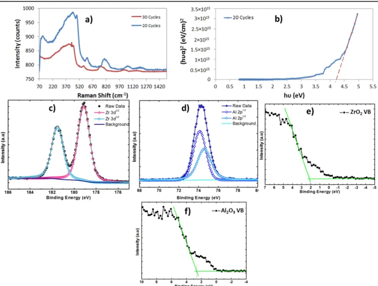
In order to determine the crystalline phase available in the islands, Raman measurements are conducted on the samples with 20 and 30 ALD cycles(figure6(a)). The cubic-phase zirconia is characterized by broad bands[28] centered at 246, 301, 436, and 625 cm−1. Our measurements for the sample with 20 cycles show peaks at 448, 490, 610, and 815 cm−1, which are roughly the version of the cubic-phase peaks blue-shifted by 200 cm−1 while the 30-cycle sample results in peaks blue-shifted by around 160 cm−1. This shift is explained by a compressive stress in the material[29]. This is expected since, with 20 cycles, the islands are still isolated, spaced and have still not coalesced, as shown in the TEM images. Therefore, they are supposed to be experiencing compressive stress, as already explained in thefirst section. With 30 cycles, however, the island bottoms have already merged and coalesced, which is explained by the smaller widths and thicknesses measured for the islands(figures1(d)– (f)). Therefore, the film would be experiencing compressive stress again. Moreover, the Raman signal intensity is different between 20 and 30 cycles since it depends on the thickness and roughness of thefilm: thicker and rougher films result in stronger signal intensity[30].
Thus, the dielectric constant of the nano-islands is expected to be around 35, which is the known dielectric constant of cubic-phase zirconium dioxide[19]. This high-κ value is favorable for the charge-trapping layer of memory devices since it will boost the electricfield injection leading to a lower-power memory. Transmittance and reflectance
measurements are also conducted using the UV–vis–NIR spectrophotometer and the Kubelka–Munk function is used to extract the bandgap of the nano-islands (figure 6(b)). The function plots (ɦυα) 2 versus ɦυ, where ɦυ is the photon energy and α is the absorption coefficient [31–33]. The extracted bandgap value is around 4.2 eV, which is consistent with the cubic-phase bandgap [28].
To understand the electron transfer processes and charge transfers in the ZrO2 nano-islands deposited on the Al2O3 structure, the valence and conduction band offsets (ΔEv and ΔEc) are extracted using XPS measurements, as explained in [34]. In this technique, ΔECLis the energy difference between the Zr3d and Al2p core levels (CLs) in the Al2O3/ZrO2 het-erojunction, as shown in Fig S1a–b and ΔECL is found to be 107.85 eV. The energy difference between the CL and the valence-band maximum(VBM) for bulk ZrO2(ECL-EVBM)ZrO2 is determined to be 176.92 eV [35], while this value for bulk Al2O3(ECL-EVBM)Al2O3is 71.42 eV[36]. Here, the calculated EVBM values are 2.2 eV and 2.7 eV for ZrO2 and Al2O3, respectively(see figures6(e)–(f)). It should be noted that the CL spectra of Zr3d5/2and Al2p3/2show peaks located at 182.13 eV and 74.28, respectively. All results obtained are summarized in table1. The optical bandgap of the cubic-phase ZrO2estimated from the Kubelka–Munk graph is 4.2 eV, as mentioned above. The bandgap of Al2O3 is 6.8 eV at room temperature [37]. Finally,ΔEVandΔEC are calculated as 2.35 eV and 4.95 eV, respectively.
Figure 5.TEM characterization of the 20-cycle nano-islands deposited on–H terminated at 250 °C: (a) Bright-field TEM mode showing the nano-islands.(b) High-resolution TEM mode showing the size of the islands. (c) High-resolution TEM mode showing the size of different islands.(d) High-angle annular dark-field STEM mode. The STEM probe size was 1–2 nm in nominal diameter. (e) High-resolution TEM mode showing the polycrystalline nature of the island and the FFT pattern showing circular rings and dots.
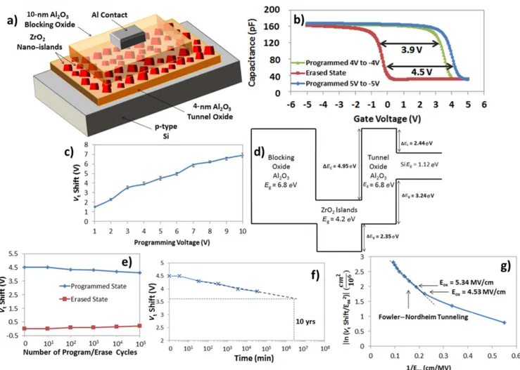
Fabrication and characterization of memory device with a ZrO2nano-island charge-trapping layer On highly doped p-type substrates, 4 nm Al2O3tunnel oxide is deposited by ALD at 250°C followed by 20 ZrO2cycles,
which results in zirconia nano-islands with thicknesses of 4–12 nm. The nano-islands form the charge-trapping layer. Then, a 10 nm Al2O3blocking oxide is deposited by ALD at 250°C, followed by the deposition of Al contacts using e-beam evaporation and a shadow mask to form the patterns (80×80 μm2). The cross-sectional illustration of the fabri-cated memory is depicted in figure 7(a). High-frequency (1 MHz) capacitance–voltage (C–V ) measurements are con-ducted on the memory devices: first, a programming gate voltage of 5 V is applied for 1 s and the gate voltage is then swept from 5 to−5 V. The C–V curve obtained corresponds to the programmed state. Then, a−5 V gate voltage is applied for 1 s and the gate voltage is swept from−5 V to 5 V which results in the erased state (figure 7(b)). A large memory window of around 4.5 V is obtained at this low program/ erase voltage (P/E), which can be explained by the high electricfield across the tunnel oxide due to the large dielectric constant of the cubic-phase zirconia. In addition, by pro-gramming and erasing the memory at different voltages, it is shown that large memory windows can be obtained at low operating voltages such as 3.9 V at 4/−4 V P/E reaching up to 7 V at 10/−10 V P/E (figure 7(c)). The error bars for
Figure 6.Optical and electronic characterization of the 20-cycle nano-islands deposited on Al2O3at 250°C. (a) Raman spectrum of the nano-islands.(b) Kubelka–Munk plot showing the bandgap of the nano-islands. (c) XPS peaks of the ZrO2islands.(d) XPS peaks of the Al2O3 background.(e) Valence band of the ZrO2islands.(f) Valence band of the Al2O3background.
Table 1.XPS parameters for band alignment between ZrO2 nano-islands and Al2O3.
Sample Region Binding Energy(eV)
Bulk ZrO2 Zr3d5/2 179.12 VBM 2.20 (ECL-EVBM) 176.92 Bulk Al2O3 Al2p 3/2 74.12 VBM 2.70 (ECL-EVBM) 71.42 ZrO2/Al2O3 Zr3d5/2 182.13 Al2p3/2 74.28 ΔEV(eV) 2.35 ΔEc(eV) 4.95 7 Nanotechnology 28(2017) 445201 N El-Atabet al
n=20 memory cells depicted in the figure confirm that the shift in the measured values is negligible, which could be due to the large number of islands in each memory device. In scaled devices, the physical gate length is projected to be around 100 nm for the next couple of years [17] and from figures 3(a) and (d), there will definitely be several nano-islands embedded in each memory cell; therefore, these devices are expected to be scalable.
In addition, the charge-trap state density in the nano-islands is calculated using the following equation[38–42]:
Nt 1 C V q t t = ´ D ( )
where Ctis the capacitance of the MOS memory with nano-islands per unit area(obtained from the C–V curves), V t∆ is the threshold-voltage shift, and q is the elementary charge. Nt of the ZrO2 nano-islands is found to be 1.2×1014cm−2, which is almost two orders higher than the reported trap-state density in ZrO2 continuous thin films deposited by ALD[43,44].
In additional, in our previous work, a memory with zinc-oxide(ZnO) nano-islands was demonstrated; however; due to the much higher dielectric constant of the cubic-phase ZrO2 nano-islands, a lower operating voltage is achieved whereby a 4 V memory window can be obtained at roughly 4/−4 V P/E voltages with ZrO2 while 6/−6 V P/E voltages would be required with ZnO nano-islands [45]. In addition, it is observed from the C–V curves (figure7(b)) that the memory is being programmed by storing electrons in the islands and is being erased by removing the electrons from the charge-trapping layer(figure7(b)). This is observed from the fact that the C–V curve corresponding to the erased state of the memory is the same at different erase voltages while the C–V curve corresponding to the programmed-state shifts to the right at higher program voltages, indicating that more elec-trons are stored in the nano-islands. The energy-band diagram of the memory structure is also constructed, and a deep quantum well is formed by the conduction bands of ZrO2 embedded in between the Al2O3 layers (figure 7(d)). This deep quantum well allows for the storage of electrons, while there is no quantum well formed by the valence bands of the
Figure 7.Characterization of the MOS memory device with a 20-cycle ZrO2nano-island charge-trapping layer:(a) Cross-sectional illustration of the fabricated memory device.(b) C–V characteristic of the memory programmed and erased at 5/−5 V and 4/−4 V. (c) Average of the measured Vtshifts at different program/erase voltages: error bars are included for n=20. (d) Energy-band diagram of the memory across a nano-island.(e) Endurance characteristic of the memory up to 105program/erase cycles. (f) Retention characteristic of the memory extrapolated up to 10 years.(g) Energy-band diagram of the memory across a nano-island showing the bandgaps of the different material(Eg).
layers, which may inhibit the storage of holes and cause their easy leakage. This confirms the observed program/erase mechanism of the memory, only storing and removing elec-trons from the charge-trapping layer. Moreover, the endur-ance characteristic of the memory is studied by programming and erasing the cells at 5/−5 V up to 105cycles while noting the change in the threshold-voltage (Vt) shift. The results show that a large memory window of around 3.5 V can still be achieved after 105 cycles, which means that∼13.3% of the initial stored charge is lost (figure 7(e)). In addition, the retention characteristic of the memory is analyzed by first programming/erasing the memory at 5/−5 V and reading the memory state in time(figure7(f)). The retention characteristic extrapolated to 10 years shows a 3.65 V Vt shift, which indicates that ∼18.8% of the initial stored charge is lost in 10 years. This confirms that the electrons are well confined in the deep quantum well with a large barrier of 4.95 eV that prevents them leaking out. In addition, although the charge-trapping layer is polycrystalline, having nano-islands as opposed to a continuousfilm helps to reduce the probability of charge leakage since only the grain boundaries in nano-islands above a defect in the tunnel oxide will contribute to charge leakage. These excellent endurance and retention characteristics indicate that such a memory structure is pro-mising for future low-power memory devices.
Finally, to understand the charge-emission mechanism, the electric field across the tunnel oxide is calculated using Gauss’s law in an MOS memory structure. In order to check if F–N tunneling is the main charge-emission mechanism [46–48], the logarithm of the threshold-voltage shift over the squared electric field across the tunnel oxide versus the reciprocal of the electric field is plotted (figure 7(g)). The linear trend shows that F–N tunneling is the dominant emis-sion mechanism at electricfields above 4.53 MV cm−1, which corresponds to a program gate voltage of 3 V. In fact, it is known that F–N tunneling requires an electric field above 4.5 MV cm−1 to be dominant[45–49].
Conclusion
In conclusion, we have shown that ZrO2nano-islands can be grown on substrates with different terminations using ALD. Hydroxyl termination leads to larger islands, while hydrogen termination acts as a surfactant in slowing the mobility of the adatoms, leading to smaller and higher-density nano-islands. The growth of the nano-islands is explained by the surface diffusion and agglomeration of the adatoms to reduce the overall energy of the system. The nano-islands obtained consist of nano-crystallites of the cubic-crystalline phase, resulting in a high-κ value, which is a desirable property for a charge-trapping-layer in memory devices. In addition, the extracted bandgap value of 4.2 eV is consistent with the cubic-zirconia bandgap. The Al2O3/ZrO2/Al2O3 system shows a deep quantum well formed by the conduction band offsets, which allows the storage and good confinement of electrons in the corresponding MOS memory device. Finally, a memory device with a ZrO2 nano-island charge-trapping
layer is fabricated and a large memory window of 4.5 V is achieved at 5/−5 V. This can be explained by the high-κ of the cubic phase of zirconia, which results in a high electric field across the tunnel oxide and, therefore, leads to large memory windows at low operating voltages. The memory showed outstanding retention characteristics, unlike those generally known for crystalline charge-trapping-materials, and this may be due to the island structure of the material and the deep quantum well formed by the band offsets. In addi-tion, the memory exhibited an excellent endurance char-acteristic and the charge-emission mechanism was found to be based on F–N tunneling. Finally, the results indicate that zirconia nano-islands deposited by ALD are very promising in low-power memory applications.
Acknowledgments
The authors gratefully acknowledgefinancial support for this work provided by the Masdar Institute of Science and Technology and the Office of Naval Research global grant N62909-16-1-2031. Nazek El-Atab acknowledges L ’Oréal-UNESCO 2015 For Women in Science Middle East Fel-lowship. Part of this work was performed at the Stanford Nanofabrication Facility (SNF). Nazek El-Atab acknowl-edges the efforts of Dr Michelle Rincon, Dr Uli Thumser, Raisul Islam, and Junkyo Suh in training her on the fabrica-tion and characterizafabrica-tion tools available at the SNF.
Author contributions
N E A performed the experimental work and wrote the manuscript. X-ray photoelectron spectroscopy measurements were conducted by T G U and A G. All authors interpreted the results and reviewed the manuscript. A N and K S were the mentors of the work performed.
References
[1] Soukoulis C M and Wegener M 2011 Past achievements and future challenges in the development of three-dimensional photonic metamaterials Nat. Photon.5 523–30
[2] Jones M R et al 2011 Templated techniques for the synthesis and assembly of plasmonic nanostructures Chem. Rev.111
3736–827
[3] Hess O et al 2012 Active nanoplasmonic metamaterials Nat. Mater.11 573–84
[4] Bergman D and Stockman M 2003 Surface plasmon amplification by stimulated emission of radiation: quantum generation of coherent surface plasmons in nanosystems Phys. Rev. Lett.90 027402
[5] Zhou W et al 2013 Lasing action in strongly coupled plasmonic nanocavity arrays Nat. Nanotech.8 506–11 [6] Lee M J et al 2011 A fast, high-endurance and scalable
non-volatile memory device made from asymmetric Ta2O5−x/ TaO2−x bilayer structures Nat. Mater.10 625–30
[7] Li Y, Sinitskii A and Tour J M 2008 Electronic two-terminal bistable graphitic memories Nat. Mater.7 966–71 (2208) [8] Konstantatos G and Sargent E H 2010 Nanostructured
materials for photon detection Nat. Nanotech.5 391–400 9
[9] Elghanian R 1997 Selective colorimetric detection of polynucleotides based on the distance-dependent optical properties of gold nanoparticles Science277 1078–81 [10] Kabashin A V et al 2009 Plasmonic nanorod metamaterials for
biosensing Nat. Mater.8 867–71
[11] Esfandyarpour M et al 2014 Metamaterial mirrors in optoelectronic devices Nat. Nanotech.9 542–7 [12] Tsuchiya M, Lai B K and Ramanathan S 2011 Scalable
nanostructured membranes for solid-oxide fuel cells Nat. Nanotech.6 282–6
[13] Le Ferrand H, Bouville F, Niebel T P and Studart A R 2015 Magnetically assisted slip casting of bioinspired
heterogeneous composites Nat. Mater.14 1172–9
[14] Pollock T M 2016 Alloy design for aircraft engines Nat. Mater.
15 809–15
[15] O’Dwyer C, Szachowicz M, Visimberga G, Lavayen V, Newcomb S B and Torres C S 2009 Bottom-up growth of fully transparent contact layers of indium tin oxide nanowires for light-emitting devices Nat. Nanotech.4
239–44
[16] Kil D S et al 2006 Development of new TiN/ZrO2/Al2O3/ ZrO2/TiN capacitors extendable to 45nm generation DRAMs replacing HfO2based dielectrics Digest of Technical Papers, IEEE Symp. VLSI Technology p 38 [17] International Technology Roadmap for Semiconductors 2011,
(www.itrs.net)
[18] Zhao X and Vanderbilt D 2002 Phonons and lattice dielectric properties of zirconia Phys. Rev. B65 075105
[19] Chen K Y, Teng S C, Chang H H and Wu Y H 2016 Toward low-powerflash memory: prospect of adopting crystalline oxide as charge trapping layer IEEE J. Electron Dev. Soc. 4
335–46
[20] Puurunen R L et al 2004 Island growth in the atomic layer deposition of zirconium oxide and aluminum oxide on hydrogen-terminated silicon: Growth mode modeling and transmission electron microscopy J. Appl. Phys.96 4878–89 [21] Wu M K, Chen M J, Tsai F Y, Yang J R and Shiojiri M 2010 Fabrication of ZnO nanopillars by atomic layer deposition Mater. Trans. 51 253–5
[22] George S M 2009 Atomic layer deposition: an overview Chem. Rev. 110 111–31
[23] Kumar S 2008 ALD growth of a novel mixed-phase barrier for seedless copper electroplating applications PhD Dissertation State University of New York, College of Nanoscale Science and Engineering p 161
[24] Seel S C, Thompson C V, Hearne S J and Floro J A 2000 Tensile stress evolution during deposition of Volmer–Weber thinfilms J. Appl. Phys.88 7079–88
[25] Friesen C and Thompson C V 2002 Reversible stress relaxation during precoalescence interruptions of Volmer-Weber thin film growth Phys. Rev. Lett.89 126103
[26] Oura K, Lifshits V G, Saranin A, Zotov A V and Katayama M 2013 Surface Science: An Introduction(Berlin: Springer) [27] Greer J, Korkin A and Labanowski J 2003 Nano and Giga
Challenges in Microelectronics(Amsterdam: Elsevier) p 141
[28] Basahel S N, Ali T T, Mokhtar M and Narasimharao K 2015 Influence of crystal structure of nanosized ZrO2on photocatalytic degradation of methyl orange Nanoscale Res. Lett.10 1–13
[29] Tapily K, Gu D, Baumgart H, Rigo M and Seo J 2010 Raman spectroscopy of ZnO thinfilms by atomic layer deposition ECS Trans.33 117–23
[30] Baptiste A, Bulou A, Bardeau J F, Nouet J, Gibaud A, Wen K, Hoeppener S, Maoz R and Sagiv J 2004 Substrate-induced
modulation of the Raman scattering signals from self-assembled organic nanometricfilms Langmuir20 6232–7 [31] Liao L et al 2014 Efficient solar water-splitting using a
nanocrystalline CoO photocatalyst Nat. Nanotech.9 69–73 [32] Lee J S, You K H and Park C B 2012 Highly photoactive, low
bandgap TiO2nanoparticles wrapped by graphene Adv. Mater.24 1084–8
[33] Gao F et al 2007 Visible‐light photocatalytic properties of weak magnetic BiFeO3 nanoparticles Adv. Mater.19
2889–92
[34] Bersch E, Rangan S, Bartynski R A, Garfunkel E and Vescovo E 2008 Band offsets of ultrathin high-κ oxide films with Si Phys. Rev. B78 085114
[35] Sayan S et al 2004 Valence and conduction band offsets of a ZrO2/SiOxNy/n‐Si CMOS gate stack: A combined photoemission and inverse photoemission study Phys. Status Solidi b 241 2246–52
[36] Duan T L, Pan J S and Ang D S 2013 Interfacial chemistry and valence band offset between GaN and Al2O3studied by X-ray photoelectron spectroscopy Appl. Phys. Lett.102
201604
[37] Nguyen N V et al 2010 Band offsets of Al2O3/InxGa1− xAs(x=0.53 and 0.75) and the effects of postdeposition annealing Appl. Phys. Lett.96 052107
[38] Nayfeh A, Okyay A, El-Atab N, Ozcan A and Alkis S 2014 Low power zinc-oxide based charge trapping memory with embedded silicon nanoparticles ECS Meet. Abstr. no. 46, pp 2143–2143
[39] Nayfeh A, Okyay A, El-Atab N, Cimen F and Alkis S 2014 Transparent graphene nanoplatelets for charge storage in memory devices ECS Meet. Abstr. no. 37, pp 1879–1879 [40] El-Atab N, Ozcan A, Alkis S, Okyay A K and Nayfeh A 2014
2 nm laser-synthesized Si nanoparticles for low-power charge trapping memory devices 2014 IEEE 14th Int. Conf. on Nanotechnology(IEEE-NANO) pp 505–9
[41] Sze S M and Ng K K 2007 Physics of Semiconductor Devices 3rd edn(Wiley, Jnc)
[42] El‐Atab N, Rizk A, Tekcan B, Alkis S, Okyay A K and Nayfeh A 2015 Memory effect by charging of ultra‐small 2 nm laser‐synthesized solution processable Si‐nanoparticles embedded in Si–Al2O3–SiO2structure Phys. Status Solidi a
212 1751–5
[43] Mahajan A M, Khairnar A G and Thibeault B J 2016 High dielectric constant ZrO2films by atomic layer deposition technique on germanium substrates Silicon8 345–50 [44] Houssa M 2003 Atomic layer deposition High k Gate
Dielectrics(Boca Raton, FL: CRC) p 55
[45] El-Atab N et al 2016 ~3 nm ZnO nanoislands deposition and application in charge trapping memory grown by single ALD step Sci. Rep.6 38712
[46] Groner M D, Elam J W, Fabreguette F H and George S M 2002 Electrical characterization of thin Al2O3films grown by atomic layer deposition on silicon and various metal substrates Thin Solid Films413 186–97
[47] El-Atab N, Cimen F, Alkis S, Okyay A K and Nayfeh A 2014 Enhanced memory effect with embedded graphene nanoplatelets in ZnO charge trapping layer Appl. Phys. Lett.
105 033102
[48] Shen Y D et al 2012 Excellent insulating behavior Al2O3thin films grown by atomic layer deposition efficiently at room temperature Optoelectron. Adv. Mater.6 618–22
[49] El-Atab N and Nayfeh A 2016 1D versus 3D quantum confinement in 1–5 nm ZnO nanoparticle agglomerations for application in charge-trapping memory devices