High Power K-band GaN on SiC CPW Monolithic
Power Amplifier
Omer Cengiz1, 2, Ozlem Sen2, Ekmel Ozbay2, 3
1Department of Electrical and Electronics Engineering, Middle East Technical University, 06800 Ankara, TURKEY 2Nanotechnology Research Center-NANOTAM, Bilkent University, 06800 Ankara, TURKEY
3Department of Physics, Bilkent University, 06800 Ankara, TURKEY, [email protected]
Abstract—This paper presents a high power amplifier at
K-band (20.2 – 21.2 GHz). The AlGaN/GaN CPW MMIC amplifier is realized with 0.25 µm HEMT process on 2-inch semi-insulating SiC substrate. The amplifier has a small signal gain over 20 dB for Vds=15V and measured output power of over 31 dBm at 20.2 Ghz. PAE of the amplifier is around 22% for desired frequency band. Initial radiation hardness tests indicate a suitable stability of the technology in space.
Keywords—AlGaN/GaN; HEMTs; MMIC power amplifier; radiation; space
I. INTRODUCTION
Gallium Nitride (GaN) based high electron mobility transistors (HEMTs) have, in the last decade, been showing outstanding performance in the field of RF applications. Due to its material properties such as wide band gap, high breakdown field, high saturated drift velocity and high thermal conductivity, GaN HEMT technology is very attractive for radar, mobile communication and satellite communication applications [1, 6].
Satellite communication systems operate at K-band (18-26 GHz) and Ka band (26-40 GHz) for downlink and uplink, respectively. While traveling wave tube amplifiers (TWTAs) offer high power and high efficiency, the idea of replacing TWTAs for Ka band with high power solid-state amplifiers (SSPAs) has been studied and discussed in [2,3]. Potential benefits of SSPAs including lower supply voltages, lower cost and graceful degradation makes them powerful competitors for this issue.
In this work a high power AlGaN/GaN monolithically integrated microwave circuit (MMIC) amplifier was designed and fabricated. The amplifier is a coplanar waveguide (CPW) based three stage amplifier, operating between 20.2-21.2 GHz and suitable for K band satellite applications. 6x75 µm (450 µm gate periphery) transistor cell was chosen for power stage. In order to fulfill the linearity of the power amplifier 4x75 µm transistor cell was chosen for inter-stage and first stage. First section describes the fabrication details and performance summary of GaN transistors. Then the design procedure of the amplifier is given followed by the presentation of the measured performances of the fabricated MMICs compared with simulation results. Finally accelerated radiation hardness test, details are in [4], results of the amplifier are given.
II. ALGAN/GANMMICTECHNOLOGY OVERVIEW The K-band CPW MMIC amplifier designed by using the AlGaN/GaN HEMT MMIC process by Bilkent University Nanotechnology Research Center.
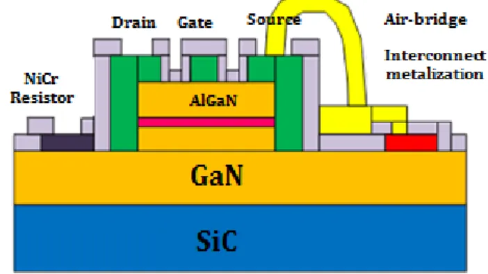
The heterostructure of the active devices is grown using metal organic chemical vapor deposition (MOCVD) on 2-inch semi-insulating SiC substrates due to very high thermal conductivity of SiC [5,8]. Fabrication process consists of mesa etching to isolate the active devices, followed by formation of Ti/Al/Ni/Au (120 Å /1200 Å /350 Å /650 Å) ohmic contacts for drain and source contacts. Gates with a gate length of 0.25 µm are written by using electron beam lithography. NiCr thin film resistors are evaporated in the e-beam evaporator with a sheet resistance of 20Ω/sq. 300 nm SiN was deposited for passivation by using plasma-enhanced chemical vapor deposition (PECVD). Last step is the forming of air-bridges and interconnect metallization. Cross sectional view of the general MMIC process is shown in Fig. 1.
Fig. 1: Cross sectional view of AlGaN/GaN MMIC process
III. DEVICE PERFORMANCE
The 6x75 µm AlGaN/GaN HEMT active device was characterized by using DC-IV, small signal and load-pull measurements. As seen in Fig. 2, the active device cell has a 1.1 A/mm drain current density at Vgs=+1V and 310 mS/mm maximum transconductance. Ft and fmax values were measured as 35 GHz and 49 GHz respectively.
978-2-87487-035-4 © 2014 EuMA 6 -9 Oct 2014, Rome, Italy Proceedings of the 44th European Microwave Conference
Fig. 2: DC-IV and Gm measurement results for 6x75 µm AlGaN/GaN HEMT The 4x75 µm transistor cell had also 1.1A/mm current density at Vgs=+1V and 323 mS/mm transconductance value. 41 GHz ft and 56 GHz fmax values were obtained. This technology has a breakdown voltage (Vbr) of 40V.
After DC and RF characterization, load pull measurements were performed at Vds=15V and Ids = 80 mA for 6x75 µm and Ids= 70 mA for 4x75 µm transistors in order to get the optimum source and load impedance values under non-linear operation for getting the highest output power. TABLE I shows the optimum source and load impedance values for 6x75 µm and 4x75 µm GaN HEMT transistors.
TABLE I: OPTIMUM SOURCE AND LOAD IMPEDANCES OF THE TRANSISTOR CELLS
Transistor Frequency Z-source Z-load 6x75 µm 20.2 GHz 16.3+j*10.4 24.7+j*32.3 20.7 GHz 15.9+j*10.4 23.5+ j*30 21.2 GHz 14.6+j* 12.6 23.2+ j*28.5 4x75 µm 20.2 GHz 10.7+j*14 24.5+ j*46.7 20.7 GHz 11.6+j*13.6 25.7+j*43.2 21.2 GHz 11.7+j*13.9 25.6+j*38.5 According to optimum load impedances given in TABLE I, 6x75 µm transistor cell is delivered a 29.0 dBm output power with a %38 PAE on average at desired frequency range.
IV. CIRCUIT DESIGN
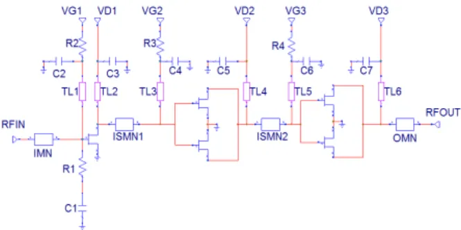
The amplifier is composed of three stages. In order to increase the output power two 6x75 µm transistor cells were used in parallel configuration in power stage. Two 4x75 µm transistors were used in parallel configuration in inter-stage in order to maintain the amplifier linearity by sacrificing the overall PAE. Single 4x75 µm transistor was used in first stage to satisfy the small signal gain requirement of the MMIC amplifier. Overall schematic of the MMIC amplifier can be seen in Fig. 3.
In the first stage, unconditional stability is obtained by using a shunt R-C network consists of R1 and C1 elements.
Fig. 3: Overall schematic of the designed GaN MMIC amplifier
This network also helps the gain flatness of the overall amplifier. For inter-stage and power stage unconditional stability was satisfied by using 50 ohm resistors in the gate bias networks which are R3 and R4 elements in Fig. 3. R2 resistor was also used to guarantee the unconditional stability condition for the first stage. All the gate and drain bias networks which are TL1 to TL6 at the schematic were designed as high impedance λ/4 transmission lines in CPW technology in order to maintain isolation between DC and RF signals. This high impedance bias lines also help the unconditional stability of the overall system and increases overall bandwidth of the amplifier. After realizing the stabilization and bias networks, output matching network of the power stage was designed according to measured optimum load impedances for maximum power transfer. ISMN1 and ISMN2 are the inter-stage matching networks between first to inter – stage and inter-stage to power stages respectively. As a rule of thumb in power amplifier design flow, the output/power stage should always go to compression before the previous stages of the amplifier. By keeping in mind of that rule, these networks (ISMN1 and ISMN2) were designed in order to deliver maximum power from previous amplifier stage to next stage with minimum signal loss and minimum compression according to measured impedance values. All the passive elements used in stabilization, bias networks and matching networks are realized by using Advanced Design System (ADS) Momentum. Simulation results will be presented at next section with measurement results of the GaN MMIC power amplifier.
V. CIRCUIT PERFORMANCE
Fig. 4 shows the photograph of the fabricated GaN MMIC CPW amplifier. The chip dimensions are 5.4 mm x 1.6mm.
Fig. 4: Photograph of the fabricated GaN MMIC amplifier
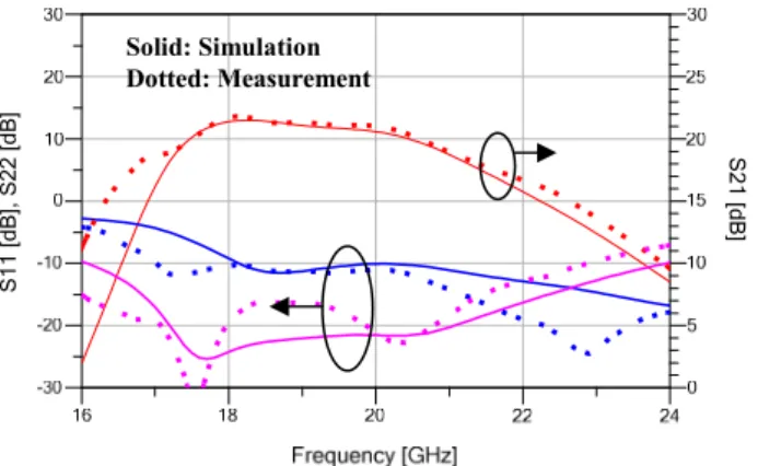
The fabricated MMIC power amplifier was first characterized by small signal s-parameter measurements at a drain voltage of 15 V and total quiescent current of 370 mA. Fig. 5 shows the comparison between small signal simulation (solid) and measurement (dotted) results of the 3-stage GaN MMIC power amplifier. The measurement results were quite promising and showed very good agreement with simulation results. The power amplifier has a 3 dB bandwidth between 17.2 – 21.5 GHz with higher than 17.5 dB small signal gain considering measurement results. Input return loss is lower than -10 dB and output return loss is lower than -16 dB for whole bandwidth. For desired frequency range, 20.2-21.2 GHz, amplifier has small signal gain of higher than 18 dB with maximum of 20.8 dB at 20.2 GHz. The CPW MMIC amplifier is unconditionally stable for whole frequency range.
Fig. 5 : Measured (dotted) and simulated (solid) S-parameters at Vds=15V and total quiescent current of 370 mA.
The band of the amplifier seems more shifted to 18-20 GHz according to both simulation and measurement results. It is mainly caused by the transistors in this technology. Their maximum gain slope has a characteristic of sharp decrease after 20 GHz which is often proportional to the ft values of the transistors.
Fig. 6 shows the large signal measurement (solid) versus simulation (dashed) results of the designed amplifier at Vds=15V with respect to output power. According to measurement results of the amplifier, over 31 dBm at 3 dB gain compression and over 22% of PAE was achieved. The results are quite similar to simulation results as seen from Fig. 6. The overall PAE is lower because of the parallel transistor combination of the inter-gain stage as explained in previous section.
Fig. 6 : Large Signal Measurement Results of the amplifier at Vds=15 V
VI. ENVIRONMENTAL LIFETIME TESTS
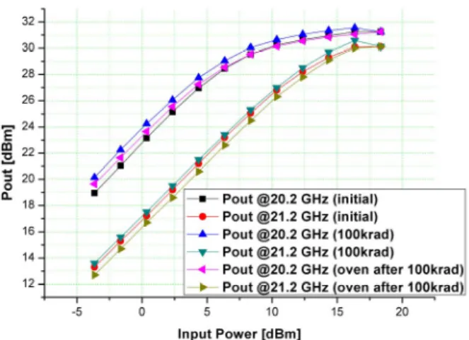
Lastly, accelerated radiation hardness tests were performed in order to predict the radiation lifetime of the amplifier. Accelerated radiation test standards are prepared by European Space Agency (ESA) and clearly stated in [4]. Tests were done at Turkish Atomic Energy Authority (TAEK). For the tests 24 MMIC amplifier samples are selected. All the samples were taken from same fabrication lot. For radiation dose rate window 33 krad was chosen and a total of 100 krad radiation doses was applied 3 times by exposing 33 krad each. ESA states that the time interval from the completion of an exposure to the start of the next exposure shall be maximum of 2 hours. While the tests performed all amplifiers were DC biased but no RF signal was applied. After each exposure all the samples were measured in small signal and large signal conditions. After finishing the radiation tests, all the samples were left under DC bias for 24-hour period at room temperature. After 24-hours duration, all the samples were put into the 90 oC oven with 8 newly prepared amplifier samples (no radiation was applied to those samples), a total of 32 amplifier samples for one week. During that week DC bias was applied to all the amplifiers. Fig. 7 shows the large signal measurement results of one of the 100 krad radiation applied amplifier (before radiation, after radiation and after 1 week oven tests). After the radiation exposure there was no change in the output power. However, after 1-week of oven test nearly 0.5 dB decrease in the output power of the amplifier was observed as seen in Fig. 7. Fig. 8 shows the large signal measurement results of one of the non-exposed amplifier (before 1 week oven, after 1 week oven tests). It was also observed about 0.5 dB decrease in the output power.
S21 [ dB] S 11 [d B ], S 22 [d B ] Solid: Simulation Dotted: Measurement 1494
Fig. 7: Large signal measurement results of one of the 100 krad radiation applied amplifier (before radiation, after radiation and after 1 week oven tests)
Fig. 8: Large signal measurement results of one of the non-exposed amplifier (before 1 week oven, after 1 week oven tests)
As a result, the environment temperature is affecting the amplifier performance and life time. Temperature is a more dominant effect when compared to radiation in space as expected. The radiation effect on GaN material is discussed in [7] and it is stated that radiation environment has no effect on GaN amplifier RF and DC performances.
VII. CONCLUSION
Using a 0.25 µm GaN HEMT technology, a K-band high power GaN HEMT CPW MMIC amplifier has been designed and fabricated. Over 19 dB small signal gain was measured in 20.2-21.2 GHz frequency band. The output power of the amplifier is higher than 31 dBm with over 20% PAE for desired band. Measured performances of the realized MMIC amplifier are in quite good agreement with the electromagnetic simulation results. Lastly, detailed radiation hardness tests were performed for 24 amplifier samples from same fabrication lot and results were presented. Initial
radiation hardness tests indicate a promising stability of the technology in space.
For the frequency band of interest (K-band) microstrip technology with via hole connection to ground is preferred over the traditional CPW technology (no via hole like grounded CPW). Because via hole connection to ground increases the thermal performance of the circuit which often results an increase at output power and overall PAE. On the other hand, traditional CPW technology used in our work has some limitations with respect to thermal performance although SiC has very good thermal properties compared to various materials discussed in [5,8]. Lack of good thermal performance compared to microstrip technology is often limits the output power levels which also directly affects the PAE.
ACKNOWLEDGEMENTS
This work is supported by the projects HAMIT, DPT-FOTON, NATO-SET-193 and TUBITAK under Project Nos., 113E331, 109A015, 109E301. One of the authors (E.O.) also acknowledges partial support from the Turkish Academy of Sciences.
The authors would like to acknowledge G. Orkun Arican, Sinan Osmanoglu, Gokhan Kurt and Yildirim Durmus for their valuable supports. O. Cengiz would like to thank to Ozgur Kelekci for fruitful discussions.
REFERENCES
[1] D. Marcon, J. Viaene, F. Vanaverbeke, X. Kang, S. Lenci, S. Stoffels, R. Venegas, P. Srivastava and S. Decoutere, "GAN-on-Si HEMTs for 50V RF Applications," Microwave Integrated Circuits Conference
(EuMIC), 2012 7th European , vol., no., pp.325 - 328, 29-30 Oct. 2012
[2] Friesicke, C.; Kuhn, J.; Bruckner, P.; Quay, R.; Jacob, A.F., "An efficient AlGaN/GaN HEMT power amplifier MMIC at K-Band," Microwave Integrated Circuits Conference (EuMIC), 2012 7th
European , vol., no., pp.131,134, 29-30 Oct. 2012
[3] P. Khan,L. Epp, and A. Silva “Ka-Band Wideband-Gap Solid-State Power Amplifier: General Architecture Considerations” The Interplanetary Network Progress Report, vol. 42-162, p. 1-19, August 2005
[4] European Space Agency (ESA) “TOTAL DOSE STEADY-STATE IRRADIATION TEST METHOD” ESCC Basic Specification No. 22900
[5] E. Reese, D. Allen, C. Lee, and T. Nguyen, “Wideband power amplifier MMICs utilizing GaN on SiC,” 2010 IEEE MTT-S International Microwave Symposium Digest, pp. 1230 – 1233, June 2002 .
[6] O. Cengiz, O. Kelekci, G.O. Arıcan, E. Ozbay, O. Palamutcuogulları “Design of High Power S-Band GaN MMIC Power Amplifiers for WiMAX Applications” General Assembly and Scientific Symposium,
2011 XXXth URSI, p.1-4, 13-20 Aug. 2011
[7] R. N. Simons and T. R. Oldham “Total Dose Test Report for GaN X-Band Amplifier” NASA Test Report, (2007).
[8] Mishra, Umesh K.; Shen, L.; Kazior, T.E.; Yi-Feng Wu, "GaN-Based RF Power Devices and Amplifiers," Proceedings of the IEEE , vol.96, no.2, pp.287,305, Feb. 2008