S-BAND GAN BASED LOW NOISE MMIC
AMPLIFIER DESIGN AND
CHARACTERIZATION
a thesis submitted to
the graduate school of engineering and science
of bilkent university
in partial fulfillment of the requirements for
the degree of
master of science
in
electrical and electronics engineering
By
Muhittin Ta¸scı
February 2019
S-BAND GAN BASED LOW NOISE MMIC AMPLIFIER DESIGN AND CHARACTERIZATION
By Muhittin Ta¸scı February 2019
We certify that we have read this thesis and that in our opinion it is fully adequate, in scope and in quality, as a thesis for the degree of Master of Science.
Ekmel ¨Ozbay(Advisor)
Vakur B. Ert¨urk
Sefer B. Li¸sesivdin
Approved for the Graduate School of Engineering and Science:
Ezhan Kara¸san
ABSTRACT
S-BAND GAN BASED LOW NOISE MMIC AMPLIFIER
DESIGN AND CHARACTERIZATION
Muhittin Ta¸scı
M.S. in Electrical and Electronics Engineering Advisor: Ekmel ¨Ozbay
February 2019
Low Noise Amplifiers (LNA) are widely preferred components in receiver frontend modules. The received signal level is generally very low and amplifying it without adding too much noise is very crucial in communication systems.
In this thesis study design, fabrication and test of three Gallium Nitride (GaN) High Electron Mobility Transistor (HEMT) based Monolithic Microwave Circuit (MMIC) LNAs are presented. Inductive source feedback topology is used to obtain both better input return loss and noise figure. All three designs achieve higher than 20 dB gain, better than 10 dB input return loss and their noise figure values are 2 dB, 1.5 dB and 1 dB in S-band. High resistive gate biasing is utilized at third design to increase input power handling. Size reduction is very important in MMIC technology. The first design is 3 x 5 mm and the second design is 2 x 3.5 mm, % 46 size reduction is achieved. In GaN technology controlling SiN layer thickness is very problematic and this fabrication step affects capacitor values. The second and third LNA designs presented in this research, matching circuitries and implicitly overall characteristics are not influenced too much by a change of capacitor values. Targeted bandwidth is 2.7-3.5 GHz, achieved frequency range is 1.5 GHz (from 2.5 GHz to 4 GHz). The three LNA designs have 28.1 dBm, 33.4 dBm, and 35.9 dBm output third-order intercept point respectively. Output powers at 1-dB compression points are 18.2 dBm, 23.4 dBm and 25.9 dBm. For all three LNA designs, group delay is less than 0.3 nanoseconds.
Keywords: Low noise amplifier, AlGaN/GaN HEMT, GaN MMIC, T-gate, inter-modulation distortion.
¨
OZET
S-BANT GAN TABANLI D ¨
US
¸ ¨
UK G ¨
UR ¨
ULT ¨
UL ¨
U
Y ¨
UKSELTEC
¸ TASARIMI VE KARAKTER˙IZASYONU
Muhittin Ta¸scı
Elektrik Elektronik M¨uhendisli˘gi, Y¨uksek Lisans Tez Danı¸smanı: Ekmel ¨Ozbay
S¸ubat 2019
D¨u¸s¨uk G¨ur¨ult¨ul¨u Y¨ukselte¸cler (LNA), alıcı ¨on u¸c mod¨ullerinde yaygın olarak tercih edilen bile¸senlerdir. Alınan sinyal seviyesi genellikle ¸cok d¨u¸s¨ukt¨ur ve ¸cok fazla g¨ur¨ult¨u eklemeden y¨ukseltilmesi, ileti¸sim sistemlerinde ¸cok ¨onemlidir.
Bu tez ¸calı¸smasında, ¨u¸c Galyum Nitr¨ur (GaN) Y¨uksek Elektronlu Mobilite Transist¨or¨u (HEMT) bazlı Monolitik Mikrodalga Devresi (MMIC) LNA’larının tasarımı, ¨uretimi ve testi yapılmı¸stır. End¨uktif kaynak geri bildirim topolojisi, hem daha iyi girdi geri d¨on¨u¸s kaybı hem de g¨ur¨ult¨u fig¨ur¨u elde etmek i¸cin kul-lanılmı¸stır. Her ¨u¸c tasarım da 20 dB’den y¨uksek kazan¸c, 10 dB’den daha iyi giri¸s geri d¨on¨u¸s kaybı verir ve g¨ur¨ult¨u fig¨ur¨u de˘gerleri S-bandında 2 dB, 1.5 dB ve 1 dB’dir. Giri¸s g¨uc¨u dayanımını artırmak i¸cin ¨u¸c¨unc¨u tasarımda y¨uksek diren¸cli ge¸cit beslemesi kullanılmı¸stır. MMIC teknolojisinde boyut k¨u¸c¨ultme ¸cok ¨onemlidir. ˙Ilk tasarım 3 x 5 mm ve ikinci tasarım 2 x 3,5 mm’dir, % 46 boyut k¨u¸c¨ultme elde edilmi¸stir. GaN teknolojisinde SiN katman kalınlı˘gının kon-trol edilmesi problemlidir ve bu imalat adımı kapasit¨or de˘gerlerini etkiler. Bu ara¸stırmada sunulan ikinci ve ¨u¸c¨unc¨u LNA tasarımları, uyumlama devreleri ve dolaylı olarak genel ¨ozellikler, kapasit¨or de˘gerlerinin de˘gi¸smesinden ¸cok fazla etk-ilenmemektedir. Hedeflenen bant geni¸sli˘gi 2,7-3,5 GHz, ula¸sılan frekans aralı˘gı 1,5 GHz’dir (2,5 GHz - 4 GHz). ¨U¸c LNA tasarımında sırasıyla 28.1 dBm, 33.4 dBm ve 35.9 dBm ¸cıkı¸s ¨u¸c¨unc¨u dereceden kesme noktası vardır. 1 dB sıkı¸stırma nokta-larındaki ¸cıkı¸s g¨u¸cleri 18,2 dBm, 23,4 dBm ve 25,9 dBm’dir. ¨U¸c LNA tasarımının t¨um¨u i¸cin grup gecikmesi 0,3 nanosaniyeden azdır.
Anahtar s¨ozc¨ukler : D¨u¸s¨uk g¨ur¨ult¨ul¨u y¨ukselte¸c, AlGaN/GaN HEMT, GaN MMIC, T-Kapı, ˙Intermodulasyon distorsiyonu.
Acknowledgement
I would like to express my sincere gratitude to my supervisor Prof. Dr. Ekmel ¨
Ozbay, for his valuable support and encouragement throughout this thesis study. It is an honour to work at various advanced technology projects under supervision of him. I am also thankful to Prof. Dr. Vakur B. Ert¨urk and Prof. Dr. Sefer B. Li¸sesivdin for being part of my graduate committee.
I owe my deepest thanks to RF group leader Dr. ¨Ozlem Apaydın S¸en who gave numerous and priceless comments and advices throughout this study. Without her encouragement this project and thesis study would not be finished. I always felt lucky when I was working with her. Halil Akcalı was like my brother in NANOTAM. Research, design and measurement were more enjoyable with him.
I am thankful to my colleagues from NANOTAM and ASELSAN B˙ILKENT Micronano: Ula¸s ¨Ozipek, Batuhan S¨utba¸s, Yi˘git Ba¸ser, Erdem Aras, Muhammet Kavu¸stu, Ahmet Toprak, Dr. Bayram B¨ut¨un, Do˘gan Yılmaz, Yıldırım Durmu¸s, and G¨okhan Kurt (in no particular order).
I am also thankful to my friends Faruk Uyar, Bensigu ¨Ozbay, Mustafa G¨ul, Mustafa Tonbul, and Ekrem Sidat for their support. Spatial thanks to my mus-tachioed brother Zafer Tan¸c.
This project and thesis study is aimed to provide MMICs for the use of ASEL-SAN Inc. and this work is funded by Turkish Scientific and Technological Re-search Council (TUB˙ITAK) and Presidency of Defence Industries (SSB) as an Industrial Thesis (SAN-TEZ) project.
Finally, my special thanks belong to my family, my father Sebahattin, my mother G¨uler, and my sisters Ay¸se and Hacer. I dedicate my thesis work to my nephews Ahmet, Melis Ada, and Hakan.
Contents
1 Introduction 1
1.1 Low Noise Amplifier Fundamentals . . . 2
2 HEMT and MMIC Fabrication 9 2.1 Fabrication Steps . . . 11
3 HEMT Characterization 17 3.1 DC Characterization . . . 18
3.2 RF Characterization . . . 22
4 MMIC Design and Simulation 25 4.1 LNA Design Procedure . . . 25
4.1.1 Requirements . . . 27
4.1.2 HEMT Selection . . . 27
CONTENTS vii
4.1.4 HEMT RF and NF Characteristics . . . 31
4.1.5 Methodology . . . 33
4.2 First LNA Design . . . 35
4.3 Second LNA Design . . . 38
4.3.1 Schematic . . . 39
4.3.2 Realization . . . 40
4.3.3 Layout . . . 45
4.3.4 Simulation Results . . . 46
4.3.5 Effect of SiN Thickness Variance . . . 48
4.4 Third LNA Design . . . 49
5 Measurement Setups and Results 51 5.1 Measurement Setups . . . 51
5.1.1 S-Parameter and Group Delay Measurement Setup . . . . 51
5.1.2 Noise Figure Measurement Setup . . . 52
5.1.3 1 dB Compression Point Measurement Setup . . . 54
5.1.4 Third Order Intercept Point Measurement Setup . . . 55
5.2 Measurement Results . . . 57
5.2.1 Measurement Results of the First LNA Design . . . 57
CONTENTS viii
5.2.3 Measurement Results of the Third LNA Design . . . 64 5.3 Simulation and Measurement Comparison . . . 66
List of Figures
1.1 3D representation of NF . . . 3
1.2 Single stage LNA topology . . . 5
1.3 Two stage LNA . . . 6
1.4 Cascaded LNA system . . . 7
2.1 Substrate . . . 10
2.2 Cross sectional view of HEMT . . . 10
2.3 HEMT and RLC circuitry . . . 11
2.4 a) Photomask of the ohmic, mesa, and gate layers b) Cross sec-tional view of T-Gate, c) SEM image of the gate. . . 13
2.5 Photomask of the resistor, thin metal, and opening layers . . . 14
2.6 a) Photomask of the air bridge layer, b) SEM image of air bridge 15 2.7 a) SEM image of an inductor before bridge post cleaning, b) SEM image of an HEMT . . . 16
LIST OF FIGURES x
3.2 a) TLM pattern, b) TLM measurement results . . . 19
3.3 Resistor pattern . . . 19
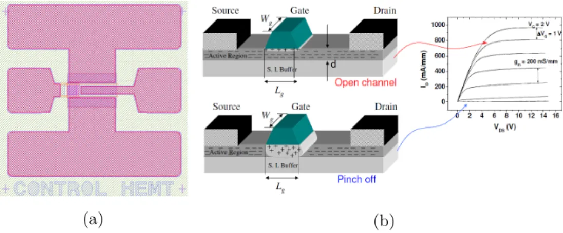
3.4 a) Control HEMT, b) I-V characteristic . . . 20
3.5 DC measurements of a control HEMT a) Id-Vd , b) gm , c) Vbr . . 21
3.6 DC measurements of source degenerated HEMT a)Id-Vd , b) gm , c) Vbr . . . 22
3.7 ft and fmax measurement . . . 23
3.8 Different HEMT Layout Designs . . . 23
3.9 S-parameter measurements of the different HEMT designs a) S11, b) S22, c) S21 . . . 24
4.1 LNA design procedure . . . 26
4.2 Small signal model of HEMT . . . 29
4.3 12-Term equivalent circuit modeling schematic . . . 29
4.4 12-Term equivalent circuit modeling results and measurement . . 30
4.5 S parameter curves of the HEMT . . . 31
4.6 NF of the HEMT . . . 31
4.7 Constant gain and NF circles . . . 32
4.8 Input matching (Lg), SD HEMT and RLC transformed version of circuitry . . . 34
LIST OF FIGURES xi
4.10 Layout of the first LNA design . . . 36
4.11 Photograph of the first LNA design . . . 36
4.12 Simulation results of the first LNA design . . . 37
4.13 Simplified schematic of the second LNA design . . . 39
4.14 Schematic of the second LNA design . . . 40
4.15 a) IMN, b) ISMN, c) OMN. . . 41
4.16 Combining separate EM simulations . . . 41
4.17 a) Stability analysis of the first stage, b) Stability analysis of the second stage. . . 42
4.18 EM simulation of two stage LNA design . . . 43
4.19 Zoomed EM simulation . . . 43
4.20 Mesh diagram of EM simulation of two stage LNA design . . . 44
4.21 a) Two stage LNA design simulation with EM simulation data, b) Stability analysis of two stage LNA design . . . 45
4.22 Layout of the second LNA design . . . 45
4.23 Photograph of the second LNA design . . . 46
4.24 a) |S11| and |S22| simulation results of the second LNA design, b) |S21| simulation curves of the second LNA design, c) NF simulation curve of the second LNA design . . . 47
4.25 SiN thickness variance simulation of the second LNA design . . . 48 4.26 SiN thickness variance simulation results of the second LNA design 49
LIST OF FIGURES xii
4.27 Simplified schematic of the third LNA design . . . 50
4.28 Layout of the third LNA design . . . 50
5.1 S-parameter and group delay measurement setup . . . 52
5.2 NF measurement setup . . . 53
5.3 Photography of NF measurement setup . . . 53
5.4 1 dB compression point measurement setup . . . 54
5.5 Third order intercept point measurement setup 1 . . . 56
5.6 Third order intercept point measurement setup 2 . . . 57
5.7 NF and S-parameter measurements of the first LNA . . . 58
5.8 TOI measurement result of the first LNA design via spectrum an-alyzer . . . 59
5.9 TOI measurement result of the first LNA design via ZVA40 VNA 60 5.10 a) Input Power vs Gain, b) Input Power vs Output Power . . . . 61
5.11 NF and S-parameter measurements of the second LNA . . . 62
5.12 Group delay measurement result of the second LNA design . . . . 63
5.13 TOI measurement result of the second LNA design via spectrum analyzer . . . 63
5.14 NF and S-parameter measurements of the third LNA . . . 64
5.15 TOI measurement result of the third LNA design via spectrum analyzer . . . 65
LIST OF FIGURES xiii
5.16 3rd order and fundamental signal levels vs input power measure-ment result of the third LNA design . . . 65
List of Tables
1.1 Semiconductor Material Parameters [1] . . . 1
4.1 Requirements . . . 27 4.2 Topology Comparison . . . 33
5.1 Simulation and Measurement Comparison of the LNA Designs . . 66 5.2 Comparison with Literature . . . 67
Chapter 1
Introduction
Gallium nitride (GaN) was deemed an excellent, next generation, semiconductor material because of its properties [1]. GaN has high bandgap, moderate electron mobility, good thermal conductivity and high breakdown voltage. Semiconductor material parameters are shown in Table 1.1. Besides these superior properties for power applications also sub-dB noise figure (NF) values are reported, as well [2]. In addition, robust LNA designs can be achieved by using GaN [3]. Without NF performance degradation, GaN LNA enables high input power handling. Overall system noise figure can be decreased since there is no need for input protection circuitries. [4].
Table 1.1: Semiconductor Material Parameters [1]
Semiconductor Si SiC GaAs GaN
Characteristic Unit
Bandgap eV 1.1 3.25 1.42 3.49
e-mobility at 300◦ K cm2/V s 1,500 700 8,500 1,000–2,000
Saturated Electron Velocity x107cm/s 1 2 1.3 2.5
Critical Breakdown Field MV/cm 0.3 3 0.4 3.3
Thermal Conductivity W/cm◦K 1.5 4.5 0.5 >1.5
In this thesis study, design, fabrication and measurement of three Gallium Nitride (GaN) High Electron Mobility Transistor (HEMT) based Monolithic Mi-crowave Circuit (MMIC) LNAs are presented. Inductive source feedback topology is used to obtain both better input return loss and noise figure. Coplanar waveg-uide technology is utilized in all three LNA designs. Since there is no ground via at this technology, coplanar line is easy to fabricate and it does not require backside process. It has low loss, however fields are more sensitive to signals that come from outside [5]. Signal line requires a ground plane on both side, so total size of the chip increases.
1.1
Low Noise Amplifier Fundamentals
Some important key parameters, which are to be in designing LNAs, should be clarified. The following formulations help us to understand the fundamentals of the LNA design.
NFmin is the minimum noise figure that can be achieved from HEMT Γopt is the optimum source reflection coefficient for achieving NFmin
Yopt is the optimum source admittance (Yopt = gopt + jbopt = 1/Zopt)
Rn is the noise resistance of the HEMT
rn is the normailized noise resistance (rn = Rn / Z0, Z0 = 50 Ω)
ZS is the actual source impedance that is seen by the input of the HEMT
YS is the source admittance (YS = gs + jbs = 1/ZS)
Noise Figure: Equation 1.1 gives the relation between noise figure and rn,
gs, YS, Yopt. rn depends on HEMT design and quality of the fabrication process.
gs and YS depend on input design topology and they can be optimized according
however in addition to that Yopt can be optimized and configured before design
process. In this thesis work, HEMTs that are used in the LNA designs are pre-designed by adding inductors at the source. This topology is termed as source degeneration. Yopt is changed (actually designed) according to input reflection
and noise figure requirements. Source degeneration is utilized for making Yopt
closer to Ys. It does not contribute to overall noise figure, however it diminishes
the amplifier gain.
NF = NFmin + (rn/gs)|YS− Yopt|2 (1.1)
As it can be seen from equation 1.1, minimum noise figure can be achieved by matching the input admittance to Yopt. Any YS value different than Yopt results
in higher noise figure [6]. This equation 1.1 gives NF circles. 3D representation of this phenomenon is shown in Figure 1.1
Figure 1.1: 3D representation of NF
Noise factor expression for cascaded systems is shown in 1.2. This expression clearly shows that noise factor (overall noise figure) is dominated by the NF of
the first stage [5]. Fcascade= F1+ F2− 1 GA1 + F3− 1 GA1GA2 + ... (1.2)
Stability: Stability factor, K, shows the stability condition for passive source and load terminations. If K is higher than 1, for any input and output impedance, device is unconditionally stable. ∆ should be less than 1 for unconditional sta-bility [7]. K = 1 − |S11| 2−|S 22|2+|∆|2 2|S21S12| > 1 (1.3) |∆|= |S11S22− S21S12| < 1 (1.4)
Edwars and Sinsky proposed a single stability definition known as µ factor which is given in equation 1.5. Different than K, larger values of µ factor imply greater device stability. K indicates the stability condition alone, whereas µ factor also gives information about the relative level of the device stability [8].
µ = 1 − |S11|
2
|S22− S11∗ ∆|+|S21S12|
> 1 (1.5)
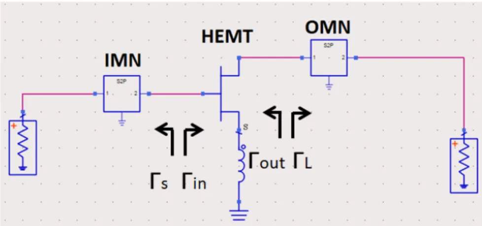
Matching Circuitries: Single stage LNA topology is shown in Figure 1.2. IMN and OMN refer to the input matching network and output matching network, respectively.
Figure 1.2: Single stage LNA topology
In order to achieve maximum gain, OMN is needed to transform the load impedance, ZLinto 50 Ω. ZL can be calculated from equation 1.7. Besides, ΓL is
needed to be equal to Γ∗out for maximizing gain. Conjugate matching is important to reduce the mismatch loss [9]. ΓLcan be obtained from equation 1.6 when input
is terminated with ΓS. ΓL= Γ∗out= (S22+ S12S21ΓS 1 − S11ΓS )∗ (1.6) ZL= Z0 1 + ΓL 1 − ΓL (1.7) After maximum gain and minimum mismatch loss are accomplished by means of optimum OMN circuitry, design proceeds with IMN design. In order to achive minimum NF, IMN is needed to transform 50 Ω into the source impedance, ZS,
where ZS is equal to Zopt∗ . Almost no HEMT has Zin value that is equal to Zopt∗ .
Zin can be calculated from equations 1.9 and 1.8 when output is terminated
with ΓL.
Γin = S11+
S12S21ΓL
1 − S22ΓL
Zin = Z0
1 + Γin
1 − Γin
(1.9) Two stage LNA topology is shown in Figure 1.3. ISMN refers to inter-stage matching network. IMN and OMN designs have similar approach that is proceed in single stage LNA design. ISMN design methodology is based on conjugate matching in order to minimize ML.
Figure 1.3: Two stage LNA
ML can be calculated via equation 1.10 and related reflection coefficient can be obtained from equation 1.11. Return loss, RL and Γ relationship is shown in equation 1.12 and RL can be obtained by using equation 1.13. For minimum NF, ΓS should be taken as Γopt.
M L = (1 − |Γin|
2)(1 − |Γ S|2)
|1 − ΓinΓS|2
(1.10) Importance of the mismatch loss: ML directly affects the overall system performance, giving rise to higher NF and lower gain. Cascaded system that is depicted in Figure 1.4 can be given as an example. In this system, assume that first stage has prefect input match (ML = 0 dB) and second stage has perfect output match (ML = 0 dB). First stage has 10 dB output return loss, and the second stage has 10 dB input return loss. From this cascaded system gain should not be expected as 48 dB rather than that it should be expected 46.4 dB to 47.2
dB. This gain variation changes according to the line length of the connection, phase, Φ, is the key parameter.
Figure 1.4: Cascaded LNA system
Γ =√1 − M L (1.11) RL = 20 log(|Γ|) (1.12) RL = 10 log(|1 −(1 − |Γin| 2)(1 − |Γ S|2) |1 − ΓinΓS|2 |) (1.13)
Trading output match for improved input match: HEMT has gate to drain capacitance, Cgd, indicating that the device is bilateral. Therefore, input
and output are not completely isolated. Any change in output matching affects input matching, and vice versa. Therefore, a certain value of ΓL improves Zin.
ΓL can be obtained by solving equation 1.8 in terms of Γin. Substitute Γin to
Γ∗opt, then perfect input RL and noise match with an acceptable output RL can be obtained [10].
ΓL=
Γin− S11
S12S21− S11S22+ S22Γin
Linearity: Linearity defines the input and output characteristics of an amplifier. In linear region of amplification, gain is constant and independent of input power level. Output P1dB is defined as the output power level at which the actual gain deviates from the small signal gain by 1 dB. P1dB is a measure of the power capacity, and it defines the linear region of the amplifier. The extrapolation point where the curve of the third harmonic power crosses that of the fundamental one is called third harmonic intercept, TOI, point. TOI is measure of the non-linearity of the amplifier. At high input power conditions, device under test, DUT, draws higher current and reaches its maximum limit around which amplifier behaves non linear and output power saturates. Non linearity causes intermodulation distortion [8, 11].
Chapter 2
HEMT and MMIC Fabrication
In this section, fabrication steps of AlGaN/GaN HEMT and MMIC will be inves-tigated. In order to show the procedure of fabrication of an MMIC, mask layers and SEM images of devices will be used. Each step has separate photomask and these photomasks are used during the photolithography process. The mask lay-ers are designed at Advanced Design System (ADS) software tool and then they imported to KLayout program to have a better representation of them. In the fabrication step sections fabrication details, etching, deposition, photolithogra-phy, and other important key features will be given. The main objective of this section is to present the fabrication procedure of RF circuitry.
Bottom-up approach is utilized, therefore materials such as Ti, Ni, Au, SiN are assembled on the bulk substrate. The substrate can be sapphire, SiC or any bulk material that is preferred according to application, budget, and capability of fabrication. Substrate that is used in each of the LNA designs is shown in Figure 2.1. Met1 represents thin metal layer, resistor1 indicates resistor layer and int2 stands for interconnect metal layer. Opening2 provides a connection between thin metal layer to interconnect metal layer and resistor layer to interconnect metal layer.
Figure 2.1: Substrate
Figure 2.2 shows a cross sectional view of HEMT.
Figure 2.2: Cross sectional view of HEMT
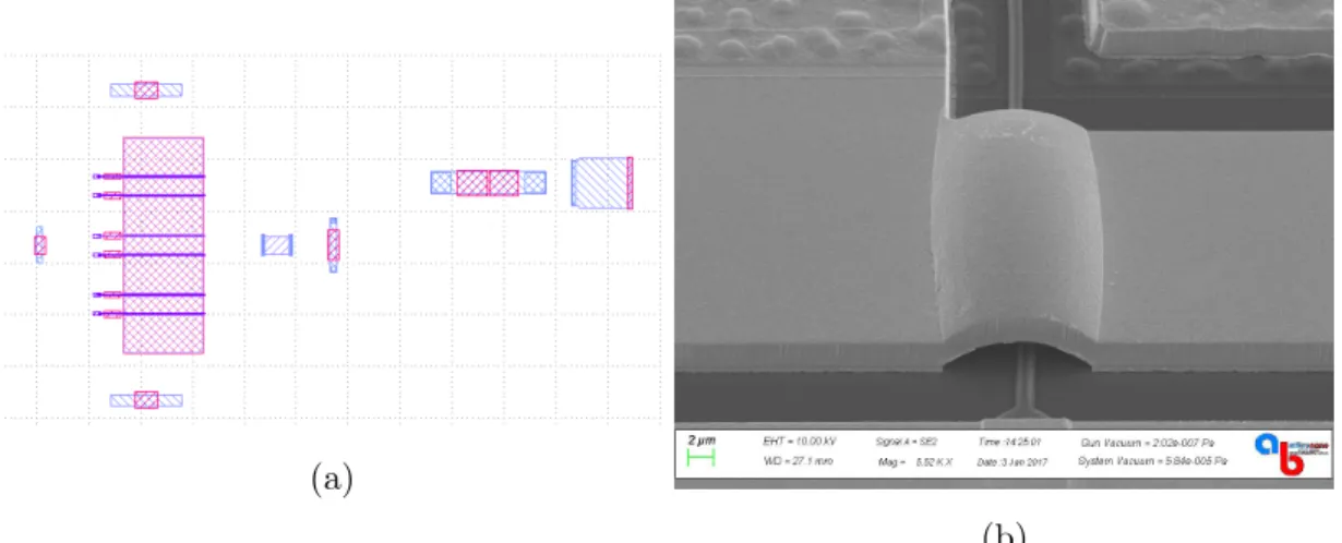
Figure 2.3 shows us a layout of a HEMT and RLC circuitry, for the sake of simplicity and in order to relay information more accurately I draw simplistic layout rather than giving complicated low noise amplifier. This layout has active elements High Electron Mobility Transistor (HEMT) and also lumped elements a resistor, an inductor, a capacitor.
Figure 2.3: HEMT and RLC circuitry
2.1
Fabrication Steps
Cleaning: Wafer should be agitated with Acetone in the ultra-sonic bath. Wafer should be dried via nitrogen gun. Wafer surface should be checked via optic microscope whether there is contamination or not. If there is a contamination, wafer will be put into AZ100 and water (1:1) solution. After that wafer should be rinsed via de-ionized water. If there is any contamination, then these steps should be repeated again and again until wafer surface is become clean.
Ohmic: AZ5214E photoresist will be coated on the surface of the wafer, the spinner rotation speed should be adjusted to achieve the desired thickness. Softbake will be done in order to increase the resist density on a hot plate. After proximity alignment, expose pattern on the wafer. Hardbake will be done on a hot plate. Using AZ400K / Di-water (1:4) solution development will be done in
1 minute. After that pattern will be checked via an optical microscope. If there is no dirt on the wafer, the asher process will be done. With the help of plasma ashing process, the photoresist will be removed. Using E-beam evaporator Ti, Al, Ni, and Au will be coated, the thickness of each metal is very important since it affects the overall performance of the transistor. Therefore, current, speed, temperature, and pressure values of E-beam evaporator should be controlled. After, coating procedure wafer will be lifted off. Metal layers should be checked whether there is any problem or not. If there is no physical problem wafer will be agitated with acetone. After the cleaning process annealing will be done by using RTP(Rapid Thermal Processing) system. Wafer will be annealed and after annealing process distance between the source and drain should be checked.
Mesa: Cleaning procedure should be done before starting the mesa fabrica-tion step. AZ5214E photoresist will be coated on the surface of the wafer, the spinner rotation speed should be adjusted to achieve the desired thickness. Soft-bake will be done in order to increase the resist density on a hot plate. Edge bead should be cleaned by using swab and acetone. After proximity alignment at mask aligner, wafer pattering can be done. This alignment and exposure step should be done in hard contact mode. Using AZ400K / Di-water (1:4) solution development will be done. In order to etch the mesa pattern, inductively coupled plasma – reactive ion etching (ICP-RIE) machine will be used. After etching Al2O3 will be
coated by using electron beam evaporator, the thickness will be adjusted to 200 ˚
A. After this process wafer should be agitated and cleaning procedure should be done. By using Dektak profilometer mesa pattern depth should be measured.
Gate: Wafer cleanness should be checked before starting gate lithography and metallization process. PMMA e-beam resist will be coated on the surface of the wafer, the spinner rotation speed should be adjusted to achieve the desired thickness. Wafer will be heated on a hot plate. After that wafer will be placed in an electron beam lithography machine. Proper alignment will be made via alignment marks and conditioning of the EBL machine will be done. Electron beam exposure changes e beam resist and during the development process these patterns will be removed. Patterns will be checked via a scanning electron mi-croscope. If there is no dirt on the gate pattern, Ni and Au metals will be coated
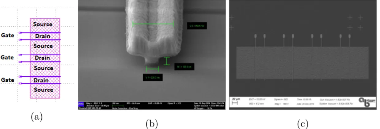
respectively. Ni and Au coating process current, speed, and temperature are dif-ferent. 50 nm Ni and 300 nm Au will be coated at the end of this process. After coating process wafer will be lifted off via acetone, it will take almost one day. After liftoff wafer will be agitated, and cleaned. Morphological properties of the gate will be checked via SEM. Photomask of the ohmic, mesa and gate layers are shown in Figure 2.4a. Cross sectional view of T-Gate is depicted in Figure 2.4b. SEM image of the gate is shown in Figure 2.4c.
(a)
(b) (c)
Figure 2.4: a) Photomask of the ohmic, mesa, and gate layers b) Cross sectional view of T-Gate, c) SEM image of the gate.
Resistor: As usual this fabrication step also starts with wafer cleaning, after the cleaning process is done AZ5214E photoresist will be coated on the surface of the wafer. Softbake will be done in order to increase the resist density on a hot plate. After the proximity alignment, pattern will be exposed on the wafer, this step will be done via soft contact mode. Using AZ400K / Di-water (1:4) solution development will be done. Using E beam evaporator NiCr will be coated. In order to achieve the desired sheet resistance, thickness will be adjusted to 850 ˚A. For this process etch back will be utilized in order to etch unwanted materials. In this fabrication step, TLM measurement is made to decide whether production will continue or not. TLM measurement will be explained in the characterization section.
Thin Metal: AZ5214 photoresist will be coated. Softbake will be done. Using the following photomask which is shown in Figure 2.5 photolithography will
be done. After the alignment, exposure rate will be adjusted and wafer will be patterned. Using AZ400K / Di-water (1:4) solution wafer will be developed. After development via E-Beam Evaporator Ti coating will be done, 50 nm thickness will be achieved. Again using E-Beam Evaporator Au Coating will be done, 350 nm thickness will be achieved. By lift off this fabrication step is finalized.
Dielectric Coating: Using PECVD system Si3N4 will be coated to the
whole surface. Si3N4 thickness will be 200 nm. By changing PECVD
condi-tioning parameters different thickness values will be acvhieved, but this variance will change whole structure for some elements like capacitor values. Therefore, achieved thickness and homogeneity of this layer are important, so thickness should be checked via ellipsometer.
Figure 2.5: Photomask of the resistor, thin metal, and opening layers
Opening: Opening holes enable us to connect cond to cond2 and cond2 to resi layers. AZ5214 photoresist will be coated and softbake will be done. Using AZ400K / Di-water (1:4) solution development will be done. Using Reactive Ion Etching method unwanted areas will be etched.
Air Bridge: This structure enables us to equate the potentials of ground planes. Our device is constructed as a coplanar waveguide so that potential equivalence between two grounds should be ensured. S1828 photoresist will be coated. Softbake will be done. Development will be done via AZ326. Photomask of the air bridge layer is shown in Figure 2.6a and SEM image of the air bridge is shown in Figure 2.6b.
(a)
(b)
Figure 2.6: a) Photomask of the air bridge layer, b) SEM image of air bridge
Interconnect Metal: AZ2070 photoresist will be coated. Softbake will be done. After exposure, hardbake will be done. Then using AZ826 development will be done. By using E-Beam Evaporator system Ti will be coated for 250 nm thickness. After that 1 um Au will be coated. Then lift off will take place in acetone bath.
Bridge Post Cleaning: Intentionally bridge photoresist S1828 is left be-tween thin metal and interconnect metal. This photoresist is used in order not to have a short circuit between signal and ground. After interconnect metalization, this photoresist is removed via AZ100 remover. After this cleaning process, air bridge fabrication step is done. Figure 2.7a is an SEM image of an inductor before bridge post cleaning photoresist (dark material) between two metal can be seen. Figure 2.7b depicts the image of an HEMT.
(a) (b)
Figure 2.7: a) SEM image of an inductor before bridge post cleaning, b) SEM image of an HEMT
Chapter 3
HEMT Characterization
In this section, DC, RF, and NF characterization and measurement methods are presented. Making an accurate and reliable measurement is as important as hav-ing a good fabrication and design, thus each and every step is measured even during the fabrication process of the devices. TLM measurement techniques and why it is so important for the fabrication are presented. Resistor pattern is placed in every reticle of the wafer. The need for its characterization in each rectile is explicated as well. Another essential design component is Control HEMT, as a rule of thumb it is placed in every reticle and all of them are characterized in DC measurements. DC measurements of the Control HEMTs IV, gm, and Vbr are explained and measurement results are given. Source degenerated HEMT DC, RF and NF measurements are also presented. Maximum Gain and Stability Fac-tor of the same HEMT in different fabrication are given and results are discussed. Current Gain and Maximum Stable Gain vs Maximum Available Gain measure-ment of a HEMT that is used in one of the low noise amplifier design are given and the importance of these measurements are mentioned. Source degenerated HEMTs which have different inductance values are presented and their s param-eter differences will be investigated. At the end of this section suitable HEMTs for LNA applications will be clarified. All DC characterization measurements are taken with B1500A Semiconductor Device Parameter Analyzer and DC probe station.
3.1
DC Characterization
Figure 3.1: B1500A semiconductor device parameter analyzer
Wafer characterization starts with Transmission Line Method (TLM) measure-ments which are performed after ohmic contact metallization in order to deter-mine the sheet resistance of the ohmic contact layer. Since contact resistance affects the device performance significantly, it should be determined correctly. Fabrication is stopeed if the measured values of contact resistance is too high, since active device characteristics, particularly noise figure, are highly dependent on ohmic layer related resistances. Between each rectangular ohmic contact re-gion, there are specific separations, which are 2 um, 3 um, 5 um, 7 um, 10 um, and 21 um. Typical ohmic contact values are within the range 0.2 to 0.5 Ohm-mm. Sheet resistance should be between 300 to 600 Ohm/square. This sheet resistance can be used in gate biasing at low noise amplifier design. Sheet resistance is a parameter that cannot be easily controlled, therefore it should not be used in matching circuitry.
(a) (b)
Figure 3.2: a) TLM pattern, b) TLM measurement results
Sheet and contact resistances are important parameters and they should be measured before and after each fabrication step. As it is mentioned in Chapter 2, there is a resistor layer in our fabrication steps. Resistor pattern is also measured to understand the quality of the resistor fabrication. As opposed to the sheet resistance, it is easier to control resistor pattern. Typical one square resistor pattern is between 14.5 to 15.5 Ohm. In design and layout simulation steps 15 Ohm/square is taken as an average value.
Figure 3.3: Resistor pattern
Control HEMTs are placed in every wafer and they are measured both during the process and at the end of the fabrication process. Control HEMTs are iden-tical and they indicate the active device characteristics of the fabrication. DC measurements are taken for each Control HEMT.
(a) (b)
Figure 3.4: a) Control HEMT, b) I-V characteristic
During DC measurements there are some key parameters that indicate the DC characteristics of the HEMT, namely transconductance (gm), Idrain vs Vdrain,
knee voltage (Vknee), and breakdown voltage (Vbr). gm of the device decreases as
the negative bias on the gate is increased [12]. gm is an indicator of the HEMT
gain. gm equation is given in 3.1 which shows the input output relationship of
the HEMT. gm value is 44 mS for the measured control HEMT.
gm =
∂Id
∂Vg
(3.1) If, is shown in Figure 3.5a, denoting the current per millimetre of the gate
width [12]. Typical If is 1 A/mm and control HEMT satisfies this value since
it has 2 fingers with 100 µm. Vknee is the minimum drain voltage which is
re-quired for the smooth operation of HEMT. Vknee value is 6 Volts for measured
control HEMT. Vpinch−of f indicates the gate threshold voltage, beyond which
HEMT becomes operational. Vpinch−of f value is -4 Volts for measured control
HEMT. There are several breakdown voltage mechanisms such as: source-drain breakdown (punch-through), gate-drain breakdown (leakage through the Schot-tky diode), vertical breakdown (poor compensation of the buffer layer) [13, 14]. Vbr measurement drain current upper limit is specified as 1 mA, therefore at this
(a) (b)
(c)
Figure 3.5: DC measurements of a control HEMT a) Id-Vd , b) gm , c) Vbr
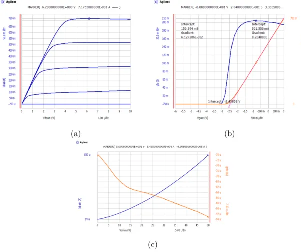
gm is 150 mS, If is 720 mA, Vknee is 5 Volts, Vpinch−of f is -3 Volts, Vbr is higher
than 50 Volts for measured source degenerated HEMT. Id-Vd measurement of
source degenerated HEMT is shown in Figure 3.6a, gm is shown in Figure 3.6b,
(a) (b)
(c)
Figure 3.6: DC measurements of source degenerated HEMT a)Id-Vd , b) gm , c)
Vbr
3.2
RF Characterization
ft is the frequency at which the short-circuit gain is equal to 0 dB. fmax is the
frequency at which maximum available power gain is equal to 0 dB. ft and fmax
values can be calculated from s parameters. As a rule of thumb, ft and fmax
values should be three times higher than the operational frequency. In this study this values are seven times higher than the required frequency.
Figure 3.7: ft and fmax measurement
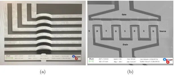
Initial step for the LNA design is the design of a proper HEMT. In order to achieve optimum HEMT structure, empirical design approach is utilized. Several HEMT layouts are designed. Some of them have different inductor values (from 0.2 nH to 1.5 nH) in their sources. Gate finger number is swept from 2 to 10 fingers. Different HEMT layout designs are shown in Figure 3.8.
Figure 3.8: Different HEMT Layout Designs
S-parameter measurement results are shown in Figure 3.9a, Figure 3.9b, and Figure 3.9c.
(a) (b)
(c)
Figure 3.9: S-parameter measurements of the different HEMT designs a) S11, b)
S22, c) S21
Remarks: According to s-parameter measurment results, the source induc-tance value and the HEMT gain is inversely proportional. Higher inducinduc-tance at the source brings Zin value closer to Zopt∗ value. Inductor value is optimized via
emprical design and measurement methodology. Optimum gate finger number and inductance value are chosen according to these measurement results.
Chapter 4
MMIC Design and Simulation
In this section, LNA design procedure, requirement definitions, HEMT selection, HEMT modeling, topology preferences, design, and electromagnetic (EM) simu-lation flow are investigated.
4.1
LNA Design Procedure
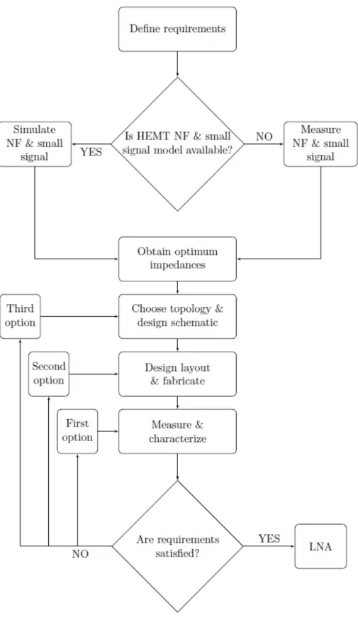
LNA design procedure starts with specifying requirements, continues with selec-tion of the proper HEMT, followed by HEMT modelling. Optimum impedances for NF, gain, input and output return losses should be determined, suitable topol-ogy should be chosen, then schematic and layout design should be tuned and optimized by using Advanced Design System EM simulation software. Finalized layout is then fabricated. After measurement and characterization of the MMIC, LNA design procedure is finished aiming to the fulfillment of the requirements. LNA desing procedure flow diagram is shown in Figure 4.1.
4.1.1
Requirements
In this thesis, it is aimed to design an MMIC low noise amplifier in order to use in S-Band radar applications. Operating frequency band is chosen as 2.7 GHz to 3.5 GHz, target gain in this band is higher than 20 dB, power output at 1 dB compression point is expected to be higher than 20 dBm, output third-order intercept point is targeted as higher than 30 dBm, aimed noise figure value of this amplifier is less than 2 dB, and finally more than 9 dB input and output return losses are expected to be satisfied.
Table 4.1: Requirements Req. Type Req. Value Units
Frequency 2.7 - 3.5 GHz |S21| >20 dB NF <2 dB |S11| & |S22| <-9 dB P1dB >20 dBm TOI >30 dBm
4.1.2
HEMT Selection
After specifying requirements, proper HEMT which is adequate to satisfy all re-quirements with a proper topology should be chosen. In characterization section, RF measurements of source degenerated HEMTs (which have different inductance values at source) are depicted. During HEMT selection procedure following pa-rameters are considered:
Maximum Available Gain Circles Noise Figure Circles
Source and Load Impedances
Gate Length & Gate Width & Gate Shape (T, Γ, I) Drain-Source Separation & Number of Gate Fingers
Remarks: There are several relationships between these parameters; if gate length is decreased, gain (gm) and gate resistance (Rg) increase. Moreover, effect
of gate length on Fmin varies depending on the frequency. In high frequencies, effect of gm is more dominant than the effect of Rg. Rise of gm reduces Fmin,
increase of Rg increases Fmin, therefore, the effect of gate length on Fmin is
limited. Reduction of gate to source and gate to drain separation decreases Fmin, however gate can be shorted out easily during the fabrication process. Thus separation limitation is determined by fabrication capability. Increase in number of gates reduces Fmin , nevertheless it also causes the diminish reduction of the yield of the HEMT. The increase in gate to source capacitance (Cgs) causes an
increase in Fmin. K is a fitting factor. Increase in source resistance (Rs) worsens
the Fmin. Fmin = 1 + K2πf C√ gs gm q (Rs+ Rg) (4.1)
4.1.3
HEMT Modeling
Modeling refers to finding an equivalent circuit that predicts the characteristics of the measured device [15, 16]. By the modeling of HEMT several phenomena can be understood and quantifed such as the impacts of scaling device size and layout changes on the device characteristics. At first, intrinsic and extrinsic parameters should be defined. Small signal model of a HEMT is shown in Figure 4.2.
Figure 4.2: Small signal model of HEMT
This HEMT model can be divided into two parts, extrinsic parameters that are not affected by biasing conditions and intrinsic parameters that change according to biasing conditions, gate finger number, device periphery etc. Small signal schematic model of a HEMT is shown in Figure 4.3.
Figure 4.3: 12-Term equivalent circuit modeling schematic
In order to fit the intrinsic parameters correctly, HEMTs that have different periphery, gate finger number etc. should be measured in different biasing con-ditions. After tuning and optimization procedure 12-Term Equivalent Circuit Modeling can be done. Initial LNA design step can be executed with this HEMT
model. As it is mentioned in previous sections, three LNAs having source degener-ation HEMT topology are designed. By tuning Rs and L (actually an inductance
that is placed in the source of the HEMT) we can match input impedance to Γopt. However in the scope of this thesis, matching input impedance to exactly
Γopt is not the desired design approach, since there are other requirements.
12-Term equivalent circuit modeling results and measurement results are shown in Figure 4.4.
4.1.4
HEMT RF and NF Characteristics
S-parameter curves of the HEMT that are used in this design are shown in Fig-ure 4.5.
Figure 4.5: S parameter curves of the HEMT
NF measurement and smoothed results of the HEMT are shown in Figure 4.6.
In Low Noise Amplifier Fundamentals sub section we investigate the stability, input, output and interstage matching algorithms. In LNA design we need to make trade off analysis. We can increase the signal level by matching circuitries according to maximum power transfer but it causes more noise at the signal. Maximum power transfer (conjugate matching) impedances are not coincide with the minimum noise figure impedances. We need to do trade offs between gain and NF, stability and NF, and gain ripple and NF. It is shown in Figure 4.7 that required NF and gain impedances do not coincide. We need to waive gain and NF to obtain the optimum design. Real Gmax, N Fmin, Sourcestability, and
Loadstability circles are not easy to follow, therefore theoretical Gmax and N Fmin
circles are given in Figure 4.7.
4.1.5
Methodology
Literature research is made and optimum topology is determined as source degen-eration feedback. All three designs are based on the inductive source feedback, ISF, topology. In Table 4.2 topology comparison is given.
Table 4.2: Topology Comparison
Topology NF
(dB)
Gain (dB)
OIP3
(dBm) Pros Cons Ref
Common
Source 2.2 14.5 27.5 Low OIP3 [17]
Distributed 7.5 16 36 Best BW High NF [18]
Cascode 3 17 48 Best OIP3 High NF [19]
ISF 0.9 14 38 Lowest NF Gain Roll-off [2]
ISF 2 25 28.1 High Gain Low OIP3 1st LNA
ISF 1.5 20.8 33.4 Flat Gain 2nd LNA
ISF 1 24 35.9 Good Gain,
Good NF Gain Roll-off 3rd LNA
Inductive source feedback is obtained via an inductor that is placed in the source of the HEMT. Input matching (Lg), SD HEMT and RLC transformed
Figure 4.8: Input matching (Lg), SD HEMT and RLC transformed version of
circuitry
Real part of the Zin can be formulated as equation 4.2. ωT is 2πftand ftrefers
to the cut off frequency.
R(Zin) =
gmLs
Cgs
= ωTLs (4.2)
Impedance of the inductor that is placed in the source, Ls, consists of real
and imaginary parts. Real part represents a resistor and imaginary part can be modelled as a lossless inductor. Cgs is a capacitor between gate and source. Note
that HEMT is modelled as a unilateral device which means Cgd is neglected.
This assumption is required in order to simplify the circuitry, actually HEMT is a bilateral device and input and output are not isolated completely [20]. Zin can
be formulated as equation 4.3.
Zin = ωTLs+ j(ωLs−
1 ωCgs
) (4.3)
If we can design an inductor, Ls, that resonates with the gate to source
capac-itance, Cgs, we can cancel out the imaginary part of equation 4.3. If we use an
inductor at input matching, Lg, we can decouple the input impedance and the
resonance frequency. We can adjust the frequency of operation via this inductor. Lg and Lsinductors should be low loss (High Q). Loss of these inductors directly
affects the noise figure. Ls stabilizes the HEMT in design frequency, however it
4.2
First LNA Design
Source degenerated HEMT that is used in this design has 8 fingers, 125 µm gate width and 0.4 µm gate length. Shape of the gate is Γ.
Biasing: RF choke inductors are utilized at biasing circuitry. These inductors act like an open circuit in the design frequency and loss of biasing circuitry is minimized in the band. In order to acquire isolation bypass capacitors are used at biasing circuitry.
Stability: Unconditional stability is achieved by using a shunt resistor in the interstage matching circuitry.
Matching Circuitries: Source degenerated HEMT topology is used in order to improve the input matching without increasing the noise figure. At the input matching network, which is critical for noise figure, low loss (high Q) inductors [21] and capacitors are used rather than resistors. Simplified schematic of the first LNA design is shown in Figure 4.9.
Figure 4.9: Simplified schematic of the first LNA design
Dimension of this design is 5 mm to 3 mm. Layout is finalized by tuning and optimizing matching circuit components. Layout of the First LNA Design is shown in Figure 4.10.
Figure 4.10: Layout of the first LNA design
Photograph of the First LNA Design is shown in Figure 4.11. This photo was taken during the RF measurements.
Figure 4.11: Photograph of the first LNA design
In simulation of this design, we achieved higher than 20 dB gain (21.6 dB to 24.4 dB), more than 13 dB input return loss (13.3 dB to 17.1 dB), more
than 11 dB output return loss (11.2 dB to 17.8 dB) and less than 2.1 dB noise figure (1.9 dB to 2.1 dB) in S band. In GaN technology controling SiN layer thickness is very problematic and this fabrication step affects capacitor values. First shunt capacitor in the input matching circuitry is approximately 1 pF and this small capacitor is used for better input return loss. Small capacitor values have a big influence on matching circuitries, and any fabrication related variance of the capacitor value affects overall results. Therefore input matching is highly sensitive to SiN thickness. Fabrication parameter dependency of the design is updated in second LNA design. Simulation results of the first LNA design is shown in Figure 4.12.
4.3
Second LNA Design
Source degenerated HEMT that is used in this design has 6 fingers, 150 µm gate width and 0.25 µm gate length. Shape of the gate is Γ.
Biasing: Inductors in the biasing circuitries, which are not λ/4 length, con-tribute to the matching circuitries. In order to have a better isolation, bypass capacitors are used in the biasing circuitry.
Stability: Unconditional stability is achieved by using resistors in biasing circuitries. This design decision decreases efficiency and increases power con-sumption however since this is not a power amplifier, efficiency is not a critical parameter.
Matching Circuitries: Source degenerated HEMT topology is used in order to improve input matching without increasing the noise figure. At the input matching network, which is critical for noise figure, low loss (high Q) inductors and capacitors are used rather than resistors. In the first LNA three inductors and three capacitors are used in terms of input matching however in this second design only three inductors (one of them is for biasing) are used. Bypass capacitor and DC block capacitor do not affect the input matching. This circuit simplification directly improves the noise figure. NF is 0.5 dB lower than the first design. In the first design three inductors, two capacitors and one resistor are used in interstage matching circuitry. This number is reduced to three inductors (one of them is drain biasing inductor of the first stage, the other one is gate biasing inductor of the second stage) in the second design. In the first design one inductor and one capacitor are used in output matching. In the second design two inductors (one of them is used as biasing inductor of the second stage) are used. As stated before, DC block capacitors do not affect the output matching. In conclusion all three matching networks are excessively simplified.
4.3.1
Schematic
Simplified schematic of the first LNA design is shown in Figure 4.13. Schematic of the second LNA design is shown in Figure 4.14. This schematic is designed by us-ing advanced design system (ADS) and Microwave Office (AWR) electromagnetic simulation software tools.
Figure 4.14: Schematic of the second LNA design
4.3.2
Realization
After finishing the schematic design, we can continue with the realization of the circuitries. IMN, ISMN, and OMN are designed by using ADS. IMN is shown in Figure 4.15a, ISMN is shown in Figure 4.15b, and OMN is shown in Figure 4.15c. All these three matching circuitries include gate and drain biasing circuitry. These matching circuitries are also placed on the wafer without combining them with HEMT, this procedure is done to observe their responses solely.
(a)
(b) (c)
Figure 4.15: a) IMN, b) ISMN, c) OMN.
Realized IMN, ISMN, and OMN circuitries combined with HEMTs and two stage LNA design are constructed. Cascaded EM simulation parts and HEMTs are shown in Figure 4.16.
Figure 4.16: Combining separate EM simulations
and second stages separately. First stage stability analysis is achived between a to b points and the second stage stability analysis between c to d points. a, b, c, and d characters are shown in Figure 4.16. Checking unconditional stability by looking only from a to d is not sufficient. Stability analysis of the first and second stages are shown in Figure 4.17a and in Figure 4.17b. At the end of the stability analysis a complementary check should be done between a and d points.
(a) (b)
Figure 4.17: a) Stability analysis of the first stage, b) Stability analysis of the second stage.
After being sure that the design is unconditional stable, we reunite the match-ing circuitries. EM simulation of the cascaded LNA is shown in Figure 4.18. As it can be seen in the Figure 4.18, HEMTs are not included to EM simulation. HEMT results, gathered by both measurements and modelling simulations, are added in the EM simulation.
Figure 4.18: EM simulation of two stage LNA design
Zoomed version of EM simulation is shown in Figure 4.19.
Figure 4.19: Zoomed EM simulation
During the EM simulation in ADS, grid like patterns called mesh are defined. According to these cells, software tool computes the current within each mesh and identifies the coupling effects. From this computations EM simulation software
tool gives the s-parameters of the circuitry. Mesh diagram of EM simulation of the two stage LNA design is shown in Figure 4.20.
Figure 4.20: Mesh diagram of EM simulation of two stage LNA design
In ADS, HEMT results and EM simulation are combined and simulated again to verify the whole design. Two stage LNA design simulation together with EM simulation data are shown in Figure 4.21a and stability analysis of two stage LNA design is shown in Figure 4.21b.
(a)
(b)
Figure 4.21: a) Two stage LNA design simulation with EM simulation data, b) Stability analysis of two stage LNA design
4.3.3
Layout
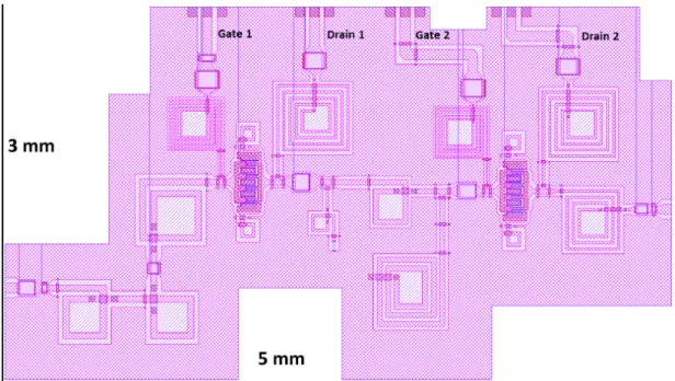
In order to fabricate the whole design, HEMTs are added to layout. Dimension of two stage LNA is 2 mm to 3.5 mm.
Layout of the second LNA design is shown in Figure 4.22. Photograph of the fabricated second LNA design is shown in Figure 4.23. RFin and RFout probes have three legs (ground-signal-ground) and DC supply probes have two legs (supply and ground).
Figure 4.23: Photograph of the second LNA design
4.3.4
Simulation Results
In simulation of this design, we achieved higher than 21 dB gain (21.7 dB to 24.2 dB), more than 12 dB input return loss (12 dB to 13.2 dB), more than 17 dB output return loss (17.1 dB to 21.3 dB) and less than 1.3 dB noise figure (1.1 dB to 1.3 dB) in S band. Simulation results are shown in Figure 4.24a, Figure 4.24b, and Figure 4.24c. Less than 1.5 dB NF is achieved within 1.6 GHz-4.8 GHz band which is better than the requirements (less than 2 dB NF within 2.7 GHz-3.5 GHz band). This result shows that the design satisfies the requirement more than enough.
(a) (b)
(c)
Figure 4.24: a) |S11| and |S22| simulation results of the second LNA design, b)
|S21| simulation curves of the second LNA design, c) NF simulation curve of the
4.3.5
Effect of SiN Thickness Variance
In the first design effect of SiN thickness variance is observed. In the second design this problem is overcomed by reducing the of number capacitors. In the second design only necessary capacitors are included, which are bypass and DC block capacitors. Capacitor values are increased so that the variances in their values can be tolerated in the RF characteristics. SiN thickness variance simulation of the second LNA design is shown in Figure 4.25.
Figure 4.25: SiN thickness variance simulation of the second LNA design
SiN thickness variance simulation results of the second LNA design is shown in Figure 4.26. Changes in the values of NF, S21, S11, S22 are 0.02 dB, 0.3 dB,
Figure 4.26: SiN thickness variance simulation results of the second LNA design
4.4
Third LNA Design
There are two major differences between the second LNA design and the third LNA design; mesa resistor is used at gate biasing circuitries and Lg is changed
from 0.25 µm to 0.15 µm in the third LNA design. Input, output and interstage matching circuitries are the same with the second LNA design. Same procedure is followed for stability check and no change is observed.
As it is mentioned in Chapter 3, mesa sheet resistance varies between 400 to 500 Ohm/square. In the gate biasing 4 kΩ to 5 kΩ mesa resistor is used. Actually the exact value of this resistor is not so critical since it is not used for matching purposes. This mesa resistor does not affect the efficiency of the LNA because gate current flow is only few µA. In the literature, there are analysis for the effects of this mesa resistor to survivability of the LNA [22, 23]. Simplified schematic of the third LNA design is shown in Figure 4.27.
Figure 4.27: Simplified schematic of the third LNA design
Layout of the third LNA design is shown in Figure 4.28.
Chapter 5
Measurement Setups and Results
5.1
Measurement Setups
5.1.1
S-Parameter and Group Delay Measurement Setup
In the s-parameter and group delay measurements Rohde Schwarz ZVA40 Vec-tor Network Analyzer, VNA, and Power Network Analyzer-X, PNA-X, are used. Thru-Open-Short-Match (TOSM) on-wafer calibration is done before measure-ments. Input power level is set to -20 dBm to ensure that the measurements are done in linear region. S-parameter and group delay measurements have the same calibration procedure except changing the measurement type at the VNA. S-parameter and group delay measurement setup is shown in Figure 5.1.
Figure 5.1: S-parameter and group delay measurement setup
5.1.2
Noise Figure Measurement Setup
In noise figure measurements we used Maury’s noise switch and receiver modules, noise source, source tuner, DC power supplies, on-wafer measurment setup and PNA-X. ATS software is used to perform the noise system calibration, verification and measurement. At first source tuner, noise receiver module, noise switching module and PNA-X are added to ATS software configuration. In the noise fig-ure calibration procedfig-ure there are two separate calibrations. First calibration is done to characterize the tuner and also to measure the necessary s-parameters for the system. Second calibration is done for the noise receiver. First, we verified the input network s parameters and then excess noise ratio, ENR, table of the noise source is entered. It has two reflection coefficients of the noise source, when noise source is on (hot) state and when noise source is off (cold) state. Then we measured the noise load reflection coefficient. We chose fixed position for the tuner, then we made the tuner characterization after that in-situ calibration is done. Then we calibrated the noise receiver. After noise receiver calibration we can measure the noise of the DUT. PNA-X gives the Fmin, Γopt, rn and S21.
This noise figure measurement procedure is named as “ultra-fast noise measure-ment method” by Keysight [24]. NF measuremeasure-ment setup is shown in Figure 5.2. Photography of the NF measurement setup is depicted in Figure 5.3
Figure 5.2: NF measurement setup
5.1.3
1 dB Compression Point Measurement Setup
In the 1 dB compression point measurement two DC supplies (to give DC bias the amplifier), one signal generator (to give RF input signal to the amplifier), one on wafer measurement setup, and one spectrum analyzer (to measure output power level) are used. Correctness of the output power is also checked via power meter. Before doing the measurement, cable and on wafer probe losses are measured and noted. Data of these losses are used in the calculation of the P1dB measurement. P1dB measurement setup is shown in Figure 5.4. Input signal is given at 3 GHz and power level is started from -20 dBm and is increased with 1 dB steps.
5.1.4
Third Order Intercept Point Measurement Setup
In the third order intercept point (TOI) measurement two DC supplies (to give DC bias the amplifier), two signal generators (to give RF input signal to the am-plifier), one combiner (to combine two fundamental signals), one on wafer mea-surement setup, and one spectrum analyzer (to measure output power) are used. Correctness of the output power is also checked via power meter. Before doing the measurement, cable, combiner and on wafer probe losses are measured and noted. Data of these losses are used in the calculation of the TOI measurement. TOI measurement setup 1 is shown in Figure 5.5. Spectrum analyzer calculates TOI, however it can be calculated according to formula 5.1. Input signal level is started from -15 dBm and is increased with 1 dB steps [25]. Abbreviations explanations and frequency values are given as;
F is the fundamental signal level (dBm) (Lower Base f1 = 2.999 GHz and
Upper Base f2 = 3.001 GHz)
IMD is the difference between F and 3rd order intermodulation distortion signal level (dBc) (3rd Order Lower 2f1-f2 = 2.997 GHz and 3rd Order
Upper 2f2-f1 = 3.003 GHz)
TOI stands for third order intercept point (dBm) TOI = F + IM D
Figure 5.5: Third order intercept point measurement setup 1
In order to check the correctness of my results, the second setup is constructed. It contains two DC supplies (to give DC bias the amplifier), one combiner (to combine two fundamental signals), one on wafer measurement setup, and ZVA40 VNA. ZVA40 has 4 ports which enables to generate signals from port 1 and port 3. Port 2 is used to measure fundamental and third order products. TOI measurement setup 2 is shown in Figure 5.6
Figure 5.6: Third order intercept point measurement setup 2
5.2
Measurement Results
5.2.1
Measurement Results of the First LNA Design
NF and S-parameter: In this design, we achieved higher than 23.9 dB gain (23.9 dB to 26.5 dB), better than 9.2 dB input return loss (9.2 dB to 16.8 dB), better than 10.1 dB output return loss (10.1 dB to 14.1 dB) and less than 2.5 dB noise figure (1.7 dB to 2.5 dB) in S band. Measurement results of the First LNA Design are shown in Figure 5.7. Simulation and measurement results show a close correlation as can be seen at simulation and measurement comparison section.
Figure 5.7: NF and S-parameter measurements of the first LNA
TOI: Linearity was not a top priority requirement, therefore we did not do any simulation for harmonic products. Simulation time, which is spent during the design, is concentrated on NF and s-parameter simulations. TOI measurement results are close to satisfy the requirements at the first design (the second and third designs satisfy the requirement). TOI measurement of the First LNA Design is shown in 5.8. Measured TOI value is 28.1 dBm at the worst case.
Figure 5.8: TOI measurement result of the first LNA design via spectrum analyzer
Using harmonic measurement setup 2, is shown in Figure 5.6, the following results (shown in Figure 5.9)are obtained. TOI measurement that is taken from ZVA can be seen at right trace (shown in red box). Spectrum analyzer measure-ment is 28.1 dBm and ZVA40 measuremeasure-ment is 28.2 dBm. Group delay is 292 pico seconds.
Figure 5.9: TOI measurement result of the first LNA design via ZVA40 VNA
Output Power at 1 dB Compression: Using P1dB measurement setup, 1 dB compression point is measured. Input signal is given at 3 GHz and power level is started from -20 dBm and is increased with 1 dB steps. Difference between out-put and inout-put powers gives the gain of the DUT. Therefore, gain is noted during the input power sweep. Input power is increased till 1 dB compression. Gain is compressed after -7.8 dBm input power, which justifies harmonic measurements again. Reminder Input power (-7.8 dBm) at 1dB compression point plus gain (25 dB) gives the output power (18.2 dBm) at 1 dB compression(P1dB). In theory P1dB point is 10 dB less than TOI. With this measurement we understand the linear range of the amplifier. In Figure 5.10a input power vs gain of the first LNA design is shown. In Figure 5.10b input power vs output power is depicted.
(a) (b)
Figure 5.10: a) Input Power vs Gain, b) Input Power vs Output Power
5.2.2
Measurement Results of the Second LNA Design
NF and S-parameter: In this design, we achieved higher than 20.4 dB gain (20.4 dB to 21 dB), better than 9.5 dB input return loss (9.5 dB to 11.3 dB), better than 17.3 dB output return loss (17.3 dB to 28.6 dB) and less than 1.68 dB noise figure (1.3 dB to 1.68 dB) in S band. Measurement results of the Second LNA Design are shown in Figure 5.11. Simulation and measurement results show a close correlation.
Figure 5.11: NF and S-parameter measurements of the second LNA
Group Delay: Group delay is the derivative of the DUT’s phase with respect to frequency. It shows the phase distortion that makes the DUT. Group delay measurement result of the Second LNA Design is shown in Figure 5.12. It is only 264 pico second. When we consider the frequency, it is almost distortionless technology. Device can be used in time domain applications.
Figure 5.12: Group delay measurement result of the second LNA design
P1dB and TOI: P1dB measurement result is 23.4 dBm. Achieved TOI value is 33.4 dBm as it is shown in Figure 5.13
Figure 5.13: TOI measurement result of the second LNA design via spectrum analyzer
5.2.3
Measurement Results of the Third LNA Design
NF and S-parameter: In this design, we achieved higher than 22.1 dB gain (22.1 dB to 25 dB), better than 10.2 dB input return loss (10.2 dB to 10.5 dB), better than 7.9 dB output return loss (7.9 dB to 10.2 dB) and less than 1.1 dB noise figure (0.9 dB to 1.1 dB) in S band. Measurement results of the Third LNA Design are shown in Figure 5.14.
Figure 5.14: NF and S-parameter measurements of the third LNA
Highest TOI achieved at this design, is 35.9 dBm. P1dB is 25.9 dBm. Group delay is 269 pico seconds.
Figure 5.15: TOI measurement result of the third LNA design via spectrum analyzer
To have a better understanding on OIP3 measument input power vs output power of the fundamental and third order product signal levels are given at Fig-ure 5.16.
Figure 5.16: 3rd order and fundamental signal levels vs input power measurement result of the third LNA design
5.3
Simulation and Measurement Comparison
Simulation and measurement comparison of the LNA designs are listed in Table 5.1. Simulation and measurement results show close correlation, at 3rd LNA
sub-dB noise figure is achieved. All three LNA designs achieve higher than 20 sub-dB gain, 3rdLNA has the highest linearity. Throughout this thesis study, simulations are improved and at 3rd design best measurment results are achieved.
Table 5.1: Simulation and Measurement Comparison of the LNA Designs
Spec. 1
st LNA 2nd LNA 3rd LNA
Simu Meas Simu Meas Simu Meas NF (dB) 1.9 1.7 1.1 1.3 1.1 0.9 |S21| (dB) 24.4 26.5 24.2 21 24.2 25 |S11| (dB) 17.1 16.8 13.2 11.3 13.2 10.5 |S22| (dB) 17.8 14.1 21.3 28.6 21.3 10.2 τg (ns) NA 0.29 NA 0.26 NA 0.27 P1dB (dBm) NA 18.2 NA 23.3 NA 25.9 OIP3 (dBm) NA 28.1 NA 33.4 NA 35.8
In Table 5.2 RF measurement results are compared with the literature. It can be seen that we have approached the results that are obtained in the literature and even we have passed some of them. We have better input insertion loss, higher gain, higher linearity and lower NF.
Table 5.2: Comparison with Literature
Lg (µm) NF (dB) Gain (dB) RLin (dB) OIP3 (dBm) Ref
0.4 2.7 22 4 26 [26] 0.15 1.3 16 8 32 [27] 0.2 4.6 13 13 28.5 [28] 0.35 2.9 17.2 10 19.2 [29] 0.25 1.2 10.3 7 26 [30] 0.4 1.7 26.5 16.8 28.1 1st LNA 0.25 1.3 21 11.3 33.4 2nd LNA 0.15 0.9 25 10.5 35.8 3rd LNA
Chapter 6
Conclusion and Future Work
In this thesis study design, fabrication and test of three GaN HEMT based MMIC LNAs are presented. Sub-dB NF measurement value is achieved. High gain, low NF and high linearity design approaches are studied. High gain values are achieved. Unconditional stability is an important parameter for amplifier designs, none of LNA designs were oscillated in this thesis study.
Inductive source feedback topology is used to obtain both better input return loss and noise figure. All three designs achieve higher than 20 dB gain, better than 10 dB input return loss and their noise figure values are 2 dB, 1.5 dB and 1 dB in S-band. Size reduction is very important in MMIC technology. The first design is 3 x 5 mm and the second design is 2 x 3.5 mm, % 46 size reduction is achieved. In GaN technology controlling SiN layer thickness is very problematic and this fabrication step affects capacitor values. The second and third LNA designs presented in this research, matching circuitries and implicitly overall characteristics are not influenced too much by a change of capacitor values. Targeted bandwidth is 2.7-3.5 GHz, achieved frequency range is 1.5 GHz (from 2.5 GHz to 4 GHz). The three LNA designs have 28.1 dBm, 33.4 dBm, and 35.9 dBm output third-order intercept point respectively. Output powers at 1-dB compression points are 18.2 dBm, 23.4 dBm and 25.9 dBm. For all three LNA designs, group delay is less than 0.3 nanoseconds.
For the future work, cascode topology can be studied for the broadband LNA design [31]. Robustness will be studied to increase input power handling capa-bility. OIP3 can be studied and improved to have better understanding of the linearity [32]. Novel design approachs can be studied, for instance dual band de-signs can be investigated [27]. In next generation LNA dede-signs, especially for the 5G applications, multi band applications will be favored over usual LNA designs.